 | –≠–ª–µ–∫—Ç—Ä–æ–Ω–Ω—ã–π –∫–æ–º–ø–æ–Ω–µ–Ω—Ç: FHX13X | –°–∫–∞—á–∞—Ç—å:  PDF PDF  ZIP ZIP |
Item
Saturated Drain Current
Transconductance
Pinch-off Voltage
Gate Source Breakdown Voltage
Noise Figure
Associated Gain
Noise Figure
Associated Gain
Symbol
IDSS
10
30
60
35
50
-
-0.1
-
-0.7
-1.5
0.45
0.50
-3.0
-
-
11.0
13.0
-
11.0
13.0
-
-
0.55
0.60
VDS = 2V, IDS = 1mA
VDS = 2V, IDS = 10mA
VDS = 2V, VGS = 0V
IGS = -10µA
VDS = 2V
IDS = 10mA
f = 12GHz
mA
mS
V
dB
dB
dB
dB
V
gm
FHX13X
FHX14X
Vp
VGSO
NF
Gas
NF
Gas
Test Conditions
Unit
Limit
Typ.
Max.
Min.
ELECTRICAL CHARACTERISTICS (Ambient Temperature Ta=25
∞C)
Note: RF parameter sample size 10pcs. criteria (accept/reject)=(2/3)
Channel to Case
-
220
300
∞C/W
Thermal Resistance
Rth
The chip must be enclosed in a hermetically sealed environment for optimum performance and reliability.
1
Edition 1.2
July 1999
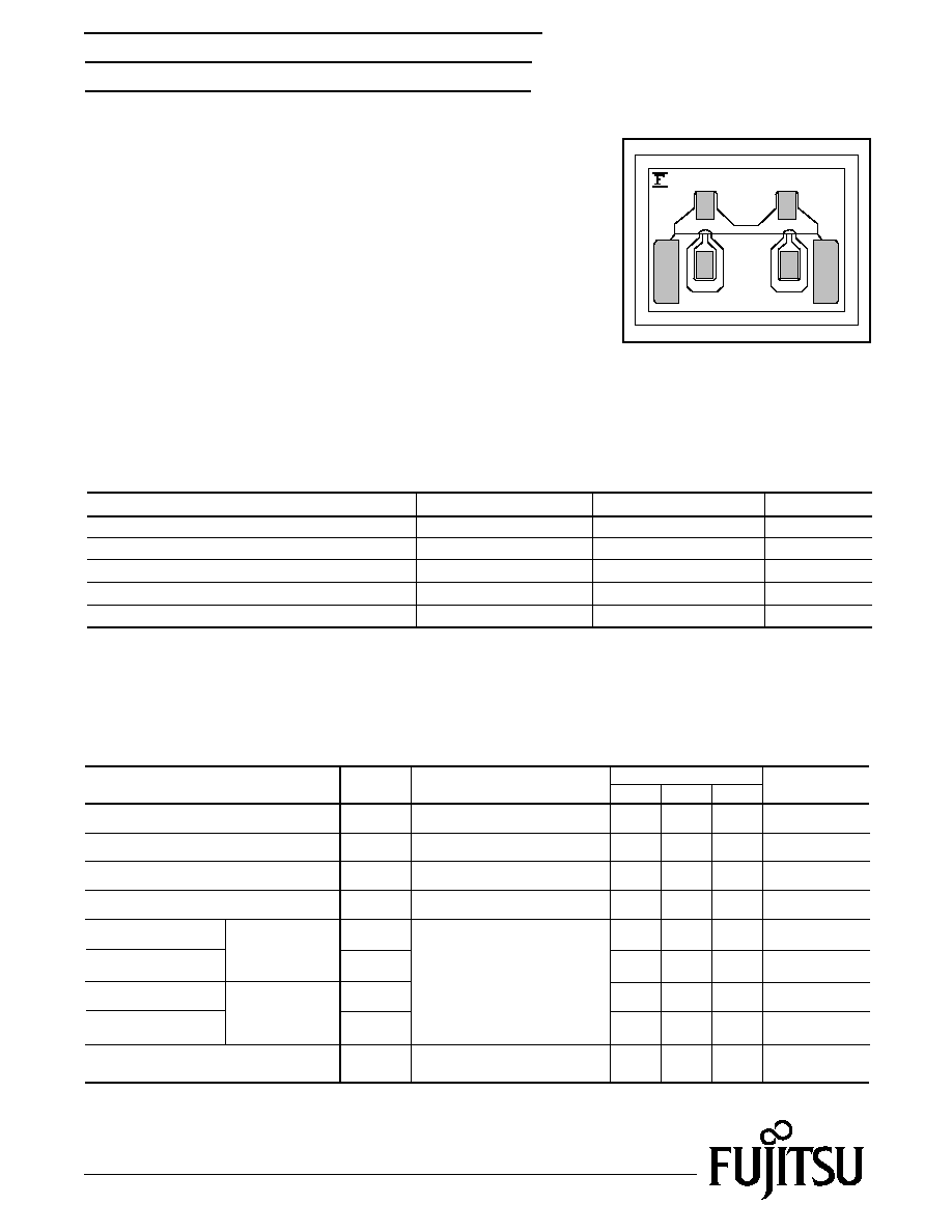
FHX13X, FHX14X
GaAs FET & HEMT Chips
Item
Drain-Source Voltage
Gate-Source Voltage
Total Power Dissipation
Storage Temperature
Channel Temperature
Symbol
VDS
VGS
3.5
-3.0
180
-65 to +175
175
V
V
mW
∞C
∞C
Pt*
Tstg
Tch
Unit
Rating
ABSOLUTE MAXIMUM RATING (Ambient Temperature Ta=25
∞C)
*Note: Mounted on Al2O3 board (30 x 30 x 0.65mm)
Fujitsu recommends the following conditions for the reliable operation of GaAs FETs:
1. The drain-source operating voltage (VDS) should not exceed 2 volts.
2. The forward and reverse gate currents should not exceed 0.2 and -0.05mA respectively with
gate resistance of 4000
.
3. The operating channel temperature (Tch) should not exceed 80∞C.
FEATURES
∑ Low Noise Figure: 0.45dB (Typ.)@f=12GHz (FHX13)
∑ High Associated Gain: 13.0dB (Typ.)@f=12GHz
∑ Lg
0.15µm, Wg = 200µm
∑ Gold Gate Metallization for High Reliability
DESCRIPTION
The FHX13X, FHX14X are Super High Electron Mobility Transistor
(SuperHEMT
TM
) intended for general purpose, ultra-low noise and
high gain amplifiers in the 2-18GHz frequency range. The devices
are well suited for telecommunication, DBS, TVRO, VSAT or other
low noise applications.
Fujitsu's stringent Quality Assurance Program assures the highest
reliability and consistent performance.

2
FHX13X, FHX14X
GaAs FET & HEMT Chips
NF & Gas vs. IDS
DRAIN CURRENT vs. DRAIN-SOURCE VOLTAGE
OUTPUT POWER vs. INPUT POWER
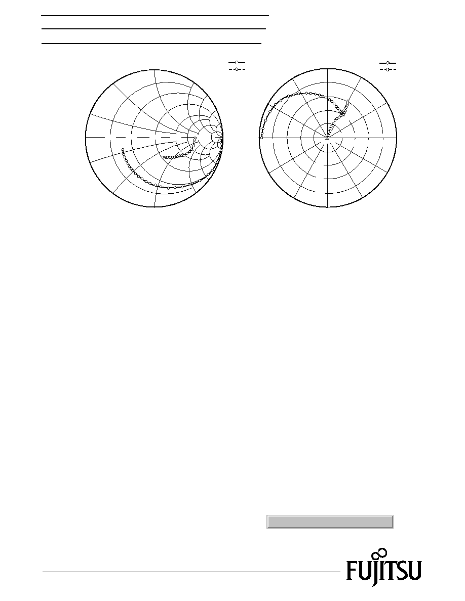
NOISE PARAMETERS
VDS=2V, IDS=10mA
3.0
f=12GHz
VDS=2V
Freq.
(GHz)
opt
(MAG) (ANG)
NFmin
(dB)
Rn/50
f=12GHz
VDS=2V
IDS=10mA
Gas
NF
2.5
2.0
1.5
1.0
0.5
14
13
12
11
10
9
10
20
30
-10
10
-5
0
5
1
2
3
4
Drain Current (mA)
Input Power (dBm)
Drain-Source Voltage (V)
Noise Figure (dB)
40
30
20
0
10
10
15
20
5
0
Drain Current (mA)
Output Power (dBm)
Associated Gain (dB)
2
4
6
8
10
12
14
16
18
20
22
24
0.92
0.84
0.77
0.71
0.66
0.61
0.58
0.56
0.54
0.52
0.50
0.46
13
25
38
51
65
79
93
108
122
136
150
162
0.28
0.30
0.32
0.34
0.39
0.45
0.56
0.68
0.86
1.03
1.22
1.43
0.65
0.54
0.41
0.31
0.23
0.17
0.12
0.09
0.07
0.07
0.07
0.07
VGS =0V
-0.2V
-0.4V
-0.6V
-0.8V
POWER DERATING CURVE
50
100
150
200
Ambient Temperature (
∞C)
200
150
100
0
0
50
Total Power Dissipation (W)
Ga (max) & |S21|2 vs. FREQUENCY
VDS=2V
IDS=10mA
Ga (max)
|S21|2
15
20
25
10
5
0
4
6
8 1012
20
Frequency (GHz)
Gain (dB)
3
FHX13X, FHX14X
GaAs FET & HEMT Chips
+j250
+j100
+j50
+j25
+j10
0
-j10
-j25
-j50
-j100
-j250
S11
S22
180
∞
+90
∞
0
∞
-90
∞
S21
S12
SCALE FOR |S
21
|
SCALE FOR |S12|
.20
.05
.10
.15
2
1
3
4
1
1 GHZ
1 GHZ
1 GHZ
1 GHZ
12
12
12
12
24
24
24
24
5
100
10
25
50
S-PARAMETERS
VDS = 2V, IDS = 10mA
FREQUENCY
S11
S21
S12
S22
(MHZ)
MAG
ANG
MAG
ANG
MAG
ANG
MAG
ANG
100
1.000
-0.9
4.899
179.2
0.001
89.5
0.601
-0.5
500
0.999
-4.7
4.894
175.9
0.006
87.7
0.601
-2.3
1000
0.995
-9.4
4.876
171.9
0.013
85.5
0.599
-4.6
2000
0.981
-18.6
4.806
163.9
0.025
81.1
0.591
-9.2
3000
0.958
-27.7
4.696
156.1
0.037
77.0
0.580
-13.5
4000
0.929
-36.4
4.555
148.6
0.048
73.2
0.565
-17.7
5000
0.895
-44.9
4.392
141.5
0.057
69.8
0.548
-21.5
6000
0.860
-53.0
4.215
134.8
0.066
66.8
0.530
-25.0
7000
0.823
-60.7
4.034
128.4
0.074
64.2
0.512
-28.3
8000
0.786
-68.1
3.852
122.4
0.080
62.0
0.493
-31.3
9000
0.751
-75.3
3.675
116.8
0.086
60.2
0.475
-34.0
10000
0.718
-82.1
3.506
111.5
0.092
58.9
0.458
-36.6
11000
0.687
-88.7
3.345
106.5
0.096
57.8
0.442
-39.0
12000
0.659
-95.0
3.194
101.8
0.101
57.1
0.426
-41.3
13000
0.633
-101.2
3.054
97.3
0.105
56.6
0.412
-43.6
14000
0.610
-107.2
2.923
93.0
0.108
56.4
0.399
-45.8
15000
0.590
-113.0
2.801
88.9
0.112
56.4
0.386
-47.9
16000
0.572
-118.7
2.688
85.0
0.116
56.6
0.375
-50.1
17000
0.556
-124.2
2.584
81.3
0.120
56.9
0.364
-52.3
18000
0.543
-129.6
2.487
77.7
0.124
57.3
0.353
-54.6
19000
0.532
-134.9
2.397
74.2
0.129
57.8
0.344
-56.9
20000
0.523
-140.0
2.314
70.8
0.133
58.4
0.335
-59.4
21000
0.516
-145.0
2.236
67.5
0.138
58.9
0.326
-62.0
22000
0.511
-149.8
2.164
64.4
0.144
59.5
0.318
-64.7
23000
0.507
-154.6
2.096
61.3
0.150
60.0
0.310
-67.5
24000
0.505
-159.2
2.033
58.3
0.156
60.5
0.303
-70.5
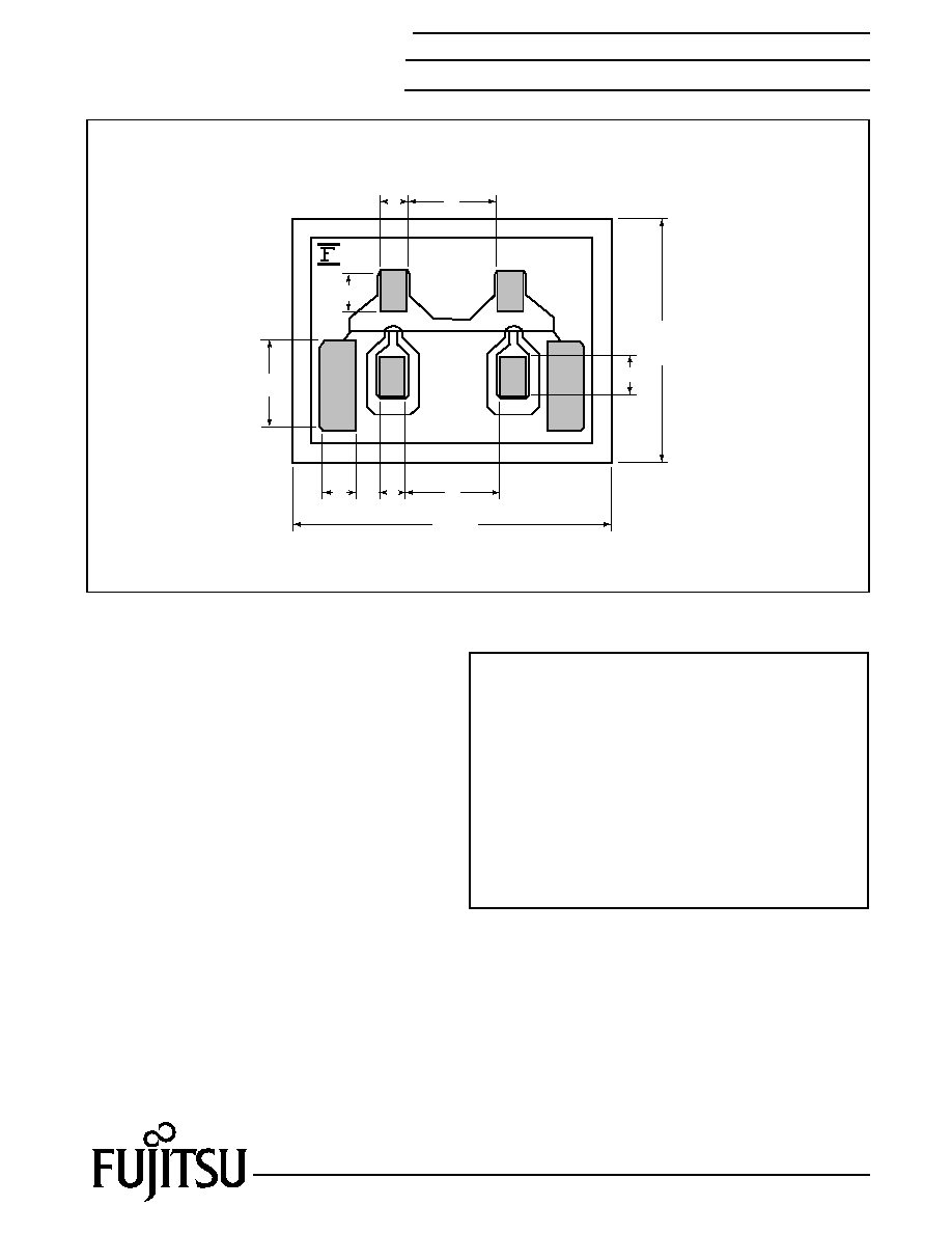
NOTE:*
The data includes bonding wires.
n: number of wires
Gate
n=2 (0.3mm length, 20µm Dia Au wire)
Drain n=2 (0.3mm length, 20µm Dia Au wire)
Source n=4 (0.3mm length, 20µm Dia Au wire)
Download S-Parameters, click here
For further information please contact:
FUJITSU COMPOUND SEMICONDUCTOR, INC.
2355 Zanker Rd.
San Jose, CA 95131-1138, U.S.A.
Phone: (408) 232-9500
FAX: (408) 428-9111
www.fcsi.fujitsu.com
FUJITSU MICROELECTRONICS, LTD.
Compound Semiconductor Division
Network House
Norreys Drive
Maidenhead, Berkshire SL6 4FJ
Phone:+44 (0)1628 504800
FAX:+44 (0)1628 504888
Fujitsu Limited reserves the right to change products and specifications without notice.
The information does not convey any license under rights of Fujitsu Limited or others.
© 1998 FUJITSU COMPOUND SEMICONDUCTOR, INC.
Printed in U.S.A. FCSI0598M200
Fujitsu Compound Semiconductor Products contain gallium arsenide
(GaAs) which can be hazardous to the human body and the environment.
For safety, observe the following procedures:
CAUTION
∑ Do not put these products into the mouth.
∑ Do not alter the form of this product into a gas, powder, or liquid
through burning, crushing, or chemical processing as these by-products
are dangerous to the human body if inhaled, ingested, or swallowed.
∑ Observe government laws and company regulations when discarding this
product. This product must be discarded in accordance with methods
specified by applicable hazardous waste procedures.
4
CHIP OUTLINE
(Unit:
µm)
96
60
96
450
±20
154
350
±
20
60
70
44
44
Die Thickness:
100
±20µm
FHX13X, FHX14X
GaAs FET & HEMT Chips
SuperHEMT
TM
is a trademark of Fujitsu Limited.