 | –≠–Ľ–Ķ–ļ—ā—Ä–ĺ–Ĺ–Ĺ—č–Ļ –ļ–ĺ–ľ–Ņ–ĺ–Ĺ–Ķ–Ĺ—ā: FID3S1KX | –°–ļ–į—á–į—ā—Ć:  PDF PDF  ZIP ZIP |
FEATURES
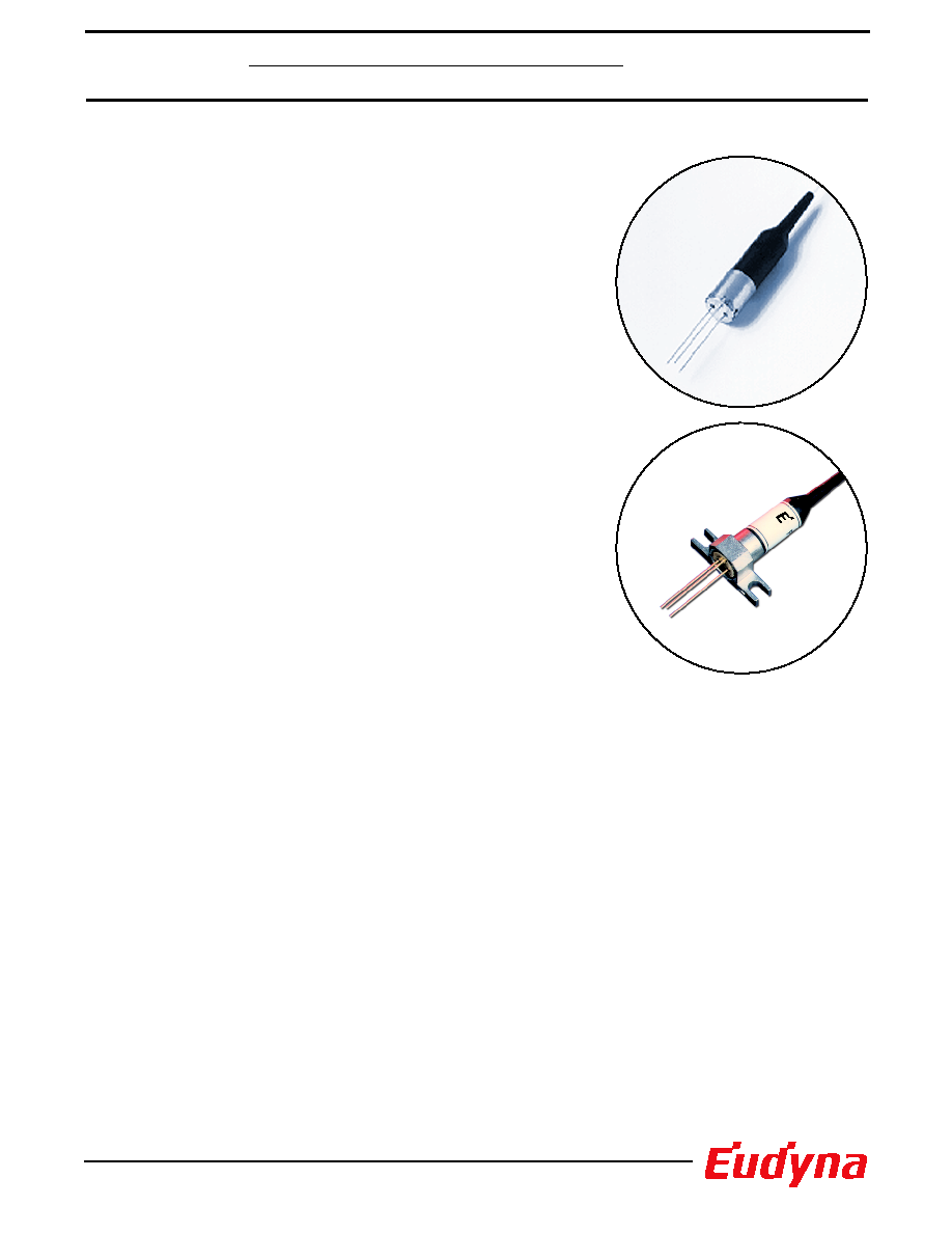
∑ Hermetically Sealed Package with a single mode
fiber pigtail
∑ High Responsivity: 0.85 A/W
∑ Low Dark Current: 0.1 nA
∑ Low Distortion: < -75dBc
∑ High Optical Return Loss: > 40dB
∑ High Frequency Response: 2.0GHz
APPLICATIONS
∑ Analog Transmission Systems
∑ AM and FM CATV systems
DESCRIPTION
The FID3S1HX/KX are PIN photodiode modules with a single mode
fiber pigtail specifically designed for multichannel analog transmission
systems. The photodiode uses a planar structure to achieve
low dark current, high responsivity and high reliability. The coupling
optics in the package is designed for very low optical reflection.
The package is hermetically sealed.
Edition 1.2
July 2004
1
FID3S1HX/KX
HX
KX
Analog PIN
Photodiode
2
FID3S1HX/KX
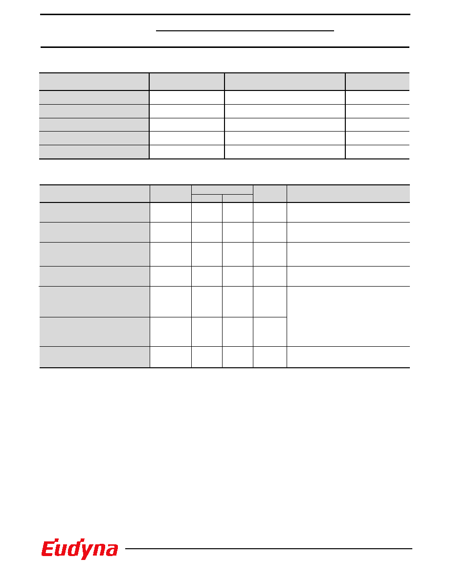
Parameter
Responsivity
Cut-off Frequency
Capacitance
2nd order intermodulation
distortion
3rd order intermodulation
distortion
Symbol
R
fc
Ct
IMD2
IMD3
(1) Modulation input light signals are from two independent laser sources with a modulation frequency f1=244 MHz and f2=250 MHz
f=1MHz, VR=5V
RL=50, VR=5V,
-3dB from 500KHz
VR=1V
VR=5V
2 laser, 2 tone, OMD=70% each,
Pin=-0dBm,
VR=5V (Note 1)
Conditions
OPTICAL & ELECTRICAL CHARACTERISTICS (Ta=25įC, =1300 and 1500nm)
A/W
GHz
pF
dBc
dBc
Unit
Limits
-
-
1.3
Max.
0.8
Dark Current
ID
nA
5
-
1.5
-75
-
-90
-
-
Optical return loss
ORL
dB
-
40
Min.
Parameter
Storage Temperature
Operating Case Temperature
Forward Current
Reverse Current
Reverse Voltage
Symbol
Tstg
-40 to +85
-40 to +80
5
3
20
mA
mA
V
įC
įC
Top
IF
IR
VR
Ratings
Unit
ABSOLUTE MAXIMUM RATINGS (Ta=25įC)
respectively.
(2) Pigtail fiber: Singlemode fiber, core diameter 10
Ī1Ķm, cladding diameter 125Ī2Ķm, difference of refractive index 0.3%.
(3) VR = 10V is recommended at Pin > 0dBm or f > 1GHz application.
Analog PIN
Photodiode
3
FID3S1HX/KX
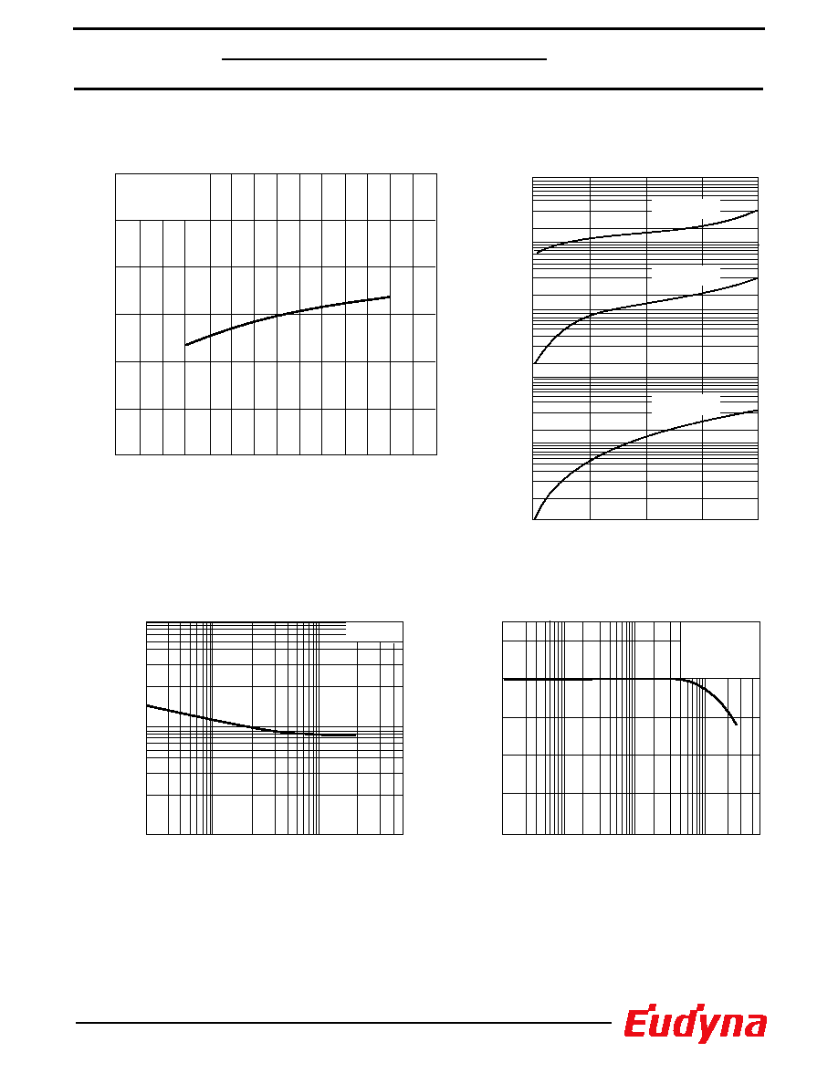
Fig. 1 Temperature Dependence of Responsivity
Temperature, Ta (
įC)
Normalized Responsivity,
R/R (25
į
C) (%)
6
-6
-4
-2
2
4
0
40
60
80
20
0
-20
-40
= 1300nm
VR = 1V
Fig. 2 Dark Current vs. Reverse Voltage
10
5
50
0.5
0.2
1
Reverse Voltage, VR (V)
Ta = 25įC
Fig. 3 Capacitance vs. Reverse Voltage
Fig. 4 Frequency Response
Capacitance, Ct (pF)
Response (dB)
1
0.1
10
-3
-9
-6
0
2
10
102
103
Frequency (MHz)
Ta=25įC
f=1 MHz
VR = 5V
RL = 50
= 1300nm
Dark Current, I
D
(A)
10
20
0
10-12
10-13
10-10
10-9
10-8
10-11
Reverse Voltage, VR (V)
Ta = 25įC
Ta = -40įC
Ta = 85įC
Analog PIN
Photodiode
4
Analog PIN
Photodiode
FID3S1HX/KX
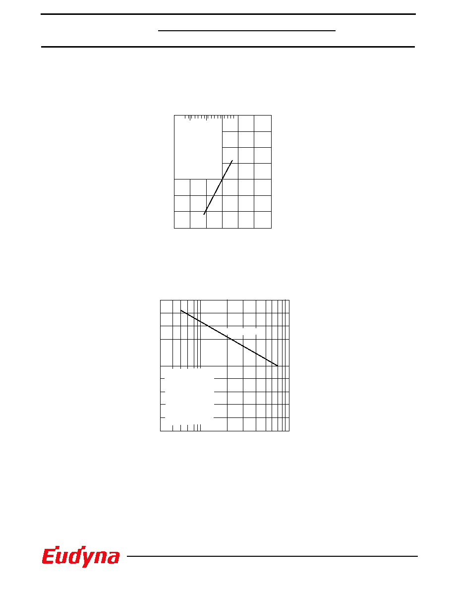
Fig. 5 2nd Order Intermodulation
Distortion Characteristics
2 Tone, 2LD test
Ta=25
įC
=1300 nm
f1=244 MHz
f2=250 MHz
OMD=70% each
RL=50
VR=5V
2 Tone, 2LD test
Ta=25
įC
=1300 nm
f1=244 MHz
f2=250 MHz
RL=25
VR=5V
Fig. 6 Frequency Response
Output Power of Fundamentals, Pout (dBm)
Total Received Optical Power, Pin (dBm)
Optical Modulation Depth/ch, OMD (%)
Output Power of 2nd order
intermodulation products (dBm)
2nd order intermodulation
distortion, IMD2 (dBm)
-60
-40
10
Pin=-0dBm
-20
0
-10
-5
0
+5
-140
-120
-100
-80
-60
-100
-80
100
5
Analog PIN
Photodiode
FID3S1HX/KX
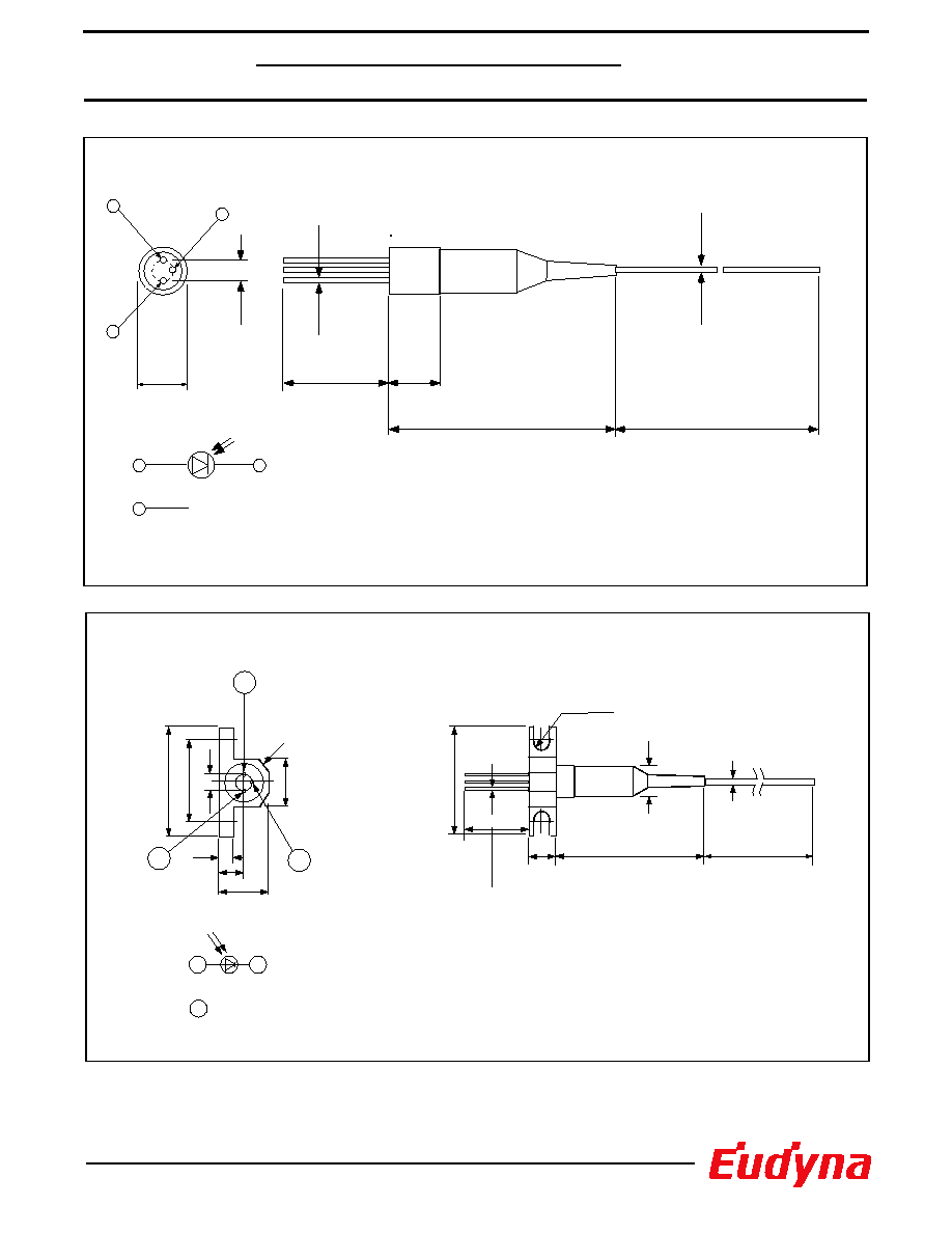
11MIN
1
2
3
CASE
PD
1
3
2
31
Ī1
1000 MIN
Ý
0.9
7.3 MAX
3-
Ý
0.35
Ý
2.54
Ý6
Ī0.1
"HX" PACKAGE
UNIT: mm
1
2
3
ANODE
CATHODE
CASE
4
2 - R 1.25
2 - C1.5
2.0
3.7
7.4
2
3
1
1000 MIN.
28 MAX.
17.0
Ý
2.54
17.0
Ý
6.0 MAX.
Ý
0.9
3-
Ý
0.35
12.7
7.4
10 MIN.
"KX" PACKAGE
UNIT: mm