1
Edition 1.3
July 2004
FLD5F20NP-C
Parameter
Symbol
Storage Temperature
Tstg
+85
-
∞
C
-40
Operating Case Temperature
+70
-
∞
C
Top
-20
Optical Output Power
5
CW
mW
Pf
-
Laser Forward Current
150
CW
mA
IF
-
Laser Reverse Voltage
2
CW
V
VR
-
Modulator Forward Voltage
+1
CW
V
Vm
-5
Photodiode Forward Current
1
-
mA
-
-
10
-
V
Photodiode Reverse Voltage
VDR
-
10
260
∞C
sec
Lead Soldering Time
-
-
TEC Voltage
+2.5
Cooling
-
Heating
V
Vc
-
-2.5
TEC Current
+1.4
Cooling
-
Heating
A
Ic
-
-0.9
Thermistor Temperature
+70
-20
ATC Operation
∞C
Tth
Rating
Unit
Min.
Max.
ABSOLUTE MAXIMUM RATINGS (Top=25∞C, unless otherwise specified)
Condition
1,550nm Modulator
Integrated DFB Laser
FEATURES
∑ Modulator Integrated DFB Laser Diode Module
∑ CW operation of DFB laser section
∑ Modulation voltage applied only to modulator section
∑ High speed butterfly package with GPO connection
∑ Built-in optical isolator, monitor photodiode, thermistor, and
thermo-electric cooler
APPLICATION
This MI DFB laser is intended for long reach applications (
80km)
at 10Gb/s.
DESCRIPTION
The Modulator Integrated DFB Laser (MI DFB Laser) has an electro-absorption modulator
monolithically integrated with a conventional Distributed Feed-Back (DFB) laser. The modulation
voltage is applied to the modulator section while the laser section operates CW allowing extremely low
wavelength chirping. Extinction ratios of more than 10 dB can be achieved with 2.6 Vp-p modulation.
The MI laser is installed in a butterfly type package. The module incorporates a highly stable optical
coupling system. The module includes an optical isolator, monitor photodiode, thermistor and a
thermo-electric cooler.

2
FLD5F20NP-C
1,550nm Modulator
Integrated DFB Laser
Parameter
Symbol
Unit
Limits
Max.
Type
Min.
Test Condition
Note (1)
Peak Wavelength
Wp
nm
1565
-
1530
Forward Voltage
VF
V
-
2.0
1.4
CW, IF=Iop
Optical Isolation
Is
dB
-
25
35
Tc=-20 to +70
∞C
Threshold Current
Ith
mA
-
30
-
CW, Vm=Vo
Threshold Power
Pth
µW
-
75
-
CW, IF=Ith, Vm=Vo
Output Power
Pf
dBm
-1.0
-
-
Note (1)
Tracking Error
TE
dB
-0.5
+0.5
-
CW, IF=Iop, Vm=Vo, Im-APC,
Tc=-20 to 70
∞C
Spectral Width
p
-
0.04
-
nm
-
0.30
-
10Gb/s, NRZ, PRBS=2
23
-1,
IF=Iop, Vm=Vo & (Vo-Vmod),
-3dB, FWHM
10Gb/s, NRZ, PRBS=2
23
-1,
IF=Iop, Vm=Vo & (Vo-Vmod),
-20dB, FWHM
On Level Modulation
Vo
V
-0.7
0
-
-
Modulator Drive Voltage
Vmod
Vpp
-
2.6
-
(Vo-Vmod)-3.3V,
Rext=10dB
Relative Intensity Noise
RIN
dB/Hz
-
-120
-
f=10MHz to 8.5GHz,
Vm=Vo, IF=Iop, 8% Reflection
Operating Current
Iop
mA
40
100
-
-
Sidemode Suppression Ratio
SSR
dB
-
35
-
Note (1)
Kink
K
-
No Kink
Ith +5mA to 1.5 x Iop
Mode Hops
-
-
No Mode Hops
Ith +5mA to 1.5 x Iop
OPTICAL & ELECTRICAL CHARACTERISTICS (TL= 25∞C, Top = 25∞C, & BOL, unless otherwise specified)

3
FLD5F20NP-C
1,550nm Modulator
Integrated DFB Laser
Parameter
Symbol
OPTICAL & ELECTRICAL CHARACTERISTICS (TL= 25∞C, Top = 25∞C, & BOL, unless otherwise specified)
Note (1) Eudyna Test System, 9.95328Gb/s, PRBS=2
23
-1, IF=Iop, Vm=Vo and (Vo-Vmod)
Note (2) Eudyna Test System, 9.95328Gb/s, PRBS=2
23
-1, IF=Iop, Vm=Vo and (Vo-Vmod)
Dispersion=1600ps/nm, Dispersion Penalty at Bit-Error-Rate=1.0E-10
Unit
Limits
Max.
Type
Min.
Test Condition
Cut-off Frequency
S21
GHz
10
-
-
-3dB, IF=Iop,Vm=Vo-0.5|Vmod|
TEC Power Dissipation
PTEC
W
2.4
-
-
IF=Iop
TEC Capacity
T
∞C
-
45
-
PTEC=2.4W, IF=Iop
TEC Current
ITEC
A
1.0
-
-
IF=Iop, T=45∞C
TEC Voltage
VTEC
V
2.4
-
-
IF=Iop, T=45∞C
TL=25
∞C
Thermal Resistance
Rth
k
10.5
9.5
-
Thermistor B Constant
B
K
3630
3270
3450
In-Band Ripple
G
dB
-1.0
+1.0
-
IF=Iop, 0.1 to 10GHz,
Vm=Vo-0.5|Vmod|
RF Return Loss
S11
dB
8
-
-
dB
5
-
-
DC to 5GHz, Vm=Vo, IF=Iop,
50
Test Set
5 to 10GHz, Vm=Vo, IF=Iop,
50
Test Set
Monitor Current
Im
mA
0.04
1.5
-
Note (1), VDR=5V
Monitor Dark Current
Id
nA
-
100
2
VDR=5V
Monitor Diode Capacitance
Ct
pF
-
15
2
VDR=5V, f=10MHz
Transmission Penalty due
to Dispersion
Pd
dB
-
-
2.0
-
Note (2)
RF Extinction Ratio
Rext
dB
-
-
10
IF=Iop, Vm=Vo at On-Level,
Vm=Vo-Vmod at Off-Level
Rise/Fall Time
Tr, Tf
ps
25
-
20
IF=Iop, Vm=Vo, 20% to 80%
4
FLD5F20NP-C
1,550nm Modulator
Integrated DFB Laser
10 Gb/s
PRBS=2
23
-1
IF=Iop
Vm=Vo/(Vo-2)
Vo=-0.5V
TLD=25∞C
Pf
Im
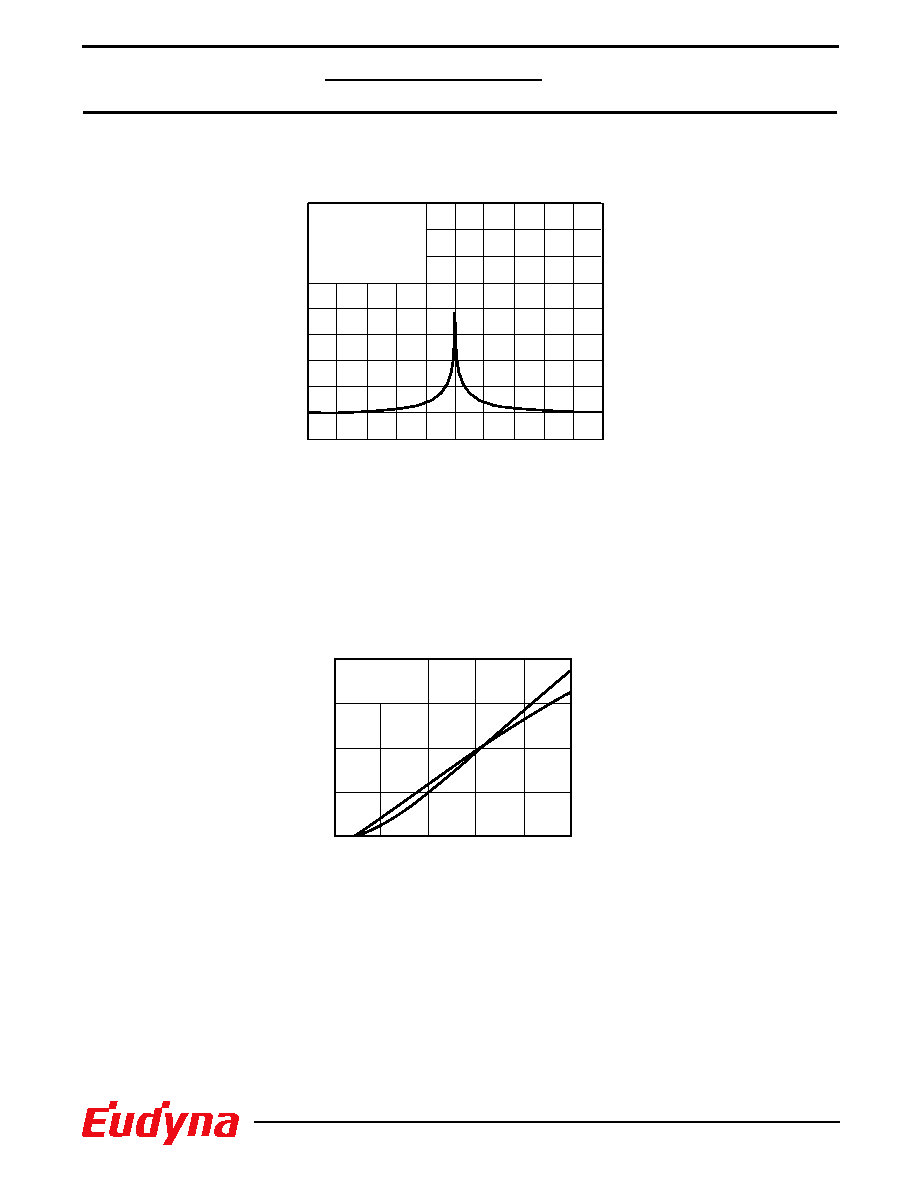
Fig. 1 Lasing Spectrum
Wavelength (Span=1 nm/div, Res.=0.1nm)
Fig. 2 Output Power & Monitor Current
vs. Forward Current
Forward Current, IF (mA)
Output Power, Pf (mW)
Monitor Current, Im (mA)
3
4
2
1
20
40
60
80
100
0
0
0.25
0.5
0.75
1
0
Relative Intensity (10 dB/div.)
5
FLD5F20NP-C
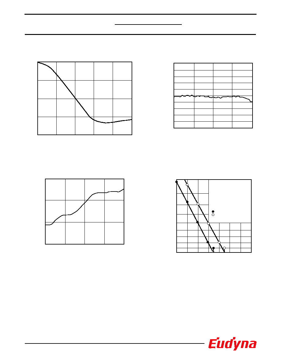
Fig. 3 Extinction Ratio vs.
Modulation Applied Voltage
Fig. 4 Cut-off Frequency (S21)
Frequency, f (GHz)
Modulation Applied Voltage (V)
Extinction Ratio (dB)
Relative Output (dB)
-10
-5
0
-15
-20
0.5
1.0
1.5
2.0
2.5
0
5
10
15
20
0
-12
-9
-6
-3
0
3
6
9
12
Fig. 5 RF Return Loss (S11)
Frequency, f (GHz)
Return Loss (dB)
5
10
15
20
0
-30
-20
-10
0
Fig. 6 Transmission Characteristics
TLD=25
∞C,
ILD=70mA, Vo=-0.5V,
Vpp=2.0V,
9.95328Gb/s,
PRBS=2
23
-1,
Power penalty=+1.0dB
(@BER=10
-10
),
Dispersion=1600 ps/nm
Back to Back
After 1600 ps/nm
Received Optical Power (dBm)
Bit Error Rate
10
-12
10
-10
10
-11
10
-8
10
-9
10
-6
10
-5
10
-7
10
-4
-23
-22
-17
-16
-18
-19
-20
-21
1,550nm Modulator
Integrated DFB Laser