 | –≠–ª–µ–∫—Ç—Ä–æ–Ω–Ω—ã–π –∫–æ–º–ø–æ–Ω–µ–Ω—Ç: FLK207XV | –°–∫–∞—á–∞—Ç—å:  PDF PDF  ZIP ZIP |

1
Edition 1.3
July 1999
FLK207XV
GaAs FET & HEMT Chips
Item
Saturated Drain Current
Transconductance
Pinch-off Voltage
Gate Source Breakdown Voltage
Power-added Efficiency
Output Power at 1dB
Gain Compression Point
Power Gain at 1dB
Gain Compression Point
Symbol
IDSS
-
800
1200
-
400
-
-1.0
-2.0
-3.5
-5
-
-
5
6
-
-
27
-
31.5
32.5
-
VDS = 5V, IDS = 40mA
VDS = 5V, IDS = 500mA
VDS = 5V, VGS = 0V
IGS = -40µA
VDS = 10V
IDS 0.6IDSS
f = 14.5GHz
mA
mS
V
dB
%
dBm
V
gm
Vp
VGSO
P1dB
G1dB
add
Test Conditions
Unit
Limit
Typ.
Max.
Min.
ELECTRICAL CHARACTERISTICS (Ambient Temperature Ta=25∞C)
Note: RF parameter sample size 10pcs. criteria (accept/reject)=(2/3)
Channel to Case
-
10
12
∞C/W
Thermal Resistance
Rth
The chip must be enclosed in a hermetically sealed environment for optimum performance and reliability.
DESCRIPTION
The FLK207XV chip is a power GaAs FET that is
designed for general purpose applications in the
Ku-Band frequency range as it provides superior
power, gain, and efficiency.
Fujitsu's stringent Quality Assurance Program assures the
highest reliability and consistent performance
Gate
Gate
Gate
Drain
Drain
Drain
Drain
Item
Drain-Source Voltage
Gate-Source Voltage
Total Power Dissipation
Storage Temperature
Channel Temperature
Symbol
VDS
VGS
15
-5
12.5
-65 to +175
175
Tc = 25∞C
V
V
W
∞C
∞C
Ptot
Tstg
Tch
Condition
Unit
Rating
ABSOLUTE MAXIMUM RATING (Ambient Temperature Ta=25∞C)
Fujitsu recommends the following conditions for the reliable operation of GaAs FETs:
1. The drain-source operating voltage (VDS) should not exceed 10 volts.
2. The forward and reverse gate currents should not exceed 17.8 and -1.0 mA respectively with
gate resistance of 250.
3. The operating channel temperature (Tch) should not exceed 145∞C.
FEATURES
∑ High Output Power: P1dB = 32.5dBm(Typ.)
∑ High Gain: G1dB = 6.0dB(Typ.)
∑ High PAE: add = 27%(Typ.)
∑ Proven Reliability
2
FLK207XV
GaAs FET & HEMT Chips
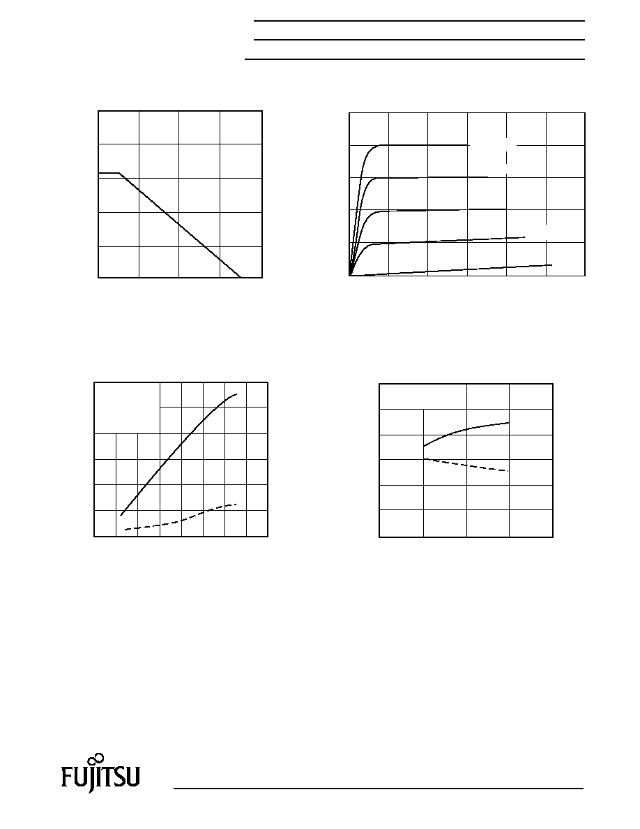
POWER DERATING CURVE
DRAIN CURRENT vs. DRAIN-SOURCE VOLTAGE
8
4
16
12
0
50
100
150
200
2
4
6
8
10
Case Temperature (∞C)
Drain-Source Voltage (V)
Total Power Dissipation (W)
32
30
28
26
24
16
18
20
22
24
26
28
Input Power (dBm)
Output Power (dBm)
1000
Drain Current (mA)
VGS =0V
-0.5V
-1.5V
-2.0V
-1.0V
OUTPUT POWER vs. INPUT POWER
VDS=10V
IDS0.6IDSS
f = 14.5GHz
add
Pout
40
20
add
(%)
32
33
31
30
29
8
9
10
Drain-Source Voltage (V)
P
1dB
(dBm)
P1dB & add vs. VDS
f = 14.5GHz
IDS0.6IDSS
add
P1dB
30
40
20
10
add
(%)
800
600
400
200

3
S-PARAMETERS
VDS = 10V, IDS = 480mA
FREQUENCY
S11
S21
S12
S22
(MHZ)
MAG
ANG
MAG
ANG
MAG
ANG
MAG
ANG
100
.994
-32.9
16.981
162.0
.008
72.9
.177
-152.4
500
.947
-111.8
9.690
118.1
.023
32.8
.361
-153.8
1000
.932
-142.9
5.469
98.1
.026
17.4
.414
-158.5
1500
.929
-155.1
3.712
87.3
.026
11.5
.442
-158.4
2000
.928
-161.6
2.775
79.5
.026
8.5
.469
-157.3
2500
.928
-165.6
2.195
73.0
.025
7.0
.497
-156.1
3000
.929
-168.4
1.799
67.2
.024
6.3
.526
-155.2
3500
.930
-170.6
1.512
61.9
.024
6.4
.556
-154.7
4000
.932
-172.2
1.293
57.1
.023
7.0
.585
-154.5
4500
.933
-173.6
1.122
52.5
.022
8.2
.613
-154.6
5000
.934
-174.7
.984
48.3
.022
9.8
.639
-154.8
5500
.935
-175.8
.870
44.3
.021
12.0
.664
-155.3
6000
.937
-176.7
.776
40.5
.020
14.6
.688
-155.8
6500
.938
-177.5
.696
37.0
.020
17.5
.709
-156.5
7000
.939
-178.3
.628
33.7
.020
20.8
.729
-157.1
7500
.940
-179.0
.569
30.6
.020
24.3
.748
-157.9
8000
.941
-179.6
.518
27.7
.020
27.8
.764
-158.6
8500
.942
179.7
.474
25.0
.020
31.5
.780
-159.4
9000
.943
179.1
.435
22.4
.020
35.0
.794
-160.1
9500
.944
178.5
.400
20.0
.020
38.4
.806
-160.8
10000
.945
178.0
.369
17.8
.021
41.6
.818
-161.5
10500
.945
177.4
.342
15.7
.022
44.6
.829
-162.2
11000
.946
176.9
.317
13.7
.022
47.4
.838
-162.9
11500
.947
176.4
.295
11.9
.023
49.9
.847
-163.6
12000
.947
175.9
.275
10.2
.024
52.2
.856
-164.2
12500
.948
175.4
.257
8.6
.025
54.2
.863
-164.8
13000
.948
174.9
.241
7.2
.026
56.1
.870
-165.4
13500
.949
174.5
.226
5.9
.027
57.7
.876
-166.0
14000
.949
174.0
.212
4.7
.028
59.2
.882
-166.5
14500
.949
173.5
.199
3.6
.029
60.5
.887
-167.1
15000
.950
173.1
.188
2.6
.030
61.6
.892
-167.6
15500
.950
172.7
.177
1.7
.031
62.7
.897
-168.1
16000
.950
172.2
.167
1.0
.033
63.6
.901
-168.6
16500
.951
171.8
.158
0.3
.034
64.4
.905
-169.0
17000
.951
171.4
.149
-0.2
.035
65.1
.909
-169.5
17500
.951
170.9
.141
-0.6
.036
65.8
.912
-169.9
18000
.951
170.5
.134
-0.9
.037
66.3
.915
-170.4
18500
.952
170.1
.127
-1.1
.039
66.9
.918
-170.8
19000
.952
169.7
.121
-1.2
.040
67.3
.921
-171.2
19500
.952
169.3
.115
-1.1
.041
67.7
.923
-171.6
20000
.952
168.9
.109
-1.0
.042
68.0
.925
-171.9
NOTE:*
The data includes bonding wires.
n: number of wires
Gate
n=8 (0.2mm length, 25µm Dia Au wire)
Drain n=8 (0.2mm length, 25µm Dia Au wire)
FLK207XV
GaAs FET & HEMT Chips
Download S-Parameters, click here

For further information please contact:
FUJITSU COMPOUND SEMICONDUCTOR, INC.
2355 Zanker Rd.
San Jose, CA 95131-1138, U.S.A.
Phone: (408) 232-9500
FAX: (408) 428-9111
www.fcsi.fujitsu.com
FUJITSU MICROELECTRONICS, LTD.
Compound Semiconductor Division
Network House
Norreys Drive
Maidenhead, Berkshire SL6 4FJ
Phone:+44 (0)1628 504800
FAX:+44 (0)1628 504888
Fujitsu Limited reserves the right to change products and specifications without notice.
The information does not convey any license under rights of Fujitsu Limited or others.
© 1998 FUJITSU COMPOUND SEMICONDUCTOR, INC.
Printed in U.S.A. FCSI0598M200
Fujitsu Compound Semiconductor Products contain gallium arsenide
(GaAs) which can be hazardous to the human body and the environment.
For safety, observe the following procedures:
CAUTION
∑ Do not put these products into the mouth.
∑ Do not alter the form of this product into a gas, powder, or liquid
through burning, crushing, or chemical processing as these by-products
are dangerous to the human body if inhaled, ingested, or swallowed.
∑ Observe government laws and company regulations when discarding this
product. This product must be discarded in accordance with methods
specified by applicable hazardous waste procedures.
4
Source electrodes are
connected to the PHS
by Via-Hole
Die Thickness: 60±20µm
(Via-Hole)
(Unit: µm)
Gate
Gate
Gate
Drain
Drain
Drain
Drain
1640
60
56
480
70
55
110
58
CHIP OUTLINE
FLK207XV
GaAs FET & HEMT Chips