FEATURES
High Voltage Operation (VDS=28V) GaAs FET
High Gain: 15.5dB(typ.) at Pout=44.8dBm(Avg.)
Broad Frequency Range : 2110 to 2170MHz
High Reliability
DESCRIPTION
The FLL21E135IX is a high power GaAs FET that offers high efficiency,
ease of matching, greater consistency and broad bandwidth for high
power L-band amplifiers. This device is target for high voltage, low
current operation in digitally modulated base station amplifiers. This
product is ideally suited for W-CDMA and Multi-carrier PCS base station
amplifiers while offering high gain, long term reliability and ease of use.
Edition 1.1
June 2004
1
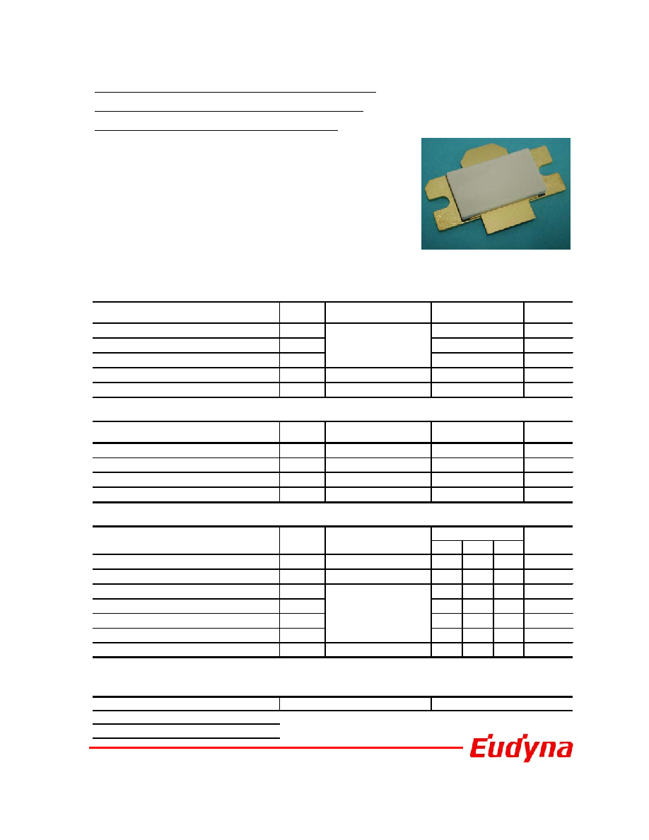
FLL21E135IX
L,S-band High Power GaAs FET
ABSOLUTE MAXIMUM RATING
Item
Symbol
Condition
Unit
Drain-Source Voltage
V
DS
V
Gate-Source Voltage
V
GS
V
Total Power Dissipation
P
T
W
Storage Temperature
T
stg
-
o
C
Channel Temperature
T
ch
-
o
C
RECOMMENDED OPERATING CONDITION (Case Temperature Tc=25
o
C)
Item
Symbol
Condition
Unit
DC Input Voltage
V
DS
V
Forward Gate Current
I
GF
R
G
=2
mA
Reverse Gate Current
I
GR
R
G
=2
mA
Channel Temperature
T
ch
o
C
ELECTRICAL CHARACTERISTICS (Case Temperature Tc=25
o
C)
Min.
Typ. Max.
Pinch-Off Voltage
V
P
V
DS
=5V, I
DS
=226mA
-0.1
-0.2
-0.5
V
Gate-Source Breakdown Boltage
V
GSO
I
GS
=-2.26mA
-5
-
-
V
3rd Order Intermodulation Distortion
IM
3
-
-33
-30
dBc
Power Gain
G
P
14.5
15.5
-
dB
Drain Efficiency
D
-
26
-
%
Adjacent Channel Leakage Power Ratio
ACLR
-
-35
-
dBc
Themal Resistance
R
th
Channel to Case
-
0.8
1.0
o
C/W
Note 1 : IM
3
, ACLR and Gain test conditions as follows
IM
3
& Gain : f
0
=2.1325GHz, f
1
=2.1475GHz W-CDMA(3GPP3.4 12-0) BS-1 64ch non clipping modulation measured over 3.84MHz at f
0
-15MHz and f
1
+15MHz.
ACLR : f
0
=2.1325GHz W-CDMA (3GPP3.4 12-00) BS-1 64ch non clipping modulation, measured over 3.84MHz at f
0
+/-5MHz
ESD
Note : Based on EIAJ ED-4701 C-111A(C=100pF, R=1.5k)
CASE STYLE : IX
CLASS III
2000V ~
T
C
=25
o
C
(Case Temperature)
Rating
32
-3
175
Limit
155
65 to +175
200
<28
<529
>-48
V
DS
=28V
I
DS
(DC)=1000mA
P
out
=44.8dBm(Avg.)
Note 1
Unit
Item
Symbol
Condition
Limit

2
Output Power & Drain Efficiency vs. Input Power
V
DS
=28V, I
DS
=1000mA, f=2.14GHz
FLL21E135IX
Output Power vs. Frequency
V
DS
=28V, I
DS
=1000mA
L,S-band High Power GaAs FET
Two-Carrier IMD(ACLR) vs. Output Power
V
DS
=28V, I
DS
=1000mA, fo=2.1325, f1=2.1475GHz
W-CDMA 3-GPP BS-1 64ch Modulation
Single-Carrier ACLR vs. Output Power
V
DS
=28V, I
DS
=1000mA, fo=2.1325GHz
W-CDMA 3GPP BS-1 64ch Modulation
-60
-55
-50
-45
-40
-35
-30
-25
26 28 30 32 34 36 38 40 42 44 46 48
Output Power[dBm]
AC
L
R
[
d
B
c
]
0
5
10
15
20
25
30
35
D
r
ai
n
E
f
fi
ci
e
n
c
y
[%
]
+/-5MHz
+/-10MHz
Drain Efficiency
32
34
36
38
40
42
44
46
48
50
52
54
2.08
2.1
2.12
2.14
2.16
2.18
2.2
Frequency [GHz]
Ou
t
p
u
t
P
o
w
e
r
[
d
B
m
]
Pin=24dBm
Pin=28dBm
Pin=32dBm
Pin=36dBm
Pin=40dBm
34
36
38
40
42
44
46
48
50
52
54
24
26
28
30
32
34
36
38
40
42
Input Pow er [dBm ]
Ou
t
p
u
t
P
o
w
e
r
[
d
B
m
]
0
10
20
30
40
50
60
70
80
90
100
D
r
ai
n
E
f
f
i
cien
cy
[
%
]
d
P out
-60
-55
-50
-45
-40
-35
-30
-25
24 26 28 30 32 34 36 38 40 42 44 46 48
Output power(dBm)
IM
D
(
d
B
c
)
0
5
10
15
20
25
30
35
Dr
ai
n
E
f
f
i
ci
en
c
y
(%
)
IM3
IM5
Drain Efficiency

3
FLL21E135IX
L,S-band High Power GaAs FET
CW
IMD vs. Tone Spacing
@V
DS
=28V, I
DS
=1000mA, fc=2.14GHz
Pout=44.8dBm
-60
-55
-50
-45
-40
-35
-30
-25
-20
0.1
1
10
100
Tw o-Tone Spacing [MHz]
IM
D
[
d
B
c
]
IM3
IM5

FLL21E135IX
L,S-band High Power GaAs FET
4
Board Layout
Circuit Diagram of the Board
r=3.5 t=0.8mm
V
GS
V
DS
C1
C2
C3
C4
C7 C8 C9
C10
C11x5
C13
C12
C14
C15
C16
R2
C17
C18
C19
C20
C5
C6
L1
R1
Z1
Z2
Z3
Z4
C1
C3
C4 C5
C6
Z5
Z6
Z7
Z8
Z9
Z10 Z11 Z12
Z13
C10
C11x5
C7 C8
C9
L1
C2
C12
C13
C14
C15
C16
C17C18
C19
R2
R1
C20
Z1, Z13 9.00mm x 1.78mm Transmission Line
Z2 15.3mm x 1.78mm Transmission Line
Z3 14.5mm x 1.78mm Transmission Line
Z4 4.00mm x 6.00mm Transmission Line
Z5 2.00mm x 19.0mm Transmission Line
Z6 4.00mm x 25.0mm Transmission Line
Z7 23.0mm x 0.5mm Transmission Line
Z8 6.00mm x 13.0mm Transmission Line
Z9 23.0mm x 1.5mm Transmission Line
Z10,Z11 3.00mm x 1.78mm Transmission Line
Z12 26.8mm x 1.78mm Transmission Line
C1,C2 10pF
C3,C5,C6,C9 1.0pF
C4,C7 2.0pF
C8 0.5pF
C10 1.5pF
C11 0.1uF
C12,C17 20pF
C13,C18 100nF
C14,C19 1000pF
C15,C16 10uF
C20 22uF
L1 3.3nF
R1 2.0ohm
R2 51ohm
Board
input size
r=3.5 t=0.8mm
50mm x 50mm
output size
r=3.5 t=0.8mm
50mm x 50mm

5
FLL21E135IX
L,S-band High Power GaAs FET
S-Parameters @V
DS
=28V, I
DS
=1000mA, f=1.0 to 3.0 GHz
Freq.
S11
S21
S12
S22
[GHz]
MAG
ANG
MAG
ANG
MAG
ANG
MAG
ANG
1.00 0.9744 - 172.9 0.1231 19.18 0.0009 118.28 0.9739 - 173.7
1.10 0.9752 - 172.1 0.1202 19.694 0.0009 106.99 0.9682 - 173.7
1.20 0.9708 - 171.1 0.1285 21.086 0.0011 111.32 0.9685 - 173.3
1.30
0.972 - 170.6 0.1399 19.632 0.0007 110.55 0.964 - 173.3
1.40
0.971 - 169.9 0.1663 20.479 0.0014 112.61 0.9622
- 173
1.50 0.9704 - 169.3 0.2107 17.23 0.0012 120.57 0.9597 - 173.1
1.60 0.9645 - 169 0.2931 15.203 0.0014 132.46 0.9495 - 173.9
1.70 0.9551 - 168.3 0.4614 2.7031 0.002 130.35 0.9362 - 175.2
1.80 0.9453 - 168.4 0.7228 - 11.03 0.0019 129.76 0.9077 - 178
1.90 0.9072 - 168.8 1.5261 - 33.93 0.0023 90.866 0.8355 176.25
2.00
0.768 - 168.1 4.1355 - 98.92 0.0044 - 121.8 0.4363 164.03
2.10 0.8443 - 154.3 2.5913 154.54 0.0079 124.86 0.6937 - 141.3
2.11 0.8433 - 154.4 2.3576 148.65 0.0072 120.82 0.717 - 142.2
2.12 0.8573 - 154.4 2.1471 143.12 0.0069 110.87 0.7382 - 143.1
2.13 0.8653 - 153.9 1.9666 137.99 0.0068 107.11 0.7538 - 143.9
2.14 0.8734 - 154.2 1.8015 133.25 0.0062 103.85 0.7726 - 144.6
2.15 0.8798 - 154 1.6495 128.59 0.006 100.67 0.7845 - 145.3
2.16 0.8892 - 154.3 1.5161 124.1 0.0061 97.466 0.7953 - 145.9
2.17
0.889 - 154.4 1.3868 120.14 0.0057 93.934 0.8075 - 146.3
2.18 0.8948 - 154.1 1.2676 116.57 0.0055 85.692 0.8167 - 146.9
2.19 0.9036 - 154.4 1.1656 113.03 0.0049 85.248 0.8283 - 147.1
2.20 0.9047 - 153.9 1.0698 109.89 0.0046 86.496 0.8358 - 147.6
2.30 0.9392 - 154.1 0.519 93.307 0.0026 64.547 0.8916 - 150.6
2.40 0.9523 - 153.7 0.3389 81.392 0.0016 60.732 0.9169 - 152.6
2.50 0.9558 - 153.3 0.2188 73.554 0.0003 99.556 0.9269 - 154
2.60 0.9623 - 152.9 0.1707 67.904 0.0007 - 174.6 0.9309 - 155
2.70 0.9609 - 152.3 0.1227 60.783 0.002 - 170.4 0.936 - 156.3
2.80 0.9642 - 151 0.1082 63.903 0.0026 - 168.3 0.9324 - 157.5
2.90 0.9716 - 150.9 0.0977 50.797 0.0032 - 179.6 0.9288 - 158.7
3.00 0.9716 - 150 0.0769 51.905 0.0044 - 177 0.9252 - 160.3
S11
S22
+10j
+25j
+50j
+100j
+250j
- 250j
- 100j
- 50j
- 25j
- 10j
2.0GHz
2.1
2.2
2.0GHz
2.1
2.2
50
0
S21
S12
5.0 4.0
Scale for S21
0.1
0.08
Scale for S12
2.0 GHz
2.1
2.2
0∞
+90∞
± 180∞
- 90∞