1
Edition 1.1
August 2004
FLM1314-8F
X, Ku-Band Internally Matched FET
Item
Drain-Source Voltage
Gate-Source Voltage
Total Power Dissipation
Storage Temperature
Channel Temperature
Symbol
VDS
VGS
15
-5
45.5
-65 to +175
175
Tc = 25°C
V
V
W
°C
°C
PT
Tstg
Tch
Condition
Unit
Rating
ABSOLUTE MAXIMUM RATING (Ambient Temperature Ta=25
°C)
Fujitsu recommends the following conditions for the reliable operation of GaAs FETs:
1. The drain-source operating voltage (VDS) should not exceed 10 volts.
2. The forward and reverse gate currents should not exceed 32.0 and -4.4 mA respectively with
gate resistance of 100
.
Item
Saturated Drain Current
Transconductance
Pinch-off Voltage
Gate Source Breakdown Voltage
Power-added Efficiency
3rd Order Intermodulation
Distortion
Output Power at 1dB G.C.P.
Power Gain at 1dB G.C.P.
Symbol
IDSS
-
3900
5900
-
3900
-
-0.5
-1.5
-3.0
-5.0
-
-
5.0
6.0
-
-
28
-
38.5
39.0
-
VDS = 5V, IDS = 196mA
VDS = 5V, IDS = 2400mA
VDS = 5V, VGS = 0V
IGS = -196µA
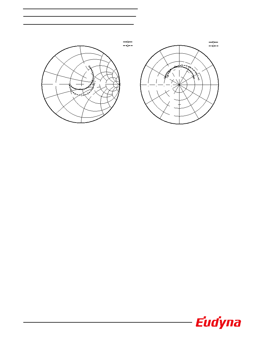
VDS =10V,
IDS = 0.65 IDSS (Typ.),
f = 13.75 ~ 14.5 GHz,
ZS=ZL=50 ohm
f = 14.5GHz,
f = 10 MHz
2-Tone Test
Pout = 28.0dBm S.C.L.
mA
mS
V
dB
%
-42
-45
-
dBc
dBm
V
gm
Vp
VGSO
P1dB
G1dB
Drain Current
-
2400
3000
mA
Idsr
IM3
add
Gain Flatness
-
-
±0.6
dB
G
Test Conditions
Unit
Limit
Typ.
Max.
Min.
ELECTRICAL CHARACTERISTICS (Ambient Temperature Ta=25
°C)
Channel to Case
Thermal Resistance
-
2.8
3.3
°C/W
Rth
G.C.P.: Gain Compression Point, S.C.L.: Single Carrier Level
CASE STYLE: IA
10V x Idsr x Rth
Channel Temperature Rise
-
-
80
°C
Tch
DESCRIPTION
The FLM1314-8F is a power GaAs FET that is internally matched for
standard communication bands to provide optimum power and gain in a
50 ohm system.
FEATURES
· High Output Power: P1dB = 39.0dBm (Typ.)
· High Gain: G1dB = 6.0dB (Typ.)
· High PAE:
add = 28% (Typ.)
· Low IM3 = -45dBc@Po = 28.0dBm
· Broad Band: 13.75 ~ 14.5GHz
· Impedance Matched Zin/Zout = 50
2
FLM1314-8F
X, Ku-Band Internally Matched FET
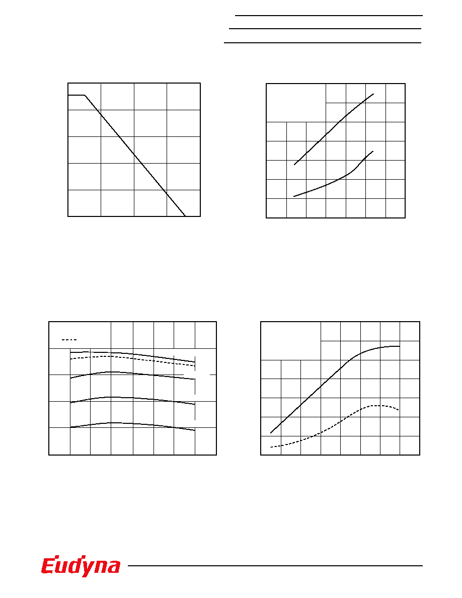
POWER DERATING CURVE
50
0
100
150
200
Case Temperature (
°C)
40
50
30
20
10
Total Power Dissipation (W)
OUTPUT POWER & IM3 vs. INPUT POWER
VDS = 10V
f1 = 14.5 GHz
f2 = 14.51 GHz
2-tone test
18
22
20
26
24
28
Input Power (S.C.L.) (dBm)
S.C.L.: Single Carrier Level
Output Power (S.C.L.) (dBc)
-30
-20
-40
-50
28
26
24
30
32
22
IM
3
(dBc)
IM3
Pout
13.75
14.00
14.25
14.50
36
34
38
40
Frequency (GHz)
Output Power (dBm)
OUTPUT POWER vs. FREQUENCY
VDS = 10V
P1dB
Pin = 35dBm
31dBm
29dBm
27dBm
24
26
28
30
32
34
36
34
30
32
36
38
40
30
20
10
Input Power (dBm)
Output Power (dBm)
add (%)
add
Pout
OUTPUT POWER vs. INPUT POWER
VDS = 10V
f = 14.125 GHz
4
FLM1314-8F
X, Ku-Band Internally Matched FET
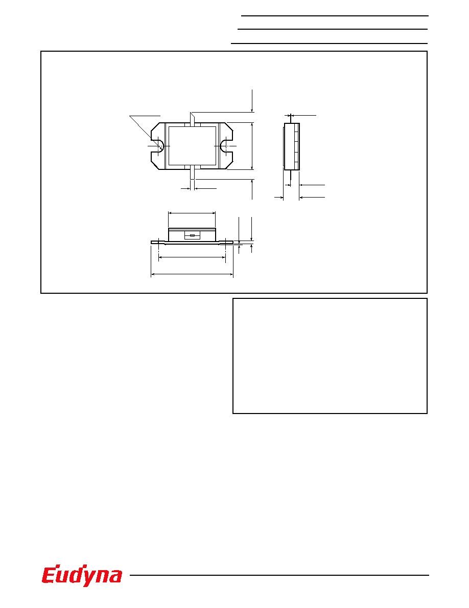
2-R 1.25
±0.15
(0.049)
0.5
(0.020)
8.1
(0.319)
13.0
±0.15
(0.512)
16.5
±0.15
(0.650)
3.2 Max.
(0.126)
1.8
±0.15
(0.071)
0.1
(0.004)
9.7
±
0.15
(0.382)
1.5 Min.
(0.059)
1.5 Min.
(0.059)
1.15
(0.045)
0.2 Max.
(0.008)
Case Style "IA"
Metal-Ceramic Hermetic Package
Unit: mm(inches)
1. Gate
2. Source (Flange)
3. Drain
4. Source (Flange)
1
2
3
4
Eudyna Devices Inc. products contain gallium arsenide
(GaAs) which can be hazardous to the human body and the environment.
For safety, observe the following procedures:
CAUTION
· Do not put this product into the mouth.
· Do not alter the form of this product into a gas, powder, or liquid
through burning, crushing, or chemical processing as these by-products
are dangerous to the human body if inhaled, ingested, or swallowed.
· Observe government laws and company regulations when discarding this
product. This product must be discarded in accordance with methods
specified by applicable hazardous waste procedures.
For further information please contact:
Eudyna Devices USA Inc.
2355 Zanker Rd.
San Jose, CA 95131-1138, U.S.A.
TEL: (408) 232-9500
FAX: (408) 428-9111
www.us.eudyna.com
Eudyna Devices Europe Ltd.
Network House
Norreys Drive
Maidenhead, Berkshire SL6 4FJ
United Kingdom
TEL: +44 (0) 1628 504800
FAX: +44 (0) 1628 504888
Eudyna Devices Asia Pte Ltd.
Hong Kong Branch
Rm. 1101, Ocean Centre, 5 Canton Rd.
Tsim Sha Tsui, Kowloon, Hong Kong
TEL: +852-2377-0227
FAX: +852-2377-3921
Eudyna Devices Inc.
Sales Division
1, Kanai-cho, Sakae-ku
Yokohama, 244-0845, Japan
TEL: +81-45-853-8156
FAX: +81-45-853-8170
Eudyna Devices Inc. reserves the right to change products and specifications
without notice. The information does not convey any license under rights of
Eudyna Devices Inc. or others.
© 2004 Eudyna Devices USA Inc.
Printed in U.S.A.