 | –≠–ª–µ–∫—Ç—Ä–æ–Ω–Ω—ã–π –∫–æ–º–ø–æ–Ω–µ–Ω—Ç: FMM5709X | –°–∫–∞—á–∞—Ç—å:  PDF PDF  ZIP ZIP |

FEATURES
Low Noise Figure : NF = 2.5dB ( Typ.) @ f=30GHz
High Associated Gain : Gas = 23dB ( Typ.) @f=30GHz
Broad Band : 17.5 ~ 32GHz
High Output Power : P1dB = 12.5dBm ( Typ. ) @f=30GHz
Impedance Matched Zin/Zout = 50
Edition 1.1
July 2004
1
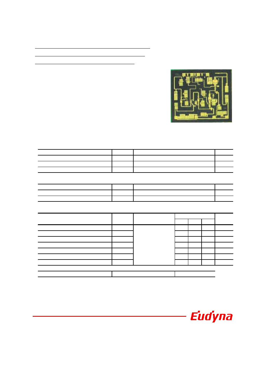
K / Ka Band Low Noise Amplifier MMIC
FMM5709X
DESCRIPTION
The FMM5709X is a LNA MMIC designed for applications in the
17.5 - 32 GHz frequency range. This product is well suited for satellite
communications, radio link, and applications where low noise and high
dynamic range are required.
Eudyna's stringent Quality Assurance Program assures the highest
reliability and consistent performance.
ABSOLUTE MAXIMUM RATING
Item
Symbol
Unit
Drain Voltage
V
DD
V
Input Power
P
in
dBm
Storage Temperature
T
stg
o
C
RECOMMENDED OPERATING CONDITIONS
Item
Symbol
Unit
Drain Voltage
V
DD
V
Operating Backside Temperature
T
op
o
C
ELECTRICAL CHARACTERISTICS (Ambient Temperature Ta=25
o
C)
Unit
Min.
Typ.
Max.
Noise Figure
NF
-
2.5
3.0
dB
Associated Gain
Gas
20
23
26
dB
Output Power at 1dB G.C.P.
P
1dB
-
12.5
-
dBm
Output 3rd order intercept point
OIP3
-
22.5
-
dBm
Drain Current at 1dB G.C.P.
Iddrf
-
60
75
mA
Input Return Loss
RLin
-
-10
-
dB
Output Return Loss
RLout
-
-10
-
dB
ESD
Note : Based on EIAJ ED-4701 C-111A(C=100pF, R=1.5kW)
Recommend
<=3
-45 to +85
Item
Symbol
Test Conditions
Rating
4
-3
-65 to +175
V
DD
=3V
f=30GHz
Z
L
=Z
S
=50ohm
Limits
Class 0
~ 199V

2
FMM5709X
K / Ka Band Low Noise Amplifier MMIC
NOISE FIGURE, ASSOCIATED GAIN
vs. FREQUENCY
V
DD
=3V
V
DD
=3V
P
1dB
, G
1dB
vs. FREQUENCY
OUTPUT POWER vs. INPUT POWER
V
DD
=3V
GAIN vs. INPUT POWER
V
DD
=3V
0
1
2
3
4
5
6
7
8
9
10
11
12
16 18 20 22 24 26 28 30 32 34 36 38 40
Frequency [GHz]
N
o
i
s
e
Fi
gur
e
[
d
B
]
0
5
10
15
20
25
30
A
s
so
c
i
at
e
d
G
a
i
n
[
d
B
]
NF
Gas
6
8
10
12
14
16
18
20
22
24
26
16 18 20 22 24 26 28 30 32 34 36
Frequency [GHz]
P
1d
B
[d
B
m
],
G
1d
B
[d
B
]
P1dB
G1dB
2
4
6
8
10
12
14
16
-22 -20 -18 -16 -14 -12 -10 -8 -6 -4 -2
Input Power [dBm]
Ou
t
p
u
t
P
o
we
r [
d
B
m
]
18GHz
22GHz
26GHz
30GHz
32GHz
14
16
18
20
22
24
26
-22 -20 -18 -16 -14 -12 -10 -8 -6 -4 -2
Input Power [dBm]
G
a
in
[
d
B
m
]
18GHz
22GHz
26GHz
30GHz
32GHz

3
K / Ka Band Low Noise Amplifier MMIC
FMM5709X
IMD PERFORMANCE
vs. TOTAL OUTPUT POWER
V
DD
=3V,
f=+10MHz
SMALL SIGNAL GAIN vs. FREQUENCY
V
DD
=3V
INPUT/OUTPUT RETURN LOSS
vs. FREQUENCY
V
DD
=3V
-70
-60
-50
-40
-30
-20
-10
0
-2
0
2
4
6
8
10 12 14 16
2-Tone Total Output Power [dBm]
I
n
t
e
r
m
odul
a
t
i
on D
i
s
t
or
t
i
on [
d
B
c
]
18GHz
22GHz
26GHz
30GHz
32GHz
IM
3
IM
5
-30
-25
-20
-15
-10
-5
0
5
10
15
20
25
30
0
5
10 15 20 25 30 35 40
Frequency [GHz]
S
m
a
ll S
i
g
n
a
l G
a
in
[
d
B
]
-30
-25
-20
-15
-10
-5
0
5
10
0
5
10 15 20 25 30 35 40
Frequency [GHz]
R
e
tu
r
n
L
o
s
s [d
B]
Input
Output

4
FMM5709X
K / Ka Band Low Noise Amplifier MMIC
S-Parameter
FREQ.
[MHz]
mag.
ang.
mag.
ang.
mag.
ang.
mag.
ang.
1000
0.959
-25.9
0.008
-156.9
0.001
-10.3
0.997
-19.1
2000
0.955
-51.0
0.019
154.9
0.001
-25.6
0.983
-39.1
3000
0.952
-75.9
0.035
65.7
0.001
-171.1
0.908
-59.1
4000
0.946
-99.9
0.031
-22.8
0.001
173.6
0.858
-75.7
5000
0.938
-123.2
0.018
-92.8
0.001
-1.3
0.816
-94.7
6000
0.930
-146.1
0.012
-102.3
0.001
-133.3
0.771
-112.0
7000
0.919
-168.5
0.009
-106.0
0.001
147.2
0.770
-137.7
8000
0.906
169.2
0.086
-80.9
0.000
131.7
0.586
-168.1
9000
0.890
146.8
0.233
175.3
0.001
161.3
0.415
176.9
10000
0.878
123.8
0.161
97.4
0.001
136.4
0.303
162.8
11000
0.860
98.9
0.138
156.8
0.001
89.5
0.217
156.2
12000
0.828
71.7
0.655
122.9
0.001
149.3
0.179
156.1
13000
0.769
40.9
1.666
71.2
0.002
13.5
0.165
154.9
14000
0.657
6.8
3.671
17.1
0.001
-15.4
0.162
149.5
15000
0.488
-27.9
7.153
-44.3
0.001
110.3
0.155
141.8
16000
0.319
-54.0
11.694
-111.8
0.002
-133.8
0.159
136.8
17000
0.222
-66.7
15.274
-179.8
0.001
-93.7
0.170
122.7
18000
0.210
-73.7
16.572
117.2
0.002
-103.6
0.158
109.1
19000
0.233
-91.4
16.251
61.8
0.002
83.2
0.146
91.6
20000
0.266
-112.2
15.490
13.4
0.003
159.7
0.115
80.0
21000
0.304
-134.9
15.034
-30.5
0.002
101.3
0.090
81.2
22000
0.342
-155.9
14.888
-71.8
0.002
122.4
0.079
90.9
23000
0.376
-177.1
14.901
-111.9
0.004
118.6
0.099
98.6
24000
0.402
162.2
15.063
-151.4
0.001
-5.9
0.130
94.2
25000
0.424
141.7
15.153
169.5
0.002
64.4
0.165
86.2
26000
0.441
123.4
15.263
130.8
0.005
43.5
0.196
69.3
27000
0.444
105.3
15.068
92.7
0.003
1.9
0.209
52.1
28000
0.437
88.5
14.910
55.4
0.004
24.1
0.222
33.2
29000
0.439
72.7
14.657
18.6
0.003
-31.2
0.221
14.3
30000
0.447
57.9
14.717
-18.1
0.003
-48.2
0.213
-1.9
31000
0.441
42.1
14.839
-54.9
0.002
6.4
0.202
-16.6
32000
0.457
25.4
14.982
-93.4
0.005
-11.1
0.179
-22.8
33000
0.453
5.3
15.122
-133.5
0.006
-132.4
0.196
-29.9
34000
0.414
-17.9
14.577
-176.8
0.008
103.9
0.238
-43.6
35000
0.365
-43.2
12.651
139.2
0.004
109.2
0.327
-69.5
36000
0.276
-67.3
10.093
97.6
0.005
161.1
0.355
-98.2
37000
0.188
-89.6
7.902
59.6
0.007
42.3
0.401
-127.4
38000
0.112
-107.1
6.067
26.8
0.006
63.4
0.416
-152.8
39000
0.053
-116.3
4.710
-3.9
0.010
23.4
0.446
179.1
40000
0.005
56.6
3.687
-31.8
0.010
16.7
0.459
160.2
V
DD
=3V
S11
S21
S12
S22

1.E+02
1.E+03
1.E+04
1.E+05
1.E+06
1.E+07
1.E+08
1.E+09
60
80
100 120 140 160 180 200 220 240 260 280
Channel Temperature (deg-C)
MT
T
F
(
h
r
s
)
Ea=1.02eV
Channel Temperature (
O
C)
5
K / Ka Band Low Noise Amplifier MMIC
FMM5709X
Unit
Tch
o
C
18
V
DD
=3V, I
DD
=60mA
THERMAL INFORMATION (REFERENCE DATA)
MTTF vs Tch

6
FMM5709X
K / Ka Band Low Noise Amplifier MMIC
Chip Size : 1650
±
30
m x 1440
±
30
m
Chip Thickness :
85
m
±
20
m
Bonding Pad Size :
RF-Pad :
80
m x 160
m
VDD-Pad : 80
m x 80
m
Chip Outline and Bonding Pad Locations (Dimension in Micro-Meters)
0
140
0
140
670
1130
1470
RF-in
680
RF-out
870
1650
1440
VDD

7
BONDING LAYOUT / EXTERNAL CIRCUIT
K / Ka Band Low Noise Amplifier MMIC
FMM5709X
100pF
1
F
V
DD
50
Line
50
Line
RF
Input
RF
Output
"Copper" is recommended material of the package or carrier.

DIE ATTACH
1) The die-attach station must have accurate temperature control, and an inert forming gas should
be used.
2)Chips should be kept at room temperature except during die-attach.
3) Place package or carrier on the heated stage.
4) Lightly grasp the chip edges by the longer side using tweezers.
Die attach conditions
Stage Temperature : 300 to 310 deg.C
Time : less than 15 seconds
AuSn Perform Volume : per next Figure
WIRE BONDING
The bonding equipment must be properly grounded. The following or equivalent equipment, tools,
materials, and conditions are recommended.
1) Bonding Equipment and Bonding Tool.
Bonding Equipment : West Bond Model 7400 (Manual Bonder)
Bonding Tool : CCOD-1/16-S-437-60-F-2010-MP (Deweyl)
2) Bonding Wire
Material : Hard or Half hard gold
Diameter : 0.7 to 1.0 mil
3) Bonding Conditions
Method : Thermal Compression Bonding with Ultrasonic Power
Tool Force : 0.196 N +/- 0.0196 N
Stage Temperature : 215 deg.C +/- 5 deg.C
Tool Heater : None
Ultrasonic Power Transmitter : West Bond Model 1400
Duration : 150 mS/Bond
0
100
200
300
400
500
0
1
2
3
4
5
Area of Chip Back Surface (mm^2)
Volume of Au-Sn Perform (10
-3
/mm
3
)
FMM5709X
K / Ka Band Low Noise Amplifier MMIC
8
FMM5709X

K / Ka Band Low Noise Amplifier MMIC
FMM5709X
9
Eudyna Devices USA Inc.
2355 Zanker Rd.
San Jose, CA 95131-1138, U.S.A.
TEL: (408) 232-9500
FAX: (408) 428-9111
www.us.eudyna.com
Eudyna Devices Europe Ltd.
Network House
Norreys Drive
Maidenhead, Berkshire SL6 4FJ
United Kingdom
TEL: +44 (0) 1628 504800
FAX: +44 (0) 1628 504888
Eudyna Devices Inc. reserves the right to change products and
specifications without notice.The information does not convey any
license under rights of Eudyna Devices Inc. or others.
CAUTION
Eudyna Devices Inc. products contain gallium arsenide
(GaAs) which can be hazardous to the human body and the
environment. For safety, observe the following procedures:
Do not put these products into the mouth.
Do not alter the form of this product into a gas, powder, or liquid
through burning, crushing, or chemical processing as these by-
products are dangerous to the human body if inhaled, ingested, or
swallowed.
Observe government laws and company regulations when
discarding this product. This product must be discarded in
accordance with methods specified by applicable hazardous waste
procedures.
Eudyna Devices Asia Pte. Ltd.
Hong Kong Branch
Rm.1101,Ocean Centre, 5 Canton Road
Tsim Sha Tsui, Kowloon, Hong Kong
TEL: +852-2377-0227
FAX: +852-2377-3921
Eudyna Devices Inc.
Sales Division
1, Kanai-cho, Sakae-ku
Yokohama, 244-0845, Japan
TEL +81-45-853-8156
FAX +81-45-853-8170
© 2004 Eudyna Devices USA Inc.
Printed in U.S.A.


