 | –≠–ª–µ–∫—Ç—Ä–æ–Ω–Ω—ã–π –∫–æ–º–ø–æ–Ω–µ–Ω—Ç: FPD5W1KX | –°–∫–∞—á–∞—Ç—å:  PDF PDF  ZIP ZIP |

Edition 1.1
July 2004
1
Avalanche Photodiode
FPD5W1KX
FEATURES
∑ Data rates up to 2.5Gb/s
∑ Operating temperature: -40∞c to 85∞C
∑ Photosensitive diameter: 30µm
∑ High cut-off frequency: 3.0GHz at M=5 and 10
∑ Large gain-bandwidth product: 40GHz
∑ Low dark current: 20nA
∑ Low multipled dark current: 3nA
∑ Low excess noise factor: 5 at M=10
APPLICATIONS
∑ 2.4 Gb/s optical transmission systems
DESCRIPTION
The FPD5W1KX is a wide bandwidth, high sensitivity avalanche photodiode (APD)
optimized for operation at 1550nm. This APD is designed for use in optical transmission
systems operating at a giga-bit-rate, above 2.4Gb/s, and for long transmission distances.
The APD chip has a photosensitive area diameter of 30µm. Fujitsu's advanced InP
material technology realizes a high reliability planar structure device with wide bandwidth
(large gain-bandwidth product) as well as low noise characteristics. A single-mode fiber is
aligned to a hermetically sealed APD through a highly stable optical coupling system.
Parameter
Symbol
Ratings
Unit
ABSOLUTE MAXIMUM RATINGS (Ta=25∞C, unless otherwise specified)
Min.
Max.
Storage Temperature
Tstg
∞C
+85
-40
Operating Temperature
∞C
Top
+85
-40
APD Forward Current
mA
IF
10
-
APD Reverse Voltage
V
VR
VB
-
APD Reverse Current
mA
I
R
3(peak)
0
Note: Since VB may vary from device-to-device, VB data is attached to each device for reference.

2
Avalanche Photodiode
FPD5W1KX
Parameter
OPTICAL & ELECTRICAL CHARACTERISTICS
(Ta=-40∞C to +85∞C, =1,310/1,550nm, unless otherwise specified)
Unit
Limits
Max.
Min.
Typ.
Test Conditions
Symbol
Ipo=2
µA
Maximum Multiplication
Factor
40
-
30
Mmax
dB
-
-
30
-
Optical Return Loss
ORL
APD Responsivity
A/W
-
0.8
0.85
-
0.8
0.92
-
0.75
-
-
-
0.7
= 1,310nm, M=1, 25∞C
= 1,550nm, M=1, 25∞C
= 1,310/1,550nm, M=1,
-40 ~ +85
∞C
= 1,610nm, M=1, 25∞C
R
Excess Noise Factor
6.3
4
(0.8)
-
(0.6)
M=10, f=30MHz, B=1MHz,
Ipo=2
µA
F
(x)
Capacitance
f=1MHz, VR=0.9 X VB
pF
0.7
-
0.55
Ct
-
-
-
-
800
70
∞C
-
1700
85
∞C
Dark Current
ID
nA
25
∞C
40
15
VR=0.9 x VB
2.0
2.5
1.5
Cut-off Frequency
RL=50
,
-3dB from 500kHz
GHz
GHz
GHz
fc
-
M=5, 10
-
M=20
M=3
-
3.0
3.0
3.0
-
-
-
-
160
70
∞C
-
340
85
∞C
Mulitiplied Dark Current
IDM
nA
25
∞C
10
1.5
M=1
Temperature Coefficient
of VB
V/
∞C
0.08
0.15
0.12
Note (1)
APD Breakdown Voltage
VB
V
40
60
50
ID = 10
µA, 25∞C
Note 1:
=VB/dTc
3
Avalanche Photodiode
FPD5W1KX
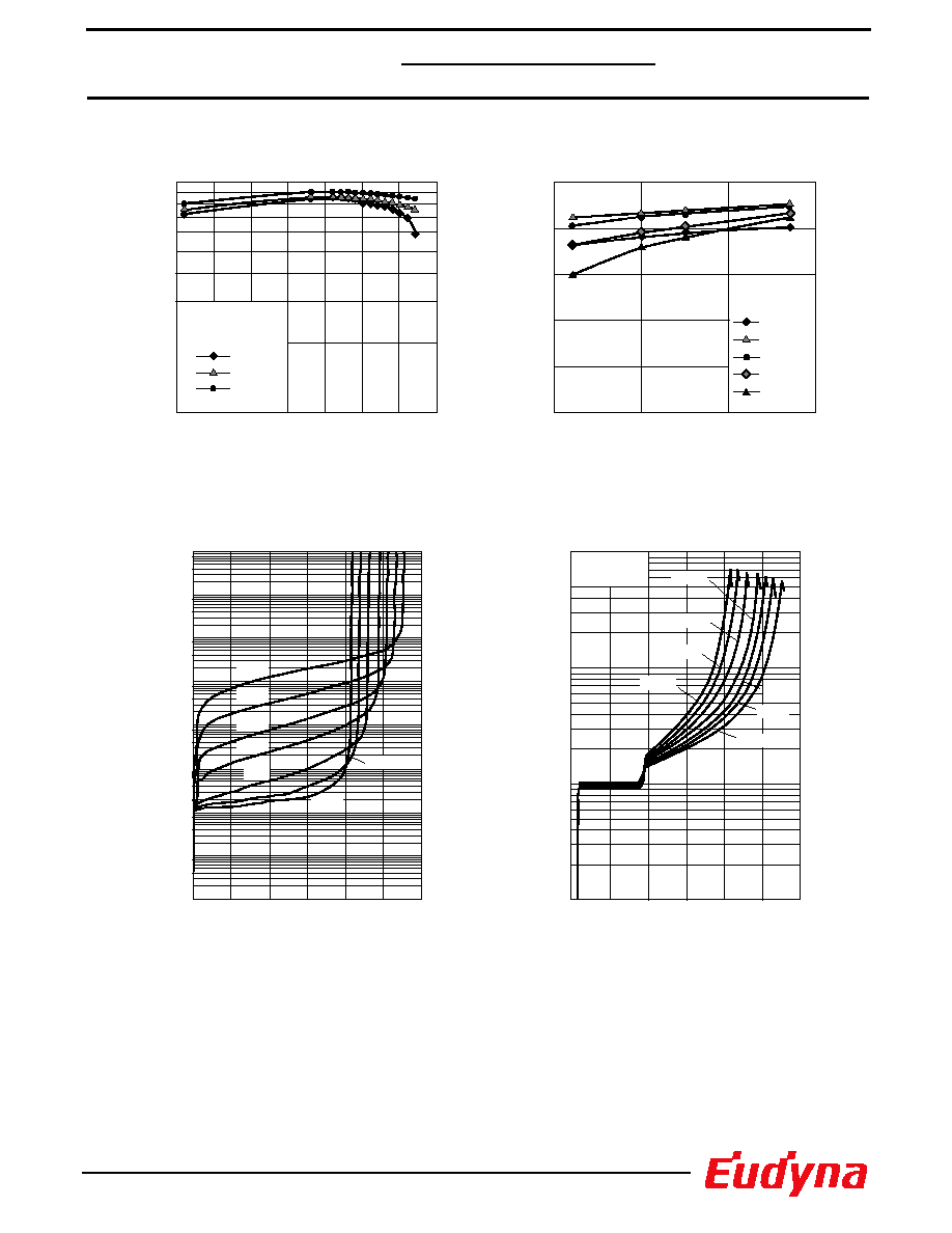
Fig. 1 Responsivity vs. Wavelength
Fig. 2 Responsivity vs. Temperature
Responsivity, (A/W)
1400
1300
1450 1500 1550 1600 1650
1350
0.1
1.0
Wavelength,
(nm)
Temperature, Ta (
∞C)
Fig. 3 Dark Current vs. Reverse Voltage
Dark Current, I
D
(A)
50
40
30
20
10
60
0
10-10
10-12
10-11
10-7
10-6
10-5
10-4
10-9
10-8
Reverse Voltage, VR (V)
25
∞C
45
∞C
-40
∞C
-25
∞C
65
∞C
85
∞C
0
∞C
-40
∞C
Pin=2
µW,
M=1
+85
∞C
+25
∞C
Responsivity, (A/W)
0
-50
50
100
0.0
0.2
0.4
0.6
0.8
1.0
1310nm
1480nm
1550nm
1600nm
1620nm
Pin=2
µW,
M=1
Fig. 5 Multiplication Characteristics
Multiplication Factor, M
50
40
30
20
10
60
0
0.1
10
100
1
Reverse Voltage, VR (V)
-40
∞C
45
∞C
65
∞C
85
∞C
25
∞C
0
∞C
-25
∞C
=1550nm,
Pin=2
µW
4
FPD5W1KX
10
100
0.1
1
Photocurrent at M=1, Ipo (
µA)
Fig. 6 Multiplication Factor vs. Photocurrent
Multiplication Factor, M
Relative Response (dB/div.)
1
1000
100
10
0
1
2
3
Frequency (GHz)
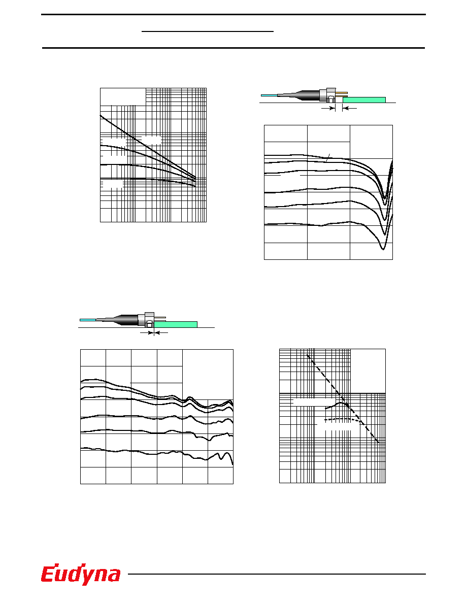
Fig. 7A Frequency Response
(Air Gap ~ 2mm)
0.98VB
0.95VB
0.9VB
Mmax
M=5
M=3
M=2
M=15
M=20
M=10
Ta=25∞C,
= 1,550nm
Ta = 25∞C,
= 1,550nm,
Pin=2
µW,
AC coupled,
RL = 50
10
100
0.1
1
Photocurrent at M=1, Ipo (
µA)
Fig. 8 Cutoff Frequency vs. Multiplication Factor
Multiplication Factor, M
0.1
100
10
1
Air Gap=0mm
Air Gap=2mm
(Air Gap ~ 2mm)
PCB
Relative Response (dB/div.)
0
1
2
3
4
5
6
Frequency (GHz)
Fig. 7B Frequency Response
(Air Gap ~ 0mm)
M=5
M=3
M=2
M=15
M=20
M=10
Ta = 25∞C,
= 1,550nm,
Pin=2
µW,
AC coupled,
RL = 50
Ta = 25∞C,
= 1,550nm,
Pin=2
µW,
AC coupled,
RL = 50
(Air Gap ~ 0mm)
PCB
Avalanche Photodiode

5
FPD5W1KX
Ta = 25∞C
(%/∞C)
(V/∞C)
Fig. 10 Excess Noise Factor
vs. Multiplication Factor
Capacitance, C
t (pF)
1
0.1
0.5
1
5
100
50
10
5
Fig. 9 Temperature Coefficient
vs. Breakdown Voltage
Excess Noise Factor, F
50
10
100
5
2
50
0
5
10
20
Reverse Voltage, VR (V)
Fig. 11 Capacitance vs. Reverse Voltage
Temperature Coeffcient of VB
50
45
60
55
40
0.3
0.2
0.1
0
Breakdown Voltage, VB (V)
Multiplication Factor, M
Ta = 25∞C,
= 1,550nm,
Ipo = 2µA,
f = 30 MHz,
B = 1 MHz
f = 1MHz
Avalanche Photodiode
6
FPD5W1KX
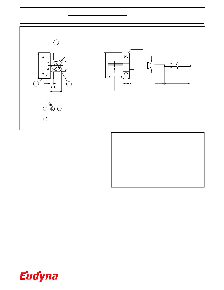
1
2
3
ANODE
CATHODE
CASE
4
2 - R 1.25
2 - C1.5
2.0
3.7
7.4
2
3
1
1000 MIN.
28 MAX.
17.0
¯
2.54
17.0
¯
6.0 MAX.
¯
0.9
3-
¯
0.35
12.7
7.4
10 MIN.
"KX" PACKAGE
UNIT: mm
Eudyna Devices Inc. products contain gallium arsenide
(GaAs) which can be hazardous to the human body and the environment.
For safety, observe the following procedures:
CAUTION
∑ Do not put this product into the mouth.
∑ Do not alter the form of this product into a gas, powder, or liquid
through burning, crushing, or chemical processing as these by-products
are dangerous to the human body if inhaled, ingested, or swallowed.
∑ Observe government laws and company regulations when discarding this
product. This product must be discarded in accordance with methods
specified by applicable hazardous waste procedures.
For further information please contact:
Eudyna Devices USA Inc.
2355 Zanker Rd.
San Jose, CA 95131-1138, U.S.A.
TEL: (408) 232-9500
FAX: (408) 428-9111
www.us.eudyna.com
Eudyna Devices Europe Ltd.
Network House
Norreys Drive
Maidenhead, Berkshire SL6 4FJ
United Kingdom
TEL: +44 (0) 1628 504800
FAX: +44 (0) 1628 504888
Eudyna Devices Asia Pte Ltd.
Hong Kong Branch
Rm. 1101, Ocean Centre, 5 Canton Rd.
Tsim Sha Tsui, Kowloon, Hong Kong
TEL: +852-2377-0227
FAX: +852-2377-3921
Eudyna Devices Inc.
Sales Division
1, Kanai-cho, Sakae-ku
Yokohama, 244-0845, Japan
TEL: +81-45-853-8156
FAX: +81-45-853-8170
Eudyna Devices Inc. reserves the right to change products and specifications
without notice. The information does not convey any license under rights of
Eudyna Devices Inc. or others.
© 2004 Eudyna Devices USA Inc.
Printed in U.S.A.
Avalanche Photodiode