 | –≠–ª–µ–∫—Ç—Ä–æ–Ω–Ω—ã–π –∫–æ–º–ø–æ–Ω–µ–Ω—Ç: FSU02LG | –°–∫–∞—á–∞—Ç—å:  PDF PDF  ZIP ZIP |
1
Edition 1.2
July 1999
FSU02LG
General Purpose GaAs FET
Item
Drain-Source Voltage
Gate-Source Voltage
Total Power Dissipation
Storage Temperature
Channel Temperature
Symbol
VDS
VGS
12
-5
750
-65 to +175
175
Note
V
V
mW
∞
C
∞
C
Ptot
Tstg
Tch
Condition
Unit
Rating
ABSOLUTE MAXIMUM RATING (Ambient Temperature Ta=25
∞
C)
Note: Mounted on Al2O3 board (30 x 30 x 0.65mm)
Fujitsu recommends the following conditions for the reliable operation of GaAs FETs:
1. The drain-source operating voltage (VDS) should not exceed 6 volts.
2. The forward and reverse gate currents should not exceed 1.4 and -0.2 mA respectively with
gate resistance of 2000
.
3. The operating channel temperature (Tch) should not exceed 145
∞
C.
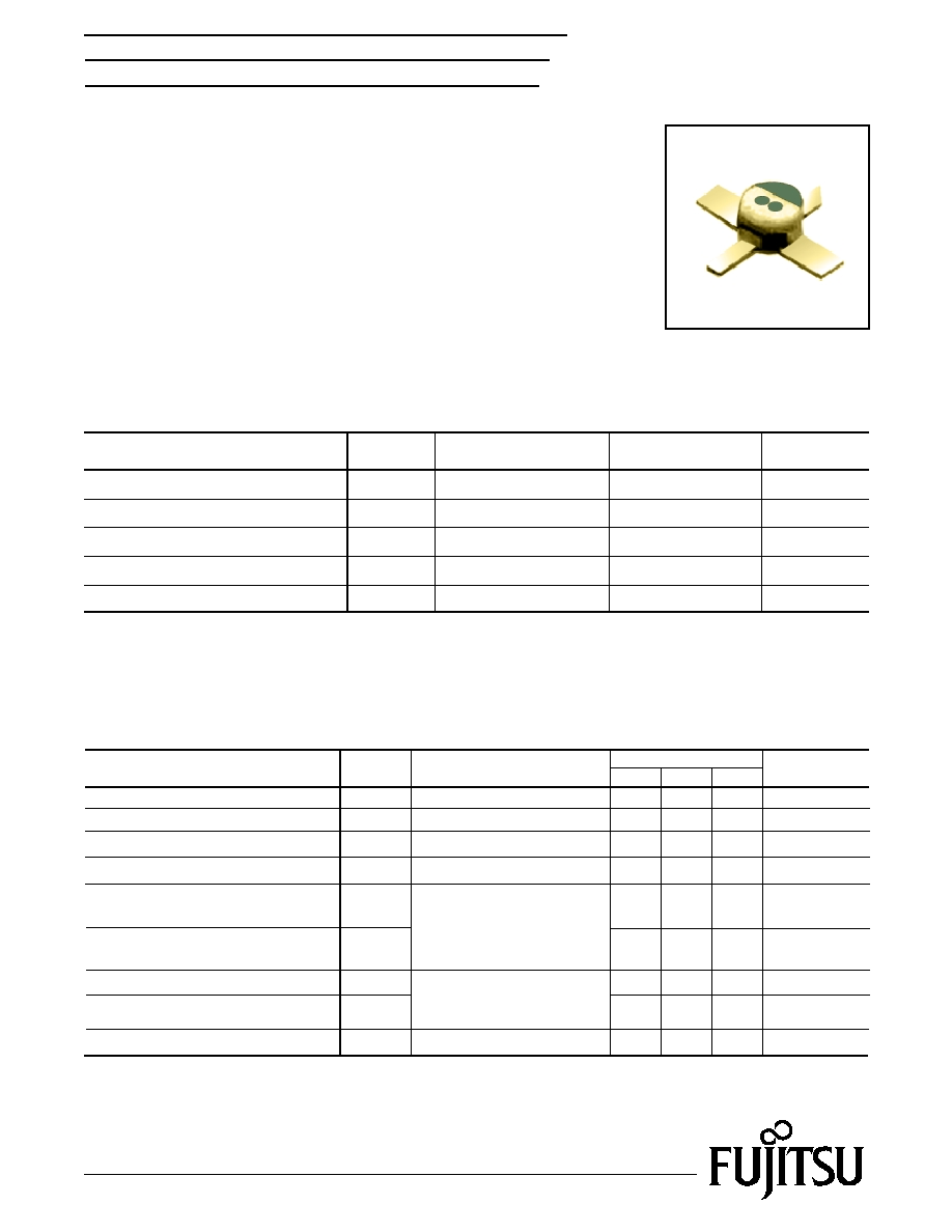
AVAILABLE CASE STYLES: LG
G.C.P.: Gain Compression Point
Item
Saturated Drain Current
Transconductance
Pinch-off Voltage
Gate Source Breakdown Voltage
Noise Figure
Output Power at 1dB
Gain Compression Point
Power Gain at 1dB
Gain Compression Point
Symbol
IDSS
80
110
150
-
100
-
-0.7
-1.2
-1.7
-5
-
-
16.0
17.0
-
-
1.5
-
22.0
23.0
-
VDS = 3V, IDS = 5.4mA
VDS = 3V, IDS =54mA
VDS = 3V, VGS = 0V
IGS = -5.4
µ
A
Channel to Case
VDS = 6V
IDS(DC)
=
80mA
f = 2GHz
VDS = 3V
IDS
=
20mA
f = 2GHz
mA
mS
V
dB
dB
dBm
V
gm
Vp
VGSO
P1dB
G1dB
NF
Associated Gain
-
17.5
-
dB
Gas
Thermal Resistance
-
150
200
∞
C/W
Rth
Test Conditions
Unit
Limit
Typ.
Max.
Min.
ELECTRICAL CHARACTERISTICS (Ambient Temperature Ta=25
∞
C)
Note: The RF parameters are measured on a lot basis by sample testing
at an AQL = 0.1%, Level-II inspection. Any lot failure shall be 100% retested.
DESCRIPTION
The FSU02LG is a high performance, low noise, GaAs FET designed for
PCS/PCN applications as a driver in the 2GHz band.
Fujitsu's stringent Quality Assurance Program assures the highest
reliability and consistent performance.
FEATURES
∑ High Output Power: P1dB = 23.0dBm (Typ.)@2GHz
∑ High Associated Gain: G1dB = 17.0dB (Typ.)@2GHz
∑ Low Noise Figure:
NF=1.5dB (Typ.)@f=2GHz
∑ Low Bias Conditions: VDS=3V, 20mA
∑ Cost Effective Hermetic Microstrip Package
∑ Tape and Reel Available

2
NOISE FIGURE vs. DRAIN-SOURCE CURRENT
ASSOCIATED GAIN vs. DRAIN-SOURCE CURRENT
VDS = 3V
f = 2.0 GHz
VDS = 3V
f = 2.0 GHz
20
60
80
40
20
60
80
40
Drain-Source Current (mA)
18.5
18
17.5
17
16.5
16
Associated Gain (dB)
Drain-Source Current (mA)
1.9
1.7
1.8
1.6
1.5
1.2
1.3
1.4
Noise Figure (dB)
OUTPUT POWER & IM3 vs. INPUT POWER
VDS = 6V
f = 2 GHz
f = +1 MHz
IDS = 80mA
5
2
-1
-4
-7
-10
-13
8
Total Input Power (dBm)
19
21
23
17
15
13
11
9
7
5
3
1
-1
-3
-5
-20
-10
-30
-40
-50
-60
Total Output Power (dBm)
IM
3
(dBc)
2-Tone
Single Tone
Pout
IM3
POWER DERATING CURVE
400
200
800
600
0
50
100
150
200
Case Temperature (
∞
C)
Total Power Dissipation (mW)
FSU02LG
General Purpose GaAs FET

3
S-PARAMETERS
VDS =6V, IDS = 80mA
FREQUENCY
S11
S21
S12
S22
(GHZ)
MAG
ANG
MAG
ANG
MAG
ANG
MAG
ANG
400
.993
-19.6
7.407
165.2
.012
76.3
.593
-9.4
600
.982
-29.3
7.259
157.9
.018
74.8
.589
-14.4
800
.971
-38.8
7.115
150.8
.023
68.3
.580
-19.2
1000
.952
-47.9
6.925
144.0
.029
62.7
.570
-23.6
1200
.938
-56.5
6.704
137.3
.032
59.1
.560
-27.8
1400
.921
-65.0
6.450
130.9
.037
54.8
.547
-31.7
1600
.899
-73.0
6.198
125.0
.041
51.3
.536
-36.5
1800
.880
-80.7
5.954
119.2
.043
47.6
.524
-39.3
2000
.836
-88.2
5.722
113.6
.046
42.2
.513
-42.9
2200
.843
-95.1
5.503
108.4
.048
40.1
.500
-46.3
2400
.829
-101.7
5.270
103.2
.051
38.2
.490
-49.7
2600
.818
-108.1
5.054
98.3
.053
34.5
.480
-53.3
2800
.802
-114.5
4.836
93.5
.055
30.0
.465
-56.5
3000
.781
-120.2
4.608
89.4
.054
27.1
.453
-58.2
3200
.774
-125.1
4.449
85.2
.055
27.6
.452
-60.8
3400
.766
-130.5
4.292
81.0
.055
23.5
.448
-64.0
3600
.758
-135.5
4.135
77.0
.056
23.0
.443
-66.8
3800
.753
-140.5
3.985
73.0
.057
21.5
.438
-70.0
4000
.747
-145.0
3.849
69.0
.059
20.4
.433
-73.2
+j250
+j100
+j50
+j25
+j10
0
-j10
-j25
-j50
-j100
-j250
S11
S22
180
∞
+90
∞
0
∞
-90
∞
S21
S12
SCALE FOR |S21|
4
.05
2
6
8
3.0
3.0
2.0
2.0
250
100
10
25
50
4 GHz
4 GHz
1.0 GHz
3.0
3.0
2.0
2.0
4 GHz
4 GHz
1.0 GHz
SCALE FOR |S12|
1.0 GHz
1.0 GHz
FSU02LG
General Purpose GaAs FET
Download S-Parameters, click here
4
For further information please contact:
FUJITSU COMPOUND SEMICONDUCTOR, INC.
2355 Zanker Rd.
San Jose, CA 95131-1138, U.S.A.
Phone: (408) 232-9500
FAX: (408) 428-9111
www.fcsi.fujitsu.com
FUJITSU MICROELECTRONICS EUROPE, GmbH
Quantum Devices Division
Network House
Norreys Drive
Maidenhead, Berkshire SL6 4FJ
Phone:+44 (0)1628 504800
FAX:+44 (0)1628 504888
Fujitsu Limited reserves the right to change products and specifications without notice.
The information does not convey any license under rights of Fujitsu Limited or others.
© 1998 FUJITSU COMPOUND SEMICONDUCTOR, INC.
Printed in U.S.A. FCSI0598M200
Fujitsu Compound Semiconductor Products contain gallium arsenide
(GaAs) which can be hazardous to the human body and the environment.
For safety, observe the following procedures:
CAUTION
∑ Do not put these products into the mouth.
∑ Do not alter the form of this product into a gas, powder, or liquid
through burning, crushing, or chemical processing as these by-products
are dangerous to the human body if inhaled, ingested, or swallowed.
∑ Observe government laws and company regulations when discarding this
product. This product must be discarded in accordance with methods
specified by applicable hazardous waste procedures.
0.5
(0.02)
1.0
(0.039)
1.3 Max
(0.051)
0.1
(0.004)
1.5
±
0.3
(0.059)
1.78
±
0.15
(0.07)
1.5
±
0.3
(0.059)
4.78
±
0.5
Case Style "LG"
Metal-Ceramic Package
Unit: mm(inches)
1. Gate
2. Source
3. Drain
4. Source
1.5
±
0.3
(0.059)
1.78
±
0.15
(0.07)
1.5
±
0.3
(0.059)
4.78
±
0.5
Gold Plated Leads
1
2
3
4
FSU02LG
General Purpose GaAs FET