 | –≠–ª–µ–∫—Ç—Ä–æ–Ω–Ω—ã–π –∫–æ–º–ø–æ–Ω–µ–Ω—Ç: GSM850 | –°–∫–∞—á–∞—Ç—å:  PDF PDF  ZIP ZIP |

FMM5321ZV
Quad-band Antenna Switch Module
GSM850 / GSM900 / DCS1800 / PCS1900 / GPRS Applications
Rev 1.1
April 20, 2005
1
Eudyna Devices Inc. Confidential
Features
∑ Quad-band, true SP6T PHEMT switch with integrated
decoder and low pass filter
∑ Low insertion loss solution over the frequencies from
824 to 960 MHz and 1710 to 1990 MHz with no
diplexer required
∑ Low cost, plastic mold package
∑
Small, low profile package: 4 x 4 x 0.85 mm
3
Applications
∑ Quad-band handset for GSM850/900 and
DCS1800/PCS1900
Description
The FMM5321ZV is a miniature 4 mm x 4 mm quad-
band GSM850/900, DCS1800, PCS1900 antenna switch
module that utilizes Eudyna's highly reliable PHEMT technology for Europe/US GSM and GPRS
handsets and wireless communication systems. The true SP6T PHEMT switch does not require a
diplexer, the component that causes additional insertion loss and yield degradation. The frequency
response is determined by built-in low pass filters, which simplify impedance matching with a power
amplifier.
Lead Free
4 mm x 4 mm x 0.85 mm
Module Package
Function Block Diagram
(Top View)
Packaging and Configuration
(Top View)
DCS in
GND
GND
GSM in
GND
GND
GND
GND
GND
Vctrl3
Vctrl2
Vctrl1
DC
S
R
x
GND
GND
GND
Vdd
AN
T
GND
D/P R
x
PCS Rx
GSM8
50 Rx
GN
D
GSM9
00 Rx
1
2
3
4
5
6
GND
LPF
7
8
9
10
11
12
GND
GND
GSM in
GND
GND
DCS in
Vctrl1
Vctrl2
GND
GND
GND
Vctrl3
GND
GND
GND
ANT
Vdd
GND
GND
DC
S
R
x
D/P R
x
GSM900 Rx
GSM850 Rx
PCS Rx
GND
18
17
16
15
14
13
21
20
19
22
23
24
LPF
SP
6T
S
w
i
t
c
h
De
c
o
de
r
FMM5321ZV
Quad-band Antenna Switch Module
GSM850 / GSM900 / DCS1800 / PCS1900 / GPRS Applications
Rev 1.1
April 20, 2005
2
Eudyna Devices Inc. Confidential
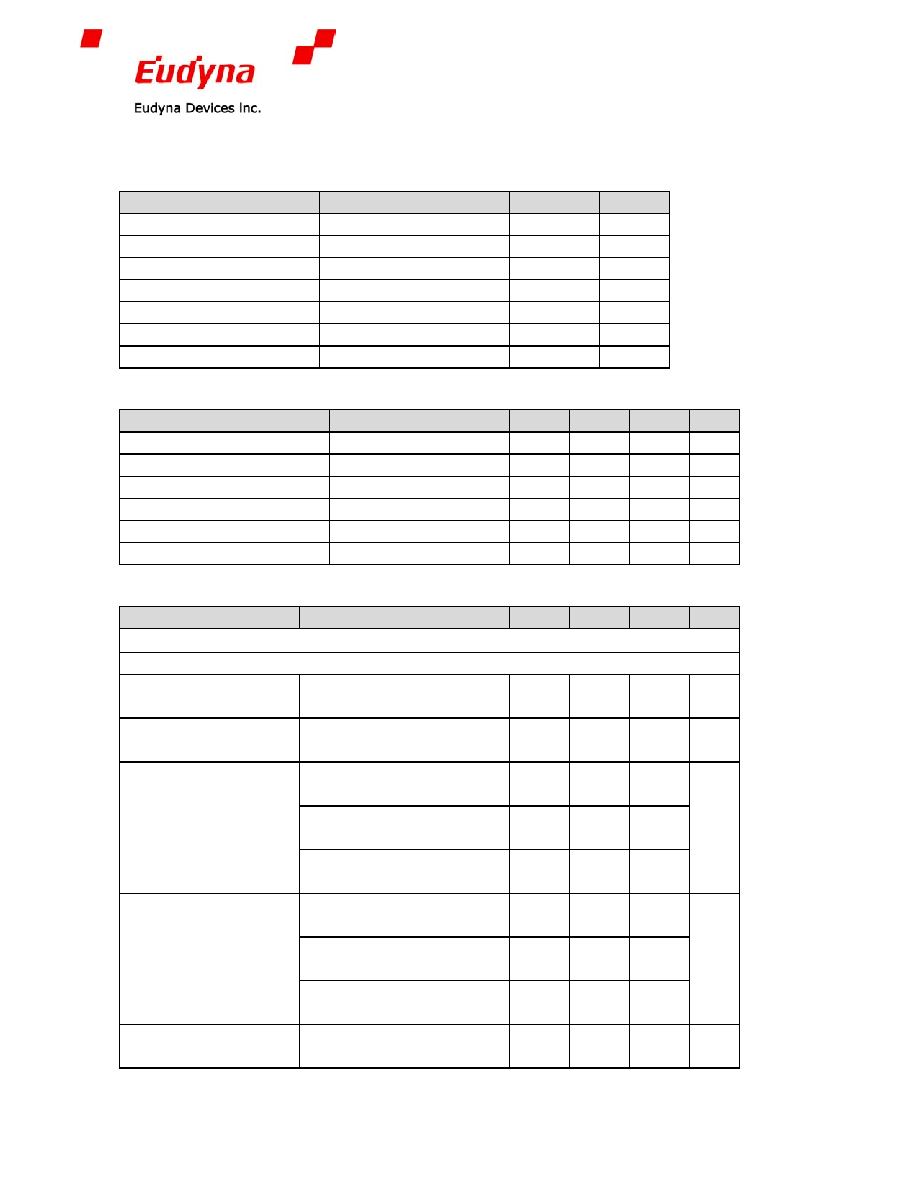
Absolute Maximum Ratings
Parameter
Condition/comments
Rating
Unit
Supply Voltage
5
V
Low Band Tx Input power
+36
dBm
High Band Tx Input power
+34
dBm
All Rx Input power
+12
dBm
Control Voltage Logic
Vdd+0.1
V
Storage case temperature
-35 to +85
∞C
Operating case temperature
-20 to +70
∞C
Recommended Operating Conditions (Ambient temperature 25∞C)
Parameter
Condition/Comments
Min
Typ
Max
Unit
Supply Voltage
Decoder supply
2.5
2.8
3.2
V
High
Control
Voltage
2.5 2.8 3.2 V
Low Control Voltage
-0.2
0
0.2
V
Low Band Tx Input power
35
dBm
High Band Tx Input power
33
dBm
All Rx Input power
10
dBm
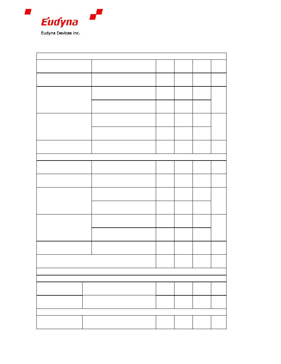
Electrical Specifications (Vdd=2.8 V, Vctrl=2.8 V, Tc=25∞C)
Parameter
Condition/Comments
Min
Typ
Max
Unit
TX Operation
GSM850 and GSM900 Tx @Pin=35 dBm
Insertion Loss
824 ≠ 915 MHz
-20 to 70 ∞C
1.05
1.2
1.4
dB
VSWR Tx
824 ≠ 915 MHz
-20 to 70 ∞C
1.5
1.7
1648 ≠ 1830 MHz
-20 to 70 ∞C
24
23
29
2472 ≠ 2745 MHz
-20 to 70 ∞C
22
17
24
Attenuation
3296 ≠ 3660 MHz
-20 to 70 ∞C
22
17
28
dB
1648 ≠ 1830 MHz
-20 to 70 ∞C
70
65
2472 ≠ 2745 MHz
-20 to 70 ∞C
68
63
Harmonics
3296 ≠ 3660 MHz
-20 to 70 ∞C
70
65
dBc
Port Isolation
GSM Tx to any Rx port
-20 to 70 ∞C
25
dB
FMM5321ZV
Quad-band Antenna Switch Module
GSM850 / GSM900 / DCS1800 / PCS1900 / GPRS Applications
Rev 1.1
April 20, 2005
3
Eudyna Devices Inc. Confidential
DCS1800 Tx @Pin=32 dBm
Insertion Loss
1710 ≠ 1785 MHz
-20 to 70 ∞C
1.4
1.6
1.7
dB
VSWR Tx
1710 ≠ 1785 MHz
-20 to 70 ∞C
1.5
1.7
3420 ≠ 3570 MHz
-20 to 70 ∞C
25
22
30
Attenuation
5130 ≠ 5355 MHz
-20 to 70 ∞C
16
16
18
dB
3420 ≠ 3570 MHz
-20 to 70 ∞C
67
63
Harmonics
5130 ≠ 5355 MHz
-20 to 70 ∞C
70
65
dBc
Port Isolation
DCS1800 Tx to any Rx port
-20 to 70 ∞C
25
dB
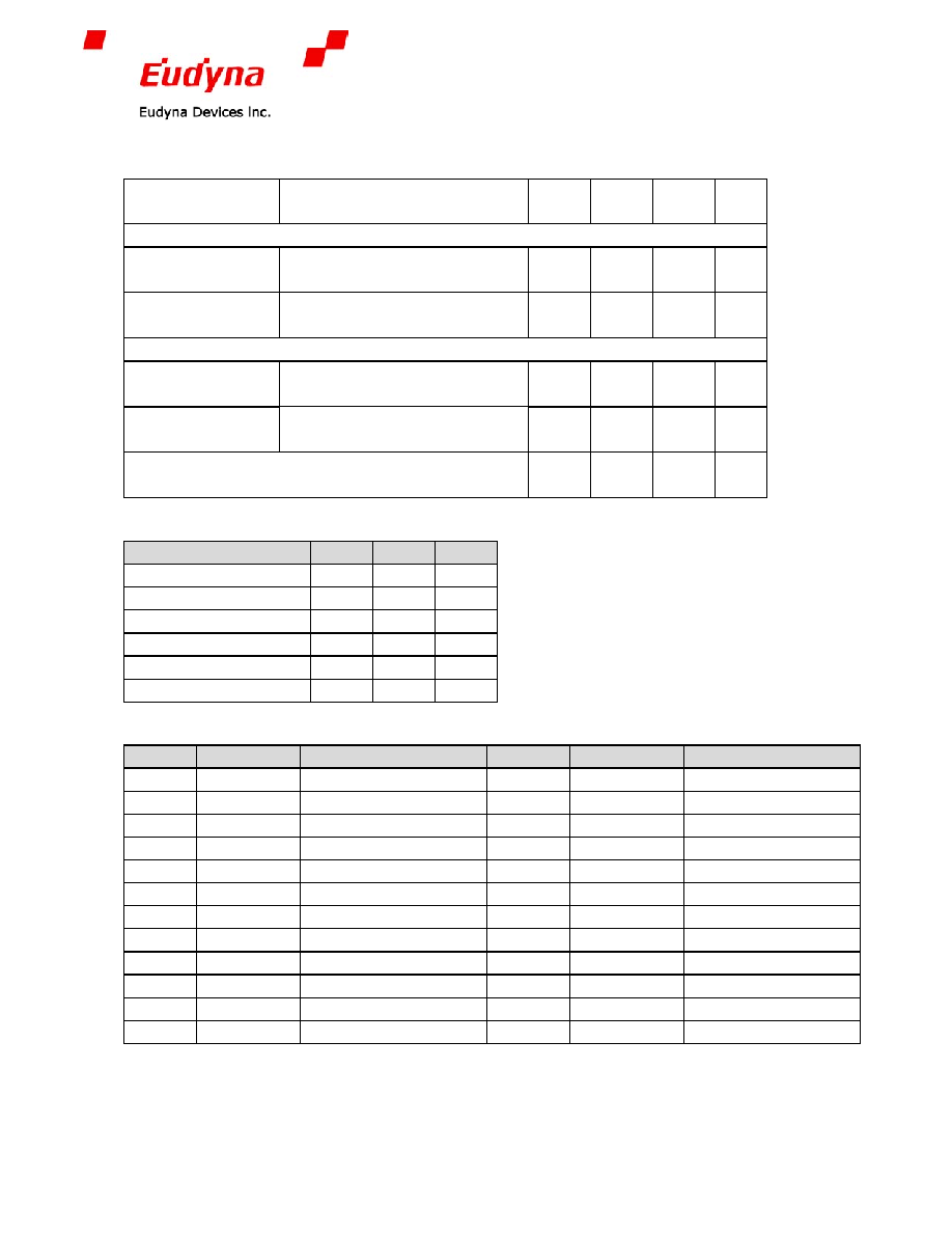
PCS1900 Tx @Pin=32 dBm
Insertion Loss
1850 ≠ 1910 MHz
-20 to 70 ∞C
1.5
1.7
1.9
dB
VSWR Tx
1850 ≠ 1910 MHz
-20 to 70 ∞C
1.5
1.7
3700 ≠ 3820 MHz
-20 to 70 ∞C
25
22
30
Attenuation
5550 ≠ 5730 MHz
-20 to 70 ∞C
19
17
22
dB
3700 ≠ 3820 MHz
-20 to 70 ∞C
70
63
Harmonics
5550 ≠ 5730 MHz
-20 to 70 ∞C
70
65
dBc
Port Isolation
PCS1900 Tx to any Rx port
-20 to 70 ∞C
25
dB
Current consumption Tx mode
-20 to 70 ∞C
500
950
uA
Rx Operation
GSM850 Rx
Insertion Loss
869 - 894 MHz, Pin=10 dBm
-20 to 70 ∞C
0.9
1.25
1.45
dB
VSWR Rx
869 - 894 MHz, Pin=10 dBm
-20 to 70 ∞C
1.5
GSM900 Rx
Insertion Loss
925 ≠ 960 MHz, Pin=10 dBm
-20 to 70 ∞C
1.0
1.35
1.55
dB
FMM5321ZV
Quad-band Antenna Switch Module
GSM850 / GSM900 / DCS1800 / PCS1900 / GPRS Applications
Rev 1.1
April 20, 2005
4
Eudyna Devices Inc. Confidential
VSWR Rx
925 ≠ 960 MHz, Pin=10 dBm
-20 to 70 ∞C
1.5
DCS1800 Rx
Insertion Loss
1805 ≠ 1880 MHz, Pin=10 dBm
-20 to 70 ∞C
1.2
1.5
1.7
dB
VSWR Rx
1805 ≠ 1880 MHz, Pin=10 dBm
-20 to 70 ∞C
1.5
PCS1900 Rx
Insertion Loss
1930 - 1990 MHz, Pin=10 dBm
-20 to 70 ∞C
1.3
1.5
1.7
dB
VSWR Rx
1930 - 1990 MHz, Pin=10 dBm
-20 to 70 ∞C
1.5
Current consumption Rx mode
-20 to 70 ∞C
600
1060
uA
Truth Table
Operation Mode
Vctrl1
Vctrl2
Vctrl3
GSM850 / GSM900 Tx
1
0
1/0
DCS1800 / PCS1900 Tx
1
1
1/0
GSM850
Rx
0 1 0
GSM900
Rx
0 0 1
DCS1800
Rx
0 0 0
PCS1900
Rx
0 1 1
Pin Configuration
Pin No.
Pin Name
Description
Pin No.
Pin Name
Description
1
DCS in
DCS/PCS Tx Port
13
GND
Ground
2
GND Ground 14
GND Ground
3 GND
Ground
15 Vctrl1
Control
1
4
GSM in
GSM850/GSM900 Tx Port
16
Vctrl2
Control 2
5 GND
Ground
17 Vctrl3
Control
3
6
GND Ground 18
GND Ground
7
DCS Rx
DCS Rx Port
19
GND
Ground
8
D/P Rxs
DCS/PCS Rx Shunt
20
ANT
Antenna Port
9
PCS Rx
PCS Rx Port
21
GND
Ground
10
GSM850 Rx
GSM850 Rx Port
22
Vdd
Decoder Vdd
11
GND Ground 23
GND Ground
12
GSM900 Rx
GSM900 Rx Port
24
GND
Ground
FMM5321ZV
Quad-band Antenna Switch Module
GSM850 / GSM900 / DCS1800 / PCS1900 / GPRS Applications
Rev 1.1
April 20, 2005
5
Eudyna Devices Inc. Confidential
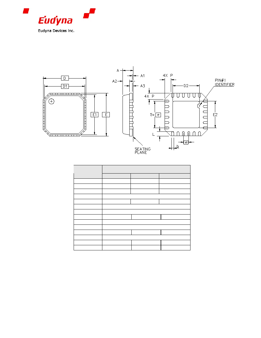
Package Dimensions
Measurement (mm)
Dimension
Symbol
Min
Nom
Max
A -
0.85
0.90
A1 0.00 0.01 0.05
A2 - 0.65
0.70
A3 0.20
REF
B 0.18
0.23 0.30
D 4.00
BSC
D1 3.75
BSC
D2 2.35 2.50 2.65
E 4.00
BSC
E1 3.75
BSC
E2 2.35 2.50 2.65
e 0.50
BSC
L 0.30
0.40
0.50
P 0.24 0.42 0.60
NOTE
This document is subject to change without notice.