
Technische Information / Technical Information
IGBT-Module
IGBT-Modules
BSM 50 GB 60 DLC
Hˆchstzul‰ssige Werte / Maximum rated values
Elektrische Eigenschaften / Electrical properties
Kollektor-Emitter-Sperrspannung
collector-emitter voltage
V
CES
600
V
T
c
= 80∞C
I
C,nom.
50
A
T
c
= 25∞C
I
C
75
A
Periodischer Kollektor Spitzenstrom
repetitive peak collector current
t
P
= 1ms, T
c
= 80∞C
I
CRM
100
A
Gesamt-Verlustleistung
total power dissipation
T
c
= 25∞C, Transistor
P
tot
280
W
Gate-Emitter-Spitzenspannung
gate-emitter peak voltage
V
GES
+/- 20V
V
Dauergleichstrom
DC forward current
I
F
50
A
Periodischer Spitzenstrom
repetitive peak forw. current
t
P
= 1ms
I
FRM
100
A
Grenzlastintegral der Diode
I
2
t - value, Diode
V
R
= 0V, t
p
= 10ms, T
vj
= 125∞C
I
2
t
450
A
2
s
Isolations-Pr¸fspannung
insulation test voltage
RMS, f= 50Hz, t= 1min.
V
ISOL
2,5
kV
Charakteristische Werte / Characteristic values
Transistor / Transistor
min.
typ.
max.
I
C
= 50A, V
GE
= 15V, T
vj
= 25∞C
-
1,95
2,45
V
I
C
= 50A, V
GE
= 15V, T
vj
= 125∞C
-
2,20
-
V
Gate-Schwellenspannung
gate threshold voltage
I
C
= 1,0mA, V
CE
= V
GE
, T
vj
= 25∞C
V
GE(th)
4,5
5,5
6,5
V
Eingangskapazit‰t
input capacitance
f= 1MHz, T
vj
= 25∞C, V
CE
= 25V, V
GE
= 0V
C
ies
-
2,2
-
nF
R¸ckwirkungskapazit‰t
reverse transfer capacitance
f= 1MHz, T
vj
= 25∞C, V
CE
= 25V, V
GE
= 0V
C
res
-
0,2
-
nF
V
CE
= 600V, V
GE
= 0V, T
vj
= 25∞C
-
1
500
µA
V
CE
= 600V, V
GE
= 0V, T
vj
= 125∞C
-
1
-
mA
Gate-Emitter Reststrom
gate-emitter leakage current
V
CE
= 0V, V
GE
= 20V, T
vj
= 25∞C
I
GES
-
-
400
nA
prepared by: Andreas Vetter
date of publication: 2000-04-26
approved by: Michael Hornkamp
revision: 1
V
CE sat
I
CES
Kollektor-Emitter S‰ttigungsspannung
collector-emitter saturation voltage
Kollektor-Emitter Reststrom
collector-emitter cut-off current
Kollektor-Dauergleichstrom
DC-collector current
1 (8)
BSM 50 GB 60 DLC
2000-02-08
Technische Information / Technical Information
IGBT-Module
IGBT-Modules
BSM 50 GB 60 DLC
Charakteristische Werte / Characteristic values
Transistor / Transistor
min.
typ.
max.
I
C
= 50A, V
CC
= 300V
V
GE
= ±15V, R
G
= 2,7
, T
vj
= 25∞C
t
d,on
-
40
-
ns
V
GE
= ±15V, R
G
= 2,7
, T
vj
= 125∞C
-
42
-
ns
I
C
= 50A, V
CC
= 300V
V
GE
= ±15V, R
G
= 2,7
, T
vj
= 25∞C
t
r
-
9
-
ns
V
GE
= ±15V, R
G
= 2,7
, T
vj
= 125∞C
-
10
-
ns
I
C
= 50A, V
CC
= 300V
V
GE
= ±15V, R
G
= 2,7
, T
vj
= 25∞C
t
d,off
-
120
-
ns
V
GE
= ±15V, R
G
= 2,7
, T
vj
= 125∞C
-
130
-
ns
I
C
= 50A, V
CC
= 300V
V
GE
= ±15V, R
G
= 2,7
, T
vj
= 25∞C
t
f
-
12
-
ns
V
GE
= ±15V, R
G
= 2,7
, T
vj
= 125∞C
-
21
-
ns
I
C
= 50A, V
CC
= 300V, V
GE
= 15V
R
G
= 2,7
, T
vj
= 125∞C, L
= 35nH
I
C
= 50A, V
CC
= 300V, V
GE
= 15V
R
G
= 2,7
, T
vj
= 125∞C, L
= 35nH
t
P
10µsec, V
GE
15V
T
vj
125∞C, V
CC
=360V, V
CEmax
= V
CES
-L
CE
∑di/dt
Modulinduktivit‰t
stray inductance module
L
CE
-
40
-
nH
Modul-Leitungswiderstand, Anschl¸sse - Chip
lead resistance, terminals - chip
T
c
= 25∞C
R
CC'+EE'
-
1,2
-
m
Charakteristische Werte / Characteristic values
Diode / Diode
min.
typ.
max.
Durchlaþspannung
I
F
= 50A, V
GE
= 0V, T
vj
= 25∞C
-
1,25
1,6
V
forward voltage
I
F
= 50A, V
GE
= 0V, T
vj
= 125∞C
-
1,20
-
V
I
F
= 50A, -di
F
/dt= 2900A/µsec
V
R
= 300V, V
GE
= -10V, T
vj
= 25∞C
I
RM
-
88
-
A
V
R
= 300V, V
GE
= -10V, T
vj
= 125∞C
-
92
-
A
I
F
= 50A, -di
F
/dt= 2900A/µsec
V
R
= 300V, V
GE
= -10V, T
vj
= 25∞C
Q
r
-
3,4
-
µC
V
R
= 300V, V
GE
= -10V, T
vj
= 125∞C
-
5,6
-
µC
I
F
= 50A, -di
F
/dt= 2900A/µsec
V
R
= 300V, V
GE
= -10V, T
vj
= 25∞C
E
rec
-
-
-
mJ
V
R
= 300V, V
GE
= -10V, T
vj
= 125∞C
-
1,5
-
mJ
-
Kurzschluþverhalten
SC Data
Fallzeit (induktive Last)
fall time (inductive load)
E
off
E
on
Einschaltverlustenergie pro Puls
turn-on energy loss per pulse
Abschaltverlustenergie pro Puls
turn-off energy loss per pulse
Einschaltverzˆgerungszeit (ind. Last)
turn on delay time (inductive load)
Anstiegszeit (induktive Last)
rise time (inductive load)
Abschaltverzˆgerungszeit (ind. Last)
turn off delay time (inductive load)
mJ
-
0,5
-
mJ
-
1,0
-
Abschaltenergie pro Puls
reverse recovery energy
A
V
F
R¸ckstromspitze
peak reverse recovery current
Sperrverzˆgerungsladung
recoverred charge
I
SC
-
225
2 (8)
BSM 50 GB 60 DLC
2000-02-08
Technische Information / Technical Information
IGBT-Module
IGBT-Modules
BSM 50 GB 60 DLC
Thermische Eigenschaften / Thermal properties
min.
typ.
max.
-
-
0,44
K/W
-
-
0,80
K/W
Ðbergangs-W‰rmewiderstand
thermal resistance, case to heatsink
pro Modul / per module
Paste
= 1W/m*K /
grease
= 1W/m*K
R
thCK
-
0,03
-
K/W
Hˆchstzul‰ssige Sperrschichttemperatur
maximum junction temperature
T
vj
-
-
150
∞C
Betriebstemperatur
operation temperature
T
op
-40
-
125
∞C
Lagertemperatur
storage temperature
T
stg
-40
-
125
∞C
Mechanische Eigenschaften / Mechanical properties
5
Nm
-15
+15
%
Al
2
O
3
275
mm
15
mm
8,5
Gewicht
weight
Transistor / transistor, DC
Diode / diode, DC
Geh‰use, siehe Anlage
case, see appendix
Innere Isolation
internal insulation
Anzugsdrehmoment f¸r mech. Befestigung
mounting torque
CTI
comperative tracking index
Kriechstrecke
creepage insulation
Luftstrecke
clearance
Innerer W‰rmewiderstand
thermal resistance, junction to case
Mit dieser technischen Information werden Halbleiterbauelemente spezifiziert, jedoch keine Eigenschaften zugesichert.
Sie gilt in Verbindung mit den zugehˆrigen Technischen Erl‰uterungen.
This technical information specifies semiconductor devices but promises no characteristics.
It is valid in combination with the belonging technical notes.
R
thJC
Schraube M6
screw M6
M1
g
180
G
3 (8)
BSM 50 GB 60 DLC
2000-02-08

Technische Information / Technical Information
IGBT-Module
IGBT-Modules
BSM 50 GB 60 DLC
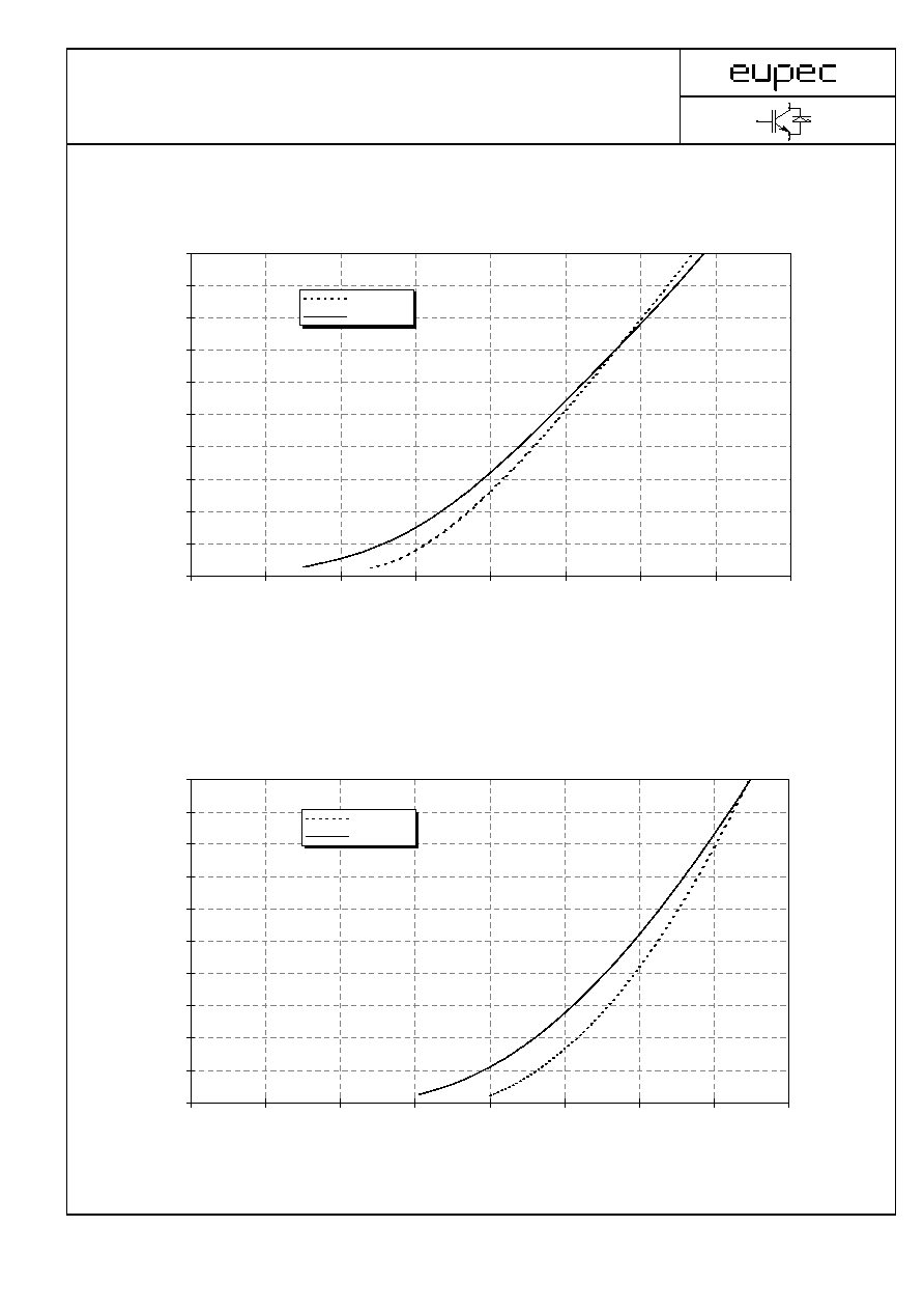
I
C
[A]
V
CE
[V]
I
C
[A]
V
CE
[V]
0
10
20
30
40
50
60
70
80
90
100
0,0
0,5
1,0
1,5
2,0
2,5
3,0
3,5
Tvj = 25∞C
Tvj = 125∞C
Ausgangskennlinie (typisch) I
C
= f (V
CE
)
Output characteristic (typical)
V
GE
= 15V
0
10
20
30
40
50
60
70
80
90
100
0,0
0,5
1,0
1,5
2,0
2,5
3,0
3,5
4,0
4,5
5,0
VGE = 8V
VGE = 9V
VGE = 10V
VGE = 12V
VGE = 15V
VGE = 20V
Ausgangskennlinienfeld (typisch) I
C
= f (V
CE
)
Output characteristic (typical)
T
vj
= 125∞C
4 (8)
BSM 50 GB 60 DLC
2000-02-08
Technische Information / Technical Information
IGBT-Module
IGBT-Modules
BSM 50 GB 60 DLC
I
C
[A]
V
GE
[V]
I
F
[A]
V
F
[V]
0
10
20
30
40
50
60
70
80
90
100
5
6
7
8
9
10
11
12
13
Tvj = 25∞C
Tvj = 125∞C
Ðbertragungscharakteristik (typisch) I
C
= f (V
GE
)
Transfer characteristic (typical)
V
CE
= 20V
0
10
20
30
40
50
60
70
80
90
100
0,0
0,2
0,4
0,6
0,8
1,0
1,2
1,4
1,6
Tvj = 25∞C
Tvj = 125∞C
Durchlaþkennlinie der Inversdiode (typisch) I
F
= f (V
F
)
Forward characteristic of inverse diode (typical)
5 (8)
BSM 50 GB 60 DLC
2000-02-08