 | –≠–ª–µ–∫—Ç—Ä–æ–Ω–Ω—ã–π –∫–æ–º–ø–æ–Ω–µ–Ω—Ç: D2601NH | –°–∫–∞—á–∞—Ç—å:  PDF PDF  ZIP ZIP |

Technische Information / Technical Information
Puls Power Abblockdiode
Puls Power Blocking Diode
D 2601 NH 90 T
Vorl‰ufige Daten
Preliminary Data
PM BIP / 2000-05-03 Keller
Release 2
Seite/page
N
1
Features:
∑
High surge current for Puls Power applications
∑
High di/dt at turn-off
∑
High reverse voltage
Elektrische Eigenschaften / Electrical properties
Hˆchstzul‰ssige Werte / Maximum rated values
Periodische Spitzensperrspannung
repetitive peak reverse voltage
T
vj
= -40∞C ... T
vj max
f = 50Hz
V
RRM
9000 V
Durchlaþstrom-Grenzeffektivwert
RMS forward current
T
C
= 60∞C, f = 50Hz
I
FRMSM
2900 A
Dauergrenzstrom
mean forward current
T
C
= 85∞C, f = 50Hz
t
C
= 60∞C, f = 50Hz
I
FAVM
1500
1850
A
A
t
vj
= 25∞C, t
rise
= 8µs, t
fall
= 20µs
V
R
= 1500V
I
FSM
80 kA
t
vj
= 40∞C, t
p
= 10ms
V
R
= 8500V
I
FSM
32 kA
Stoþstrom-Grenzwert
surge forward current
t
vj
= 25∞C, t
p
= 10ms
t
vj
= t
vj max
, t
p
= 10ms
I
FSM
47
45
kA
kA
Grenzlastintegral
I
2
t-value
t
vj
= 25∞C, t
p
= 10ms
t
vj
= t
vj max
, t
p
= 10ms
I
2
t
13,5 * 10
6
12,5 * 10
6
A
2
s
A
2
s
Charakteristische Werte / Characteristic values
Durchlaþspannung
forward voltage
t
vj
= t
vj max
, i
F
= 4000 A
v
F
max.
4,9 V
Schleusenspannung
threshold voltage
t
vj
= t
vj max
V
(TO)
1,04 V
Ersatzwiderstand
forward slope resistance
t
vj
= t
vj max
r
T
0,96 m
Durchlaþrechenkennlinie
500 A
i
F
5000 A
On-state characteristics for calculation
(
)
V
A B i
C
i
D i
F
F
F
F
= + +
+ +
ln
1
t
vj
= t
vj max
A
B
C
D
max.
0,71826748
0,00072434
≠0,00378418
0,02095741
Sperrstrom
reverse current
t
vj
= t
vj max,
v
R
= V
RRM
i
R
100 mA
R¸ckstromspitze
peak reverse recovery current
I
RM
1700
Sperrverzˆgerungsladung
recovered charge
t
vj
= t
vj max
V
R
= 2000V
R = 12Ohm, C = 1µF
i
FM
= 2500A, -di
F
/dt = 1000A/µs
Q
r
16000

Technische Information / Technical Information
Puls Power Abblockdiode
Puls Power Blocking Diode
D 2601 NH 90 T
Vorl‰ufige Daten
Preliminary Data
PM BIP / 2000-05-03 Keller
Release 2
Seite/page
N
2
Thermische Eigenschaften / Thermal properties
Innerer W‰rmewiderstand
thermal resistance, junction to case
beidseitig / two-sided, DC
Anode / anode, DC
Kathode /cathode, DC
R
thJC
max
max
max
0,0075
0,0141
0,0160
∞C/W
∞C/W
∞C/W
Ðbergangs-W‰rmewiderstand
thermal resistance, case to heatsink
K¸hlfl‰che / cooling surface
beidseitig / two-sided
einseitig / single sided
R
thCK
max
max
0,0025
0,005
∞C/W
∞C/W
Hˆchstzul‰ssige Sperrschichttemperatur
max. junction temperature
t
vj max
140 ∞C
Betriebstemperatur
operating temperature
t
c op
-40...+140 ∞C
Lagertemperatur
storage temperature
t
stg
-40...+140 ∞C
Mechanische Eigenschaften / Mechanical properties
Geh‰use, siehe Anlage
case, see appendix
Seite 3
Si - Element mit Druckkontakt
Si - pellet with pressure contact
76DNH90
Anpreþkraft
clamping force
F
36...52 KN
Gewicht
weight
G
typ
1200 G
Kriechstrecke
creepage distance
30 Mm
Luftstrecke
air distance
20 Mm
Feuchteklasse
humidity classification
DIN 40040
C
Schwingfestigkeit
vibration resistance
f = 50Hz
50 m/s
2
Mit dieser technischen Information werden Halbleiterbauelemente spezifiziert, jedoch keine Eigenschaften zugesichert. Sie gilt in Verbidung mit den zugehˆrigen technischen Erl‰uterungen.
This technical Information specifies semiconductor devices but promises no characteristics. It is valid in combination with the belonging technical notes.

Technische Information / Technical Information
Puls Power Abblockdiode
Puls Power Blocking Diode
D 2601 NH 90 T
Vorl‰ufige Daten
Preliminary Data
PM BIP / 2000-05-03 Keller
Release 2
Seite/page
N
3
Outline Drawing

Technische Information / Technical Information
Puls Power Abblockdiode
Puls Power Blocking Diode
D 2601 NH 90 T
Vorl‰ufige Daten
Preliminary Data
PM BIP / 2000-05-03 Keller
Release 2
Seite/page
N
4
On-State Characteristics ( v
F
)
upper limit of scatter range
0
500
1000
1500
2000
2500
3000
3500
4000
4500
5000
0
1
2
3
4
5
6
7
V
F
/ [V ]
T vj =140∞C
m ax.
Tvj =140∞C
typ.
Technische Information / Technical Information
Puls Power Abblockdiode
Puls Power Blocking Diode
D 2601 NH 90 T
Vorl‰ufige Daten
Preliminary Data
PM BIP / 2000-05-03 Keller
Release 2
Seite/page
N
5
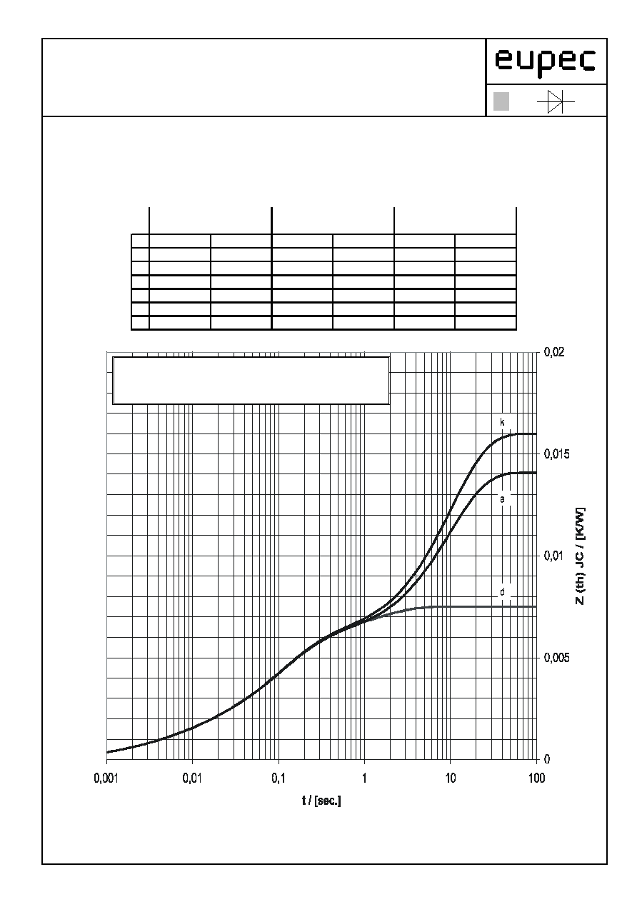
Transient thermal Impedance for constant-current
doppelseitige
K¸hlung
anodenseitige
K¸hlung
kathodenseitige
K¸hlung
r [K/W]
[s]
r [K/W]
[s]
r [K/W]
[s]
1 0,0015
1,38
0,0081
9,8
0,01
10,2
2 0,0023
0,185
0,0023
0,185
0,0023
0,185
3 0,0022
0,07
0,0022
0,07
0,0022
0,07
4 0,001
0,01
0,001
0,01
0,001
0,01
5 0,0005
0,0018
0,0005
0,0018
0,0005
0,0018
0,0075
-
0,0141
-
0,016
-
(
)
Z
R
e
thJC
thn
t
n
n
n
=
-
-
=
Â
1
1
/
max