Leistungsgleichrichterdioden
Power Rectifier Diodes
D 400 N
VWK July 1996
European Power-
Semiconductor and
Electronics Company
GmbH + Co. KG
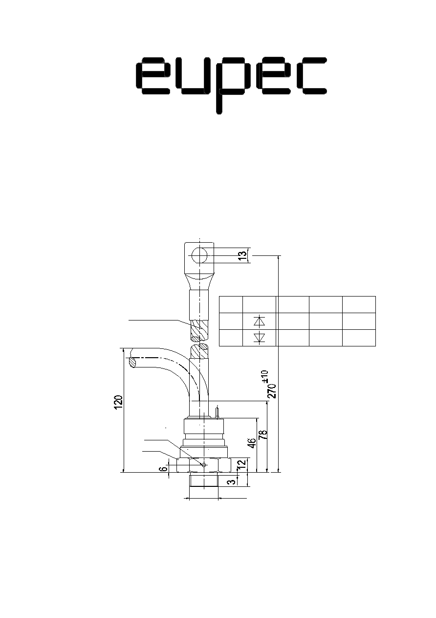
70mm≤ Cu
ш3,2 x 15
SW41
M24x 1,5
Type
N
K
Cathode
Rope
Case
Anode
Case
Rope
Prot. flex.
tubing
red
blue
Circuit
symbol
12,5

D 400 N
Elektrische Eigenschaften
Electrical properties
Hцchstzulдssige Werte
Maximum rated values
Periodische Spitzensperrspannung
repetitive peak reverse voltage
t
vj
= -40∞C... t
vj max
V
RRM
1200, 1600
V
1800, 2200
V
Stoяspitzensperrspannung
non-repetitive peak reverse voltage t
vj
= +25∞C... t
vj max
V
RSM
= V
RRM
+ 100
V
Durchlaяstrom-Grenzeffektivwert
RMS forward current
I
FRMSM
710
A
Dauergrenzstrom
mean forward current
t
c
= 130 ∞C
I
FAVM
400
A
t
c
= 121 ∞C
450
A
Stoяstrom-Grenzwert
surge forward current
t
vj
= 25∞C, t
p
= 10 ms
I
FSM
12,2
kA
t
vj
= t
vj max
, t
p
= 10 ms
9,7
kA
Grenzlastintegral
I
2
t-value
t
vj
= 25∞C, t
p
= 10 ms
I
2
t
744
kA
2
s
t
vj
= t
vj max
, t
p
= 10 ms
470,5
kA
2
s
Charakteristische Werte
Characteristic values
Durchlaяspannung
on-state voltage
t
vj
= t
vj max
, i
F
= 1,4 kA
V
T
max. 1,57
V
Schleusenspannung
threshold voltage
t
vj
= t
vj max
V
T(TO)
0,7
V
Ersatzwiderstand
slope resistance
t
vj
= t
vj max
r
T
0,58
m
Sperrstrom
reverse current
t
vj
= t
vj max
, V
R
= V
RRM
i
R
max. 40
mA
Thermische Eigenschaften
Thermal properties
Innerer Widerstand
thermal resistance, junction
= 180∞ sin
R
thJC
max. 0,098
∞C/W
to case
DC
max. 0,094
∞C/W
№bergangs-Wдrmewiderstand
thermal resistance,case to heatsink
ohne Anschluяlasche/without contact lug
R
thCK
max. 0,03
∞C/W
mit Anschluяlasche/with contact lug
max. 0,04
∞C/W
Hцchstzul.Sperrschichttemperatur
max. junction temperature
t
vj max
180
∞C
Betriebstemperatur
operating temperature
t
c op
-40...+180
∞C
Lagertemperatur
storage temperature
t
stg
-40...+180
∞C
Mechanische Eigenschaften
Mechanical properties
Si-Element mit Druckkontakt
Si-pellet with pressure contact
= 30 mm
Anzugsdrehmoment
tightening torque
Gehдuseform/case design B
M
60
Nm
Gewicht
weight
G
typ. 600
g
Kriechstrecke
creepage distance
21
mm
Feuchteklasse
humidity classification
DIN 40040
C
Schwingfestigkeit
vibration resistance
f = 50 Hz
50
m/s
2
Maяbild
outline
Seite/page
Polaritдt
polarity
Anode=Gehдuse/case

0
1
2
3
4
5
6
7
8
9
10
D400N_4
0
0,1
0,2
0,3
1a
2a
1b
1c
2b
D400N_6
0
14
12
10
8
6
4
2
0
0,1
0,2
0,3
D400N_5
1a
1b
2a
1c
2b
2c
14
12
10
8
6
4
2
0
0
0,5
1,0
1,5
2,0
D400N_1
2,0
1,5
1,0
0,5
2c
1,0
0,9
0,8
0,7
0,6
0,5
[kA]
I
F(0V)M
I
F(0V)M
[kA]
(normiert)
i≤dt
I
F(0V)M
v
R
I
F(0V)M
v
R
t [s]
v
F
[V]
t [s]
t
[ms]
p
[kA]
i
F
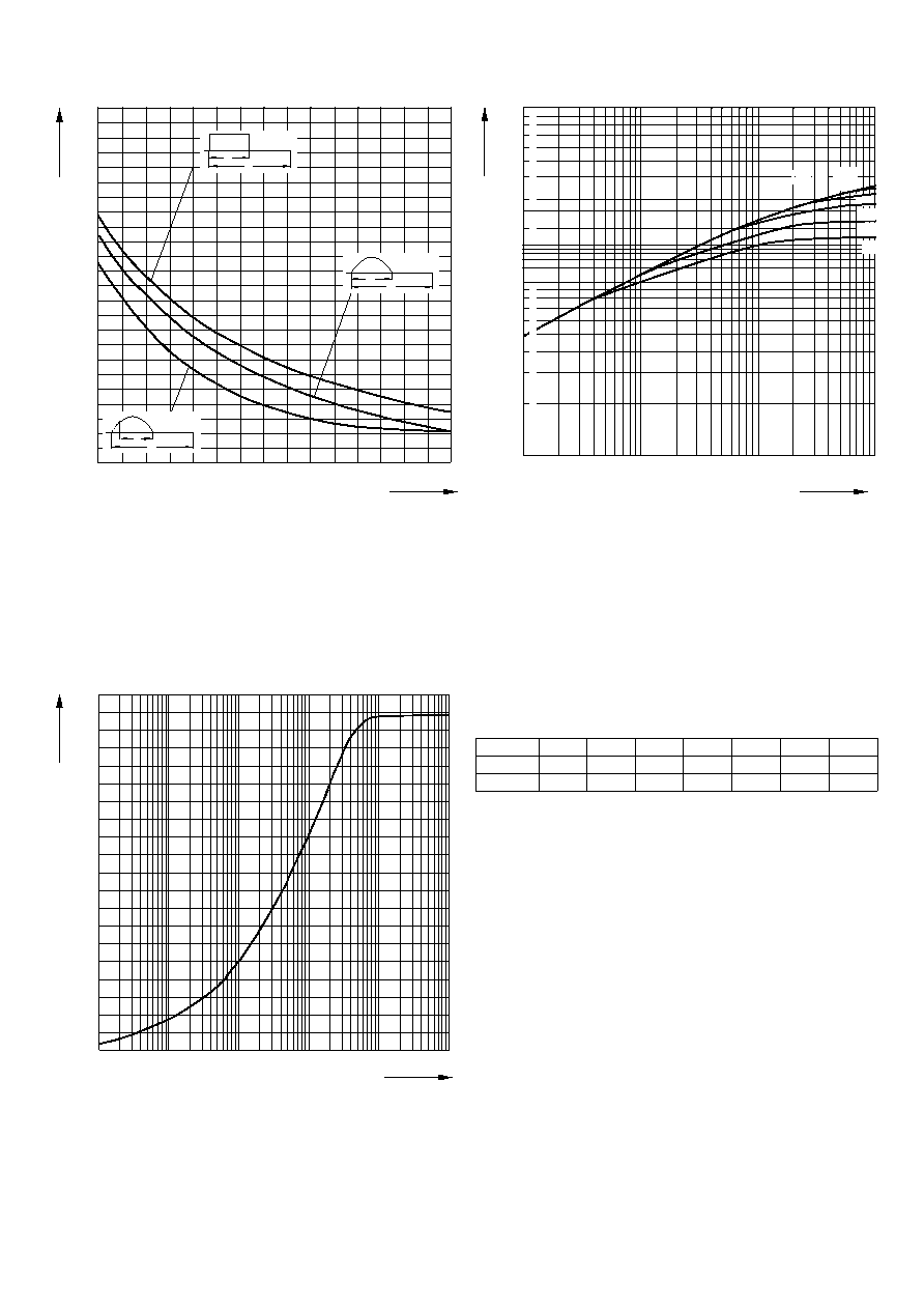
Bild / Fig. 2
Normiertes Grenzlastintegral / Normalized i≤t
i≤dt = f(t
p
)
t
vj
= 180 ∞C
t
vj
=
25 ∞C
Bild/Fig. 1
Grenzdurchlaяkennlinie
Limiting forward characteristic i
F
= f (v
F
)
Bild / Fig. 3
Grenzstrom / Maximum overload forward current I
F(0V)M
= f(t)
1 - I
FAV(vor)
= 0 A;
t
vj
= t
C
= 25 ∞C
2 - I
FAV(vor)
= 400 A;
t
C
= 130 ∞C; t
vj
= 180 ∞C
a - v
R
50 V
b - v
R
= 0,5 V
RRM
c - v
R
= 0,8 V
RRM
Bild / Fig. 4
Grenzstrom / Maximum overload forward current I
F(0V)M
= f(t)
1 - I
FAV(vor)
= 0 A;
t
vj
= t
C
= 25 ∞C
2 - I
FAV(vor)
= 400 A;
t
C
= 130 ∞C; t
vj
= 180 ∞C
a - v
R
50 V
b - v
R
= 0,5 V
RRM
c - v
R
= 0,8 V
RRM
D 400 N
0
D400N_2
0,10
0,08
0,06
0,04
0,02
10
-3
10
-2
10
-1
10
0
10
1
10
2
10
3
10
2
FM
[A]
D400N_7
1
10
100
0,1
800
400
200
100
50
9
8
7
6
5
4
3
2
9
8
7
6
5
4
3
2
1600
0
30
60
90
120
150
180
0,04
0,02
0,03
0,01
D400N_3
T
T
[
µ
As]
Q
r
Z
(th)JC
[∞C/W]
[∞C/W]
thJC
R
-di
F
/dt
[A/
µ
s]
t [s]
[∞el]
T
10
4
Bild / Fig. 5
Differenz zwischen den Wдrmewiderstдnden
fьr Pulsstrom und DC
Difference between the values of thermal resistance for
pulse current and DC
Parameter: Stromkurvenform / Current waveform
Bild / Fig. 6
Sperrverzцgerungsladung / Recovered charge Q
r
= f(-di
F
/dt)
t
vj =
t
vjmax
; v
R
0,5 V
RRM
; V
RM
= 0,8 V
RRM
Beschaltung / Snubber: C = 0,68 µF; R = 5,6
Parameter: Durchlaяstrom / Forward current i
FM
Analytische Funktion / Analytical function:
n
max
n=1
Analytische Elemente des transienten Wдrmewiderstandes Z
thJC
fьr DC
Analytical elements of transient thermal impedance Z
thJC
for DC
Bild / Fig. 7
Transienter innerer Wдrmewiderstand
Transient thermal impedance Z
thJC
= f(t), DC
1 - Beidseitige Kьhlung / Two-sided cooling
2 - Anodenseitige Kьhlung / Anode-sided cooling
3 - Kathodenseitige Kьhlung / Cathode-sided cooling
Z
thJC
=
R
thn
(1-EXP(-t/
n
))
Pos. n
R
thn
∞C/W
n
[s]
1
2
3
4
5
6
7
D 400 N
0,000087
0,000096
0,004051
0,00156
0,005142
0,0126
0,0223
0,133
0,06242
1,67
i