Leistungsgleichrichterdioden
Power Rectifier Diodes
D 428 N
VWK July 1996
ma
x. 7
Kathode
Cathode
Anode
¯3,5 x 2 tief / depth
beidseitig / on both sides
+0.1
8
,
5
1
4
1
,
1
¯ 23
¯ 23
4
4
1
1
9
,
5
2
1
,
1
European Power-
Semiconductor and
Electronics Company
GmbH + Co. KG

D 428 N
Elektrische Eigenschaften
Electrical properties
Hˆchstzul‰ssige Werte
Maximum rated values
Periodische Spitzensperrspannung
repetitive peak reverse voltage
t
vj
= -40∞C... t
vj max
V
RRM
800, 1200, 1400
V
1800, 2000
V
Stoþspitzensperrspannung
non-repetitive peak reverse voltage t
vj
= +25∞C... t
vj max
V
RSM
= V
RRM
+ 100
V
Durchlaþstrom-Grenzeffektivwert
RMS forward current
I
FRMSM
840
A
Dauergrenzstrom
mean forward current
t
c
= 139 ∞C
I
FAVM
430
A
1
)
t
c
= 130 ∞C
494
A
t
c
= 124 ∞C
535
Stoþstrom-Grenzwert
surge forward current
t
vj
= 25∞C, t
p
= 10 ms
I
FSM
7,7
kA
t
vj
= t
vj max
, t
p
= 10 ms
6
kA
Grenzlastintegral
I
2
t-value
t
vj
= 25∞C, t
p
= 10 ms
I
2
t
296,45
kA
2
s
t
vj
= t
vj max
, t
p
= 10 ms
180
kA
2
s
Charakteristische Werte
Characteristic values
Durchlaþspannung
on-state voltage
t
vj
= t
vj max
, i
F
= 1,6 kA
V
T
max. 1,76
V
Schleusenspannung
threshold voltage
t
vj
= t
vj max
V
T(TO)
0,81
V
Ersatzwiderstand
slope resistance
t
vj
= t
vj max
r
T
0,54
m
Sperrstrom
reverse current
t
vj
= t
vj max
, V
R
= V
RRM
i
R
max. 30
mA
Thermische Eigenschaften
Thermal properties
Innerer Widerstand
thermal resistance, junction
beidseitig/two-sided,
=180∞ sin R
thJC
max. 0,069 ∞C/W
to case
beidseitig/two sided, DC
max. 0,063 ∞C/W
Anode/anode,
=180∞ sin
max. 0,106 ∞C/W
Anode/anode, DC
max. 0,100 ∞C/W
Kathode/cathode,
=180∞ sin
max. 0,176 ∞C/W
Kathode/cathode, DC
max. 0,170 ∞C/W
Ðbergangs-W‰rmewiderstand
thermal resistance,case to heatsink beidseitig /two-sided
R
thCK
max. 0,015 ∞C/W
einseitig /single-sided
max. 0,030 ∞C/W
Hˆchstzul.Sperrschichttemperatur
max. junction temperature
t
vj max
180
∞C
Betriebstemperatur
operating temperature
t
c op
-40...+150
∞C
Lagertemperatur
storage temperature
t
stg
-40...+150
∞C
Mechanische Eigenschaften
Mechanical properties
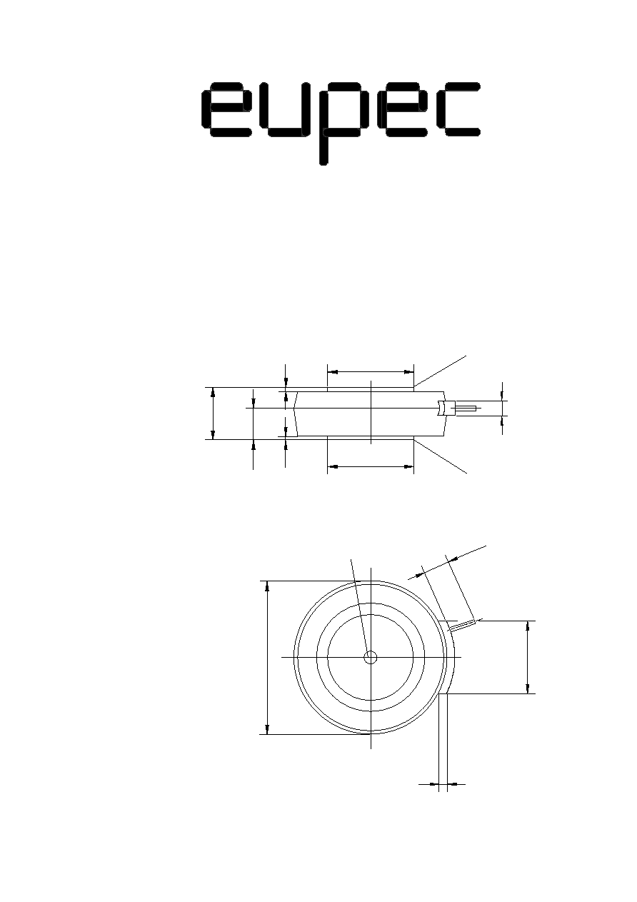
Si-Element mit Druckkontakt
Si-pellet with pressure contact
= 21 mm (
= 23 mm)
2
)
Anpreþkraft
clamping force
Geh‰useform/case design T
F
3,2...7,6
kN
Gewicht
weight
G
typ. 75
g
Kriechstrecke
creepage distance
25
mm
Feuchteklasse
humidity classification
DIN 40040
C
Schwingfestigkeit
vibration resistance
f = 50 Hz
50
m/s
2
Maþbild
outline
Seite/page
1
) Erg‰nzende Angabe zur Typenbezeichnung
additional value for type definition
2
) Durchmesser 23 mm nur f¸r V
RRM
= 2000 V
diameter 23 mm only for V
RRM
= 2000 V
0
1
2
3
4
5
6
7
8
9
10
D428N_4
0
0,5
1,0
1,5
2,0
D428N_1
2,5
2500
2000
1500
1000
500
0
0,1
0,2
0,3
1a
2a
1b
1c
2b
2c
D428N_6
0
7
6
5
4
3
2
1
0
0,1
0,2
0,3
D428N_5
2a
2b
2c
1a 1b
1c
+
+
7
6
5
4
3
2
1
8
[kA]
I
F(0V)M
I
F(0V)M
[kA]
(normiert)
i≤dt
I
F(0V)M
v
R
I
F(0V)M
v
R
t [s]
v
F
[V]
t [s]
1,0
0,8
0,6
0,4
0,2
0
t
[ms]
p
[A]
i
F
Bild / Fig. 2
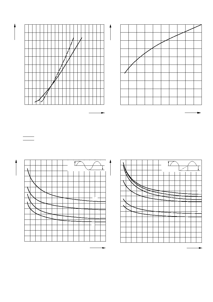
Normiertes Grenzlastintegral / Normalized i≤t
i≤dt = f(t
p
)
t
vj
= 180 ∞C
t
vj
= 25 ∞C
Bild/Fig. 1
Grenzdurchlaþkennlinie
Limiting forward characteristic i
F
= f (v
F
)
Bild / Fig. 3
Grenzstrom / Maximum overload forward current I
F(0V)M
= f(t)
1 - I
FAV(vor)
= 0 A; t
vj
= t
C
= 25 ∞C
2 - I
FAV(vor)
= 494 A; t
C
= 130 ∞C; t
vj
= 180 ∞C
a - v
R
50 V
b - v
R
= 0,5 V
RRM
c - v
R
= 0,8 V
RRM
Bild / Fig. 4
Grenzstrom / Maximum overload forward current I
F(0V)M
= f(t)
1 - I
FAV(vor)
= 0 A; t
vj
= t
C
= 25 ∞C
2 - I
FAV(vor)
= 494 A; t
C
= 130 ∞C; t
vj
= 180 ∞C
a - v
R
50 V
b - v
R
= 0,5 V
RRM
c - v
R
= 0,8 V
RRM
D 428 N
10
3
10
2
10
4
i
FM
[A]
D428N_7
1
10
100
0,1
800
400
200
100
50
9
8
7
6
5
4
3
2
9
8
7
6
5
4
3
2
25
0
30
60
90
120
150
180
0,04
0,02
0,03
0,01
0,05
0,06
D428N_3
0
0,20
0,18
0,14
0,12
0,10
0,08
0,06
0,04
0,02
D428N_2
1
2
3
10-3
10
-2
10
-1
10
0
10
1
10
2
T
T
[
µ
As]
Qr
Z
(th)JC
[∞C/W]
[∞C/W]
thJC
R
-di
F
/dt [A/
µ
s]
t [s]
[∞el]
T
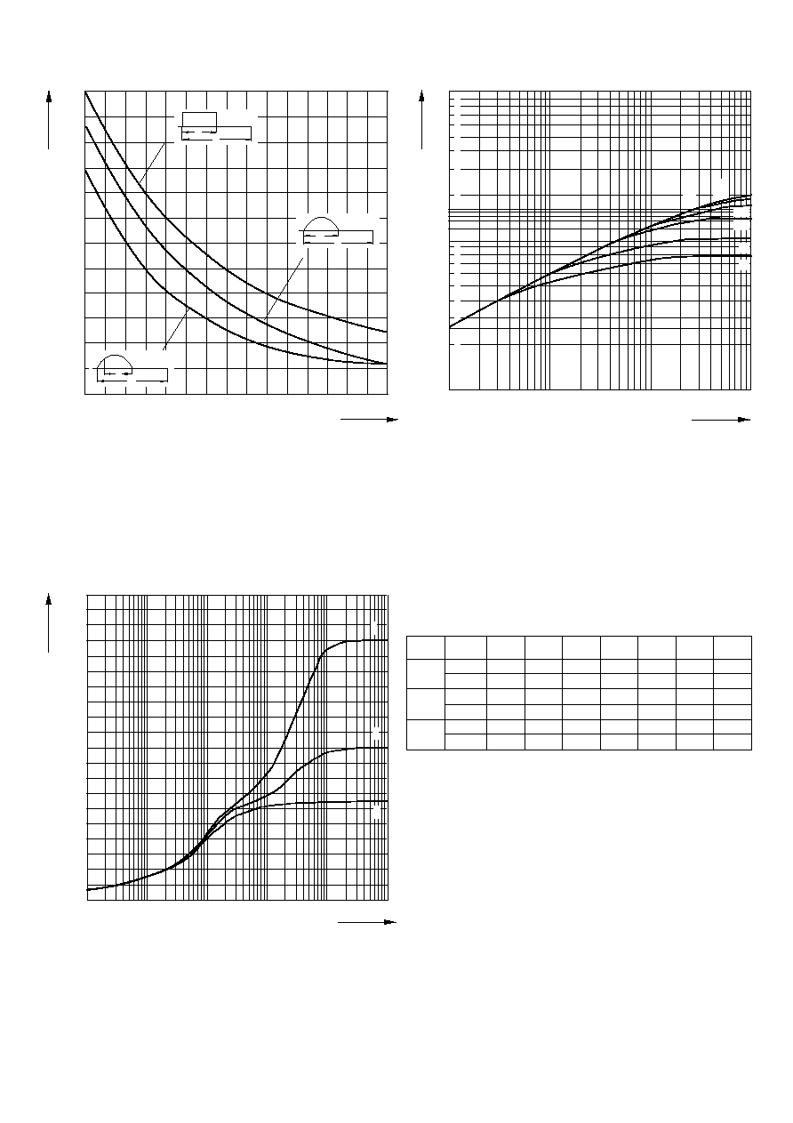
Bild / Fig. 5
Differenz zwischen den W‰rmewiderst‰nden
f¸r Pulsstrom und DC
Difference between the values of thermal resistance for
pulse current and DC
Parameter: Stromkurvenform / Current waveform
Bild / Fig. 6
Sperrverzˆgerungsladung / Recovered charge Q
r
= f(-di
F
/dt)
t
vj =
t
vjmax
; v
R
0,5 V
RRM
; V
RM
= 0,8 V
RRM
Beschaltung / Snubber: C = 0,47 µF; R = 8,2
Parameter: Durchlaþstrom / Forward current i
FM
n
max
n=1
Analytische Elemente des transienten W‰rmewiderstandes Z
thJC
f¸r DC
Analytical elements of transient thermal impedance Z
thJC
for DC
Bild / Fig. 7
Transienter innerer W‰rmewiderstand
Transient thermal impedance Z
thJC
= f(t), DC
1 - Beidseitige K¸hlung / Two-sided cooling
2 - Anodenseitige K¸hlung / Anode-sided cooling
3 - Kathodenseitige K¸hlung / Cathode-sided cooling
Z
thJC
= R
thn
(1-EXP(-t/
n
))
D 428 N
K¸hlg.
Cooling
Pos.
n
R
thn
∞C/W
n
[s]
R
thn
∞C/W
n
[s]
R
thn
∞C/W
n
[s]
1
2
3
1
2
3
4
5
6
7
1 - Beidseitige K¸hlung / Two-sided cooling
2 - Anodenseitige K¸hlung / Anode-sided cooling
3 - Kathodenseitige K¸hlung / Cathode-sided cooling
0,00063
0,000135
0,000632
0,000136
0,000626
0,000135
0,00635
0,00158
0,006388
0,00158
0,006574
0,0016
0,01052
0,0199
0,0128
0,022
0,0153
0,0274
0,0284
0,0815
0,0363
0,108
0,0325
0,113
0,0171
0,387
0,00758
0,699
0,115
3,46
Analytische Funktion / Analytical function
0,0363
3,78