 | –≠–ª–µ–∫—Ç—Ä–æ–Ω–Ω—ã–π –∫–æ–º–ø–æ–Ω–µ–Ω—Ç: D509S | –°–∫–∞—á–∞—Ç—å:  PDF PDF  ZIP ZIP |

Technische Information / Technical Information
Schnelle Gleichrichterdiode
Fast Diode
D 509 S 24...26
S
Elektrische Eigenschften / Electrical properties
Hˆchstzul‰ssige Werte / Maximum rated values
Periodische Spitzensperrspannung
T
vj
= - 25∞C...T
vj max
V
RRM
2400
V
repetitive peak forward reverse voltage
2600
V
Stoþspitzensperrspannung
T
vj
= + 25∞C...T
vj max
V
RSM
2500
V
non-repetitive peak reverse voltage
2700
V
Durchlaþstrom-Grenzeffektivwert
I
FRMSM
1050
A
RMS forward current
Dauergrenzstrom
T
C
=100∞C
I
FAVM
509
A
mean forward current
T
C
=74∞C
670
A
T
C
=107∞C
460
A
Stoþstrom-Grenzwert
T
vj
= 25∞C, tp = 10 ms
I
FSM
9000
A
surge foward current
T
vj
= T
vj max
, tp = 10 ms
7500
A
T
vj
= 25∞C, tp = 1 ms
21500
A
T
vj
= T
vj max
, tp = 1 ms
17900
A
Grenzlastintegral
T
vj
= 25∞C, tp = 10ms
I≤t
405000
A≤s
T
vj
= T
vj max
, tp = 10ms
281250
A≤s
T
vj
= 25∞C, tp = 1ms
231125
A≤s
I≤t-value
T
vj
= T
vj max
, tp = 1ms
160205
A≤s
Charakteristische Werte / Characteristic values
Durchlaþspannung
T
vj
= T
vj max
, i
F
= 2000 A
v
F
max.
2,7
V
forward voltage
Schleusenspannung
T
vj
= T
vj max
V
(TO)
1
V
threshold voltage
Ersatzwiderstand
T
vj
= T
vj max
r
T
0,8
m
forward slope resistance
Typischer Wert der Durchlaþverzˆgerungsspannung
IEC 747-2
V
FRM
typ
21
V
1)
typical value of forward recovery voltage
T
vj
= T
vj max
di
F
/dt=50A/µs, v
R
=0V
Durchlaþverzˆgerungszeit
IEC 747-2, Methode / method II
t
fr
typ
5,8
µs
1)
forward recovery time
T
vj
= T
vj max,
i
FM
=2000A
di
F
/dt=50 A/µs, v
R
=0V
Sperrstrom
T
vj
= 25∞C, v
R
=V
RRM
i
R
max.
16
mA
reverse current
T
vj
= T
vj max
, v
R
= V
RRM
max.
160
mA
R¸ckstromspitze
DIN IEC 747-2, T
vj
=T
vj max
I
RM
138
A
1)
peak reverse recovery current
i
FM
=670A,-di
F
/dt=50A/µs
v
R
=100V, v
RM<
=200 V
Sperrverzˆgerungsladung
DIN IEC 747-2, T
vj
=T
vj max
Q
r
760
µAs
1)
recovered charge
i
FM
=670 A,-di
F
/dt=50A/µs
v
R
=100V, v
RM<
=200 V
Sperrverzˆgerungszeit
DIN IEC 747-2, T
vj
=T
vj max
t
rr
7,3
µs
1)
reverse recovered time
i
FM
=670A,-di
F
/dt=50A/µs
v
R
=100 V; v
RM<
=200V
Sanftheit
T
vj
= T
vj max
SR
µs/A
2)
Softness
i
FM
=A,-di
F
/dt=A/µs
v
R
<=0,5 V
RRM
, v
RM
=0,8 V
RRM
1) Richtwert f¸r obere Streubereichsgrenze / Upper limit of scatter range (standard value)
2) Richtwert f¸r untere Streubereichsgrenze / Lower limit of scatter range (standard value)
SZ-M / 26.02.87
Seite/page 1

Technische Information / Technical Information
Schnelle Gleichrichterdiode
Fast Diode
D 509 S 24...26
S
Thermische Eigenschaften / Thermal properties
Innerer W‰rmewiderstand
K¸hlfl‰che / cooling surface
R
thJC
thermal resitance, junction to case
beidseitig / two-sided,
=180∞sin
max. 0,049
∞C/W
beidseitig / two-sided, DC
max. 0,045
∞C/W
Anode / anode,
=180∞sin
max. 0,086
∞C/W
Anode / anode, DC
max. 0,082
∞C/W
Kathode / cathode,
=180∞sin
max. 0,104
∞C/W
Kathode / cathode, DC
max. 0,100
∞C/W
Ðbergangs- W‰rmewiderstand
K¸hlfl‰che / cooling surface
R
thCK
thermal resitance, case to heatsink
beidseitig / two-sided
max. 0,005
∞C/W
einseitig / single-sided
max. 0,010
∞C/W
Hˆchstzul‰ssige Sperrschichttemperatur
T
vj max
150
∞C
max. junction temperature
Betriebstemperatur
T
c op
-40...+150
∞C
operating temperature
Lagertemperatur
T
stg
-40...+150
∞C
storage temperature
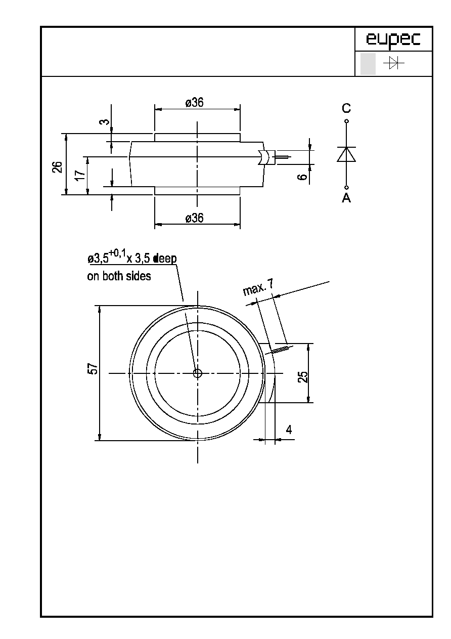
Mechanische Eigenschaften / Mechanical properties
Geh‰use, siehe Anlage
Seite 3
case, see appendix
page 3
Si-Element mit Druckkontakt
Durchmesser/diameter 30mm
Si-pellet with pressure contact
Anpreþkraft
F
6...14,5
kN
clamping force
Gewicht
G
typ.
270
g
weight
Kriechstrecke
28
mm
creepage distance
Feuchteklasse
DIN 40040
C
humidity classification
Schwingfestigkeit
f = 50Hz
5x9,81
m/s≤
vibration resistance
Mit dieser technischen Information werden Halbleiterbauelemente spezifiziert, jedoch keine Eigenschaften zugesichert. Sie gilt
in Verbindung mit den zugehˆrigen Technischen Erl‰uterungen./ The technical Information specifies semiconductors devices but
promises no characteristics. It is valid in combination with the belonging technical notes.
SZ-M / 26.02.87
Seite/page 2
Technische Information / Technical Information
Schnelle Gleichrichterdiode
Fast Diode
D 509 S 24...26
S
SZ-M / 26.02.87
Seite/page 3
Technische Information / Technical Information
Schnelle Gleichrichterdiode
Fast Diode
D 509 S24...26
S
K¸hlung
Analytische Elemente des transienten W‰rmewiderstandes Z
thJC
f¸r DC
cooling
Analytical ementes of transient thermal impedance Z
thJC
for DC
Pos.n
1
2
3
4
5
6
7
beidseitig
R
thn
[∞C/W]
0,00025
0,00457
0,00502
0,0166
0,0135
two-sided
n
[s]
0,000298
0,00243
0,021
0,113
0,76
anodenseitig
R
thn
[∞C/W]
0,0002
0,00474
0,00707
0,0203
0,00939
anode-sided
n
[s]
0,000247
0,00244
0,0265
0,177
4,3
kathodenseitig
R
thn
[∞C/W]
0,00018
0,00462
0,00726
0,0193
0,0205
cathode-sided
n
[s]
0,000232
0,00236
0,026
0,172
3,94
n
max
Analytische Funktion / analytical function : Z
thJC
=
=
R
thn
( 1 - EXP ( - t /
n
))
n=1
SZ-M / 26.02.87
Seite/page 4
0,04814
10,8
0,00506
2,16
0,0403
7,7
Technische Information / Technical Information
Schnelle Gleichrichterdiode
Fast Diode
D 509 S 24...26
S
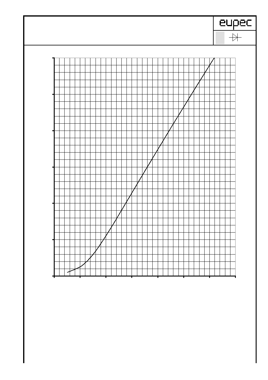
Grenzdurchlaþkennlinie / Limiting 0n-state characteristic i
F
=f(v
F
)
T
vj
= T
vj max
0
500
1.000
1.500
2.000
2.500
3.000
0,5
1
1,5
2
2,5
3
3,5
4
v
F
[V]
i
F
[A]