 | –≠–ª–µ–∫—Ç—Ä–æ–Ω–Ω—ã–π –∫–æ–º–ø–æ–Ω–µ–Ω—Ç: DD171N | –°–∫–∞—á–∞—Ç—å:  PDF PDF  ZIP ZIP |
March 1998
Marketing Information
DD 171 N
AK K
A
DD... 3)
European Power-
Semiconductor and
Electronics Company
GmbH + Co. KG
13
17
80
23
94
23
max. 11
screwing depth
M6

eupec GmbH + Co KG, Max-Planck-Str. 5, D59581 Warstein, Telefon +49 (0)2902/ 764-0, Telefax /764-256
DD 171 N
Elektrische Eigenschaften
Electrical properties
Hˆchstzul‰ssige Werte
Maximum rated values
Periodische Spitzensperrspannung
repetitive peak reverse voltage
t
vj
= -40∞C... t
vj max
V
RRM
600 800 1200
1400 1600 1800
V
Stoþspitzensperrspannung
non-repetitive peak reverse voltage
t
vj
= +25∞C... t
vj max
V
RSM
700 900 1300
1500 1700 1900
V
Durchlaþstrom-Grenzeffektivwert
RMS forward current
I
FRMSM
270
A
Dauergrenzstrom
mean forward current
t
c
= 100 ∞C
I
FAVM
170
A
Stoþstrom-Grenzwert
surge forward current
t
vj
= 25∞C, t
p
= 10 ms
I
FSM
6,6
kA
t
vj
= t
vj max
, t
p
= 10 ms
5,6
kA
Grenzlastintegral
I
2
t-value
t
vj
= 25∞C, t
p
= 10 ms
I
2
t
218 . 10
3
A
2
s
t
vj
= t
vj max
, t
p
= 10 ms
157 . 10
3
A
2
s
Charakteristische Werte
Characteristic values
Durchlaþspannung
forward voltage
t
vj
= t
vj max
, i
F
= 500 A
v
F
max. 1,26
V
Schleusenspannung
threshold voltage
t
vj
= t
vj max
V
T(TO)
0,75
V
Ersatzwiderstand
forward slope resistance
t
vj
= t
vj max
r
T
0,8 m
Sperrstrom
reverse current
t
vj
= t
vj max
, v
R
= V
RRM
i
R
max. 20
mA
Isolations-Pr¸fspannung
insulation test voltage
RMS, f= 50 Hz, t = 1 min
V
ISOL
2,5
kV
Thermische Eigenschaften
Thermal properties
Innerer W‰rmewiderstand
thermal resistance, junction
pro Modul/per module,
=180∞ sin
R
thJC
max. 0,130 ∞C/W
to case
pro Zweig/per arm,
=180∞ sin
max. 0,260 ∞C/W
pro Modul/per module, DC
max. 0,126 ∞C/W
pro Zweig/per arm,DC
max. 0,252 ∞C/W
Ðbergangs-W‰rmewiderstand
thermal resistance, case to heatsink
pro Modul/per module
R
thCK
max. 0,03 ∞C/W
pro Zweig/per arm
max. 0,06 ∞C/W
Hˆchstzul.Sperrschichttemperatur
max. junction temperature
t
vj max
150
∞C
Betriebstemperatur
operating temperature
t
c op
-40...+150
∞C
Lagertemperatur
storage temperature
t
stg
-40...+150 ∞C
2)
Mechanische Eigenschaften
Mechanical properties
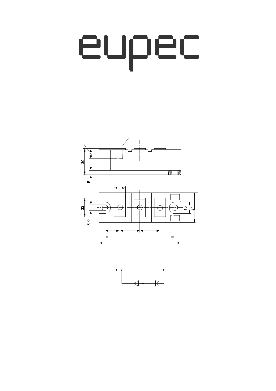
Geh‰use, siehe Seite
case, see page
1
Si-Element mit Druckkontakt
Si-pellet with pressure contact
Innere Isolation
internal insulation
AlN
Anzugsdrehmoment f¸r mechanische
Befestigung
mounting torque
Toleranz/tolerance +/- 15%
M1
6 Nm
Anzugsdrehmoment f¸r elektrische
Anschl¸sse
terminal connection torque
Toleranz/tolerance +5%/-10%
M2
6 Nm
Gewicht
weight
G
typ. 310
g
Kriechstrecke
creepage distance
15 mm
Schwingfestigkeit
vibration resistance
f = 50 Hz
50 m/s≤
2)
Gem‰þ DIN IEC 749 mit 747-1 gilt eine Zeitbegrenzung von 672 h. F¸r die im Betrieb auftretende Geh‰usetemperatur gilt keine zeitliche Begrenzung. /
According to DIN IEC 749 with 747-1 a time-limit of 672 h is defined. There is no time-limit set for case temperature during operation.

DD 171 N
Bild/Fig. 1
Durchlaþverlustleistung P
FAV
eines Zweiges
Forward power loss P
FAV
per arm
DD171N1
I
FAV
[A]
P
FAV
[W]
0
0
50
100
150
200
250
60∞
120∞
180∞
DC
300
50
100
150
200
250
300
180∞
H
=
Bild/Fig. 2
Hˆchstzul‰ssige Geh‰usetemperatur t
C
in Abh‰ngigkeit vom Zweigstrom
Maximum allowable case temperature t
C
versus current per arm
DC
t
C
[∞C]
I
FAVM
[A]
DD171N2
0
50
100
150
200
250
300
60∞
120∞
180∞
180∞
H
=
30
60
90
120
150
140
130
100
80
70
40
50
Bild/Fig. 5
Grenzstrom je Zweig I
F(OV)M
bei Luftselbstk¸hlung, t
A
=45∞C und verst‰rkter
Luftk¸hlung, t
A
=35∞C, Belastung nach Leerlauf, v
RM
= 0,8 V
RRM.
Limiting overload on-state current per arm I
F(OV)M
at natural (t
A
=45∞C) and
forced (t
A
=35∞) cooling, current surge under no-load conditions,
v
RM
= 0.8 V
RRM
.
DD171N5
2
4
t [ms]
I
F(OV)M
[kA]
10
1
10
2
10
3
6
8
2
4
6
8
1
2
3
4
t
A
= 35∞C
t
A
= 45∞C
5
0
6
Bild/Fig. 3
B2 - Zweipuls-Br¸ckenschaltung. Hˆchstzul‰ssiger Ausgangsstrom I
d
in Abh‰ngigkeit von der Umgebungstemperatur t
A
.
B2 - Two-pulse bridge circuit. Maximum allowable output current I
d
versus ambient temperature t
A
.
Parameter: W‰rmewiderstand zwischen Powerblock und Umgebung/
thermal resistance case to ambient R
thCA
DD171N3
20 40
60 80 100
P
tot
[W]
I
d
[A]
0
t
A
[∞C]
200
300
400
0
0,4
0,3
0,25
0,2
0,15
0,12
0,1
0,08
R
thCA
[∞C/W]
800
600
0,06 0,05
120
100
400
200
0,8
0,6
0,5
1,0
700
500
300
100
L-Last
R-Last
1,5
Bild/Fig. 4
B6 - Sechspuls-Br¸ckenschaltung. Hˆchstzul‰ssiger Ausgangsstrom I
d
in Abh‰ngigkeit von der Umgebungstemperatur t
A
.
B6 - Six-pulse bridge circuit. Maximum allowable output current I
d
versus ambient temperature t
A
.
Parameter: W‰rmewiderstand zwischen Powerblock und Umgebung/
thermal resistance case to ambient R
thCA
DD171N4
20 40
60 80 100
P
tot
[W]
I
d
[A]
0
t
A
[∞C]
200
300
500
400
0
0,4
0,3
0,25
0,2
0,15
0,12
0,1
0,08
R
thCA
[∞C/W]
800
600
1000
1200
0,06 0,05
120
100
400
200
0,8
0,6
0,5
1,0
DD171N08...16
1
10
100
Q
r
[µAs]
-di/dt [A/µs]
Bild/Fig. 6
Sperrverzˆgerungsladung / Recovered charge Q
r
= f(-di/dt)
t
vj
= t
vj max
, v
R
<= 0,5 V
RRM
, v
RM
= 0,8 V
RRM
Parameter: Durchlaþstrom / Forward current i
FM
i
FM
[ A ]
2000
2
4
7
20
40
70
200
400
700
100
4000
1000
1000
500
200
50
20
100

DD 171 N
Pos. n
1
2
3
4
5
6
7
R
thn
[∞C/W]
n
[s]
Analytische Elemente des transienten W‰rmewiderstandes Z
thJC
pro Zweig f¸r DC
Analytical elements of transient thermal impedance Z
thJC
per arm for DC
Analytische Funktion / Analytical function:
n
max
n=1
Z
thJC
= R
thn
(1-e )
t
-
n
Bild/Fig. 7
Transienter innerer W‰rmewiderstand je Zwieg Z
(th)JC
.
Transient thermal impedance, junction to case, per arm Z
(th)JC
.
t [s]
0,0094 0,0224 0,0586
0,162
0,0014 0,0253
0,267
1,68
DD171N7
Z
(th)JC
[∞C/W]
DC
60∞
0,12
0,16
0,24
0
120∞
180∞
180∞
0,04
0,08
10
-3
2 4 6 10
-2
2
4 6 10
-1
2
4 6 10
0
2
4 6 10
1
2
4 6 10
2
0,28
0,32