
I
C, nom
1200
A
I
C
1600
A
min.
typ.
max.
-
1,7
2,15
V
-
2
t.b.d.
V
vorl‰ufige Daten
preliminary data
gate emitter leakage current
Gate Emitter Reststrom
V
CE
= 0V, V
GE
= 20V, T
vj
= 25∞C
insulation test voltage
RMS, f= 50Hz, t= 1min.
collector emitter cut off current
Transistor Wechselrichter / transistor inverter
Gate Schwellenspannung
I
C
= 48mA, V
CE
= V
GE
, T
vj
= 25∞C,
reverse transfer capacitance
V
GE
= 0V, T
vj
= 25∞C, V
CE
= 1200V
gate charge
Kollektor Emitter Reststrom
kV
V
6,5
I≤t value
I≤t
V
GE(th)
gate threshold voltage
V
R
= 0V, t
p
= 10ms, T
vj
= 125∞C
Isolations Pr¸fspannung
Grenzlastintegral
2400
A
k A≤s
300
P
tot
A
DC forward current
+/- 20
5
V
GES
kW
V
gate emitter peak voltage
T
c
= 25∞C; Transistor
repetitive peak collector current
t
p
= 1ms, T
c
= 80∞C
Periodischer Kollektor Spitzenstrom
Dauergleichstrom
I
F
1200
5
5,8
2,5
V
ISOL
I
CES
repetitive peak forward current
t
p
= 1ms
I
FRM
Kollektor Dauergleichstrom
collector emitter voltage
Elektrische Eigenschaften / electrical properties
T
c
= 25∞C
DC collector current
T
vj
= 25∞C
Periodischer Spitzenstrom
Gesamt Verlustleistung
total power dissipation
Gate Emitter Spitzenspannung
V
CEsat
Charakteristische Werte / characteristic values
approved: SM TM; Christoph L¸bke
date of publication: 2002-07-30
Kollektor Emitter S‰ttigungsspannung
I
C
= 1200A, V
GE
= 15V, T
vj
= 25∞C,
collector emitter satration voltage
I
C
= 1200A, V
GE
= 15V, T
vj
= 125∞C,
2400
Technische Information / technical information
FF1200R12KE3
IGBT-Module
IGBT-Modules
Hˆchstzul‰ssige Werte / maximum rated values
Kollektor Emitter Sperrspannung
T
c
= 70∞C
revision: 2.0
prepared by: MOD-D2; Mark M¸nzer
V
CES
A
I
CRM
nF
-
4
R¸ckwirkungskapazit‰t
f= 1MHz, T
vj
= 25∞C, V
CE
= 25V, V
GE
= 0V
1200
V
Q
G
Eingangskapazit‰t
input capacitance
f= 1MHz, T
vj
= 25∞C, V
CE
= 25V, V
GE
= 0V
C
ies
Gateladung
V
GE
= -15V...+15V; V
CE=
...V
mA
-
-
-
C
res
11,5
-
86
I
GES
µC
-
-
400
nF
-
nA
5
-
-
1 (8)
DB_FF1200R12KE3_2.0.xls
2002-07-30

vorl‰ufige Daten
preliminary data
Technische Information / technical information
FF1200R12KE3
IGBT-Module
IGBT-Modules
min.
typ.
max.
-
0,60
-
µs
-
0,66
-
µs
-
0,23
-
µs
-
0,22
-
µs
-
0,82
-
µs
-
0,96
-
µs
-
0,15
-
µs
-
0,18
-
µs
-
2,2
2,8
V
-
2
-
V
-
340
-
A
-
530
-
A
-
57
-
µC
-
135
-
µC
-
18
-
mJ
-
35
-
mJ
A
-
m
W
-
Fallzeit (induktive Last)
fall time (inductive load)
I
C
= 1200A, V
CC
= 600V, L
s
= 60nH
V
GE
=±15V, R
Gon
=2,4
W, T
vj
= 125∞C
I
C
= 1200A, V
CC
= 600V, L
s
= 60nH
I
SC
-
4800
-
Einschaltverlustenergie pro Puls
turn on energy loss per pulse
Ausschaltverlustenergie pro Puls
245
-
190
stray inductance module
Modulindiktivit‰t
turn off energy loss per pulse
SC data
Kurzschlussverhalten
t
P
£ 10µs, V
GE
£ 15V, T
Vj
£ 125∞C
V
GE
=±15V, R
Goff
=0,62
W, T
vj
= 125∞C
Leitungswiderstand, Anschluss-Chip
lead resistance, terminal-chip
Charakteristische Werte / characteristic values
Diode Wechselrichter / diode inverter
T
c
= 25∞C
Q
r
Ausschaltenergie pro Puls
reverse recovery energy
E
rec
V
R
= 600V, V
GE
= -15V, T
vj
= 25∞C
V
R
= 600V, V
GE
= -15V, T
vj
= 125∞C
I
F
=I
C,nom
, -di
F
/dt= 5400A/µs
Sperrverzˆgerungsladung
recoverred charge
I
F
=I
C,nom
, -di
F
/dt= 5400A/µs
mJ
0,18
nH
L
sCE
-
20
-
E
off
-
R
CC¥/EE¥
Charakteristische Werte / characteristic values
V
GE
=±15V, R
Gon
=2,4
W, T
vj
= 125∞C
t
d,on
I
C
= 1200A, V
CC
= 600V
t
r
V
GE
=±15V, R
Gon
=2,4
W, T
vj
= 125∞C
I
C
= 1200A, V
CC
= 600V
V
GE
=±15V, R
Gon
=2,4
W, T
vj
=25∞C
V
GE
=±15V, R
Goff
=0,62
W, T
vj
=25∞C
V
GE
=±15V, R
Goff
=0,62
W,T
vj
= 125∞C
I
C
= 1200A, V
CC
= 600V
t
d,off
t
f
V
GE
=±15V, R
Goff
=0,62
W, T
vj
=25∞C
V
GE
=±15V, R
Goff
=0,62
W,T
vj
= 125∞C
I
RM
I
F
=I
C,nom
, -di
F
/dt= 5400A/µs
V
R
= 600V, V
GE
= -15V, T
vj
= 25∞C
-
E
on
V
CC
= 900V, V
CEmax
= V
CES
- L
sCE
∑
Ádi/dtÁ
V
F
Durchlassspannung
forward voltage
V
R
= 600V, V
GE
= -15V, T
vj
= 125∞C
I
F
= I
C, nom
, V
GE
= 0V, T
vj
= 25∞C
I
F
= I
C, nom
, V
GE
= 0V, T
vj
= 125∞C
R¸ckstromspitze
peak reverse recovery current
V
R
= 600V, V
GE
= -15V, T
vj
= 25∞C
V
R
= 600V, V
GE
= -15V, T
vj
= 125∞C
Anstiegszeit (induktive Last)
rise time (inductive load)
V
GE
=±15V, R
Gon
=2,4
W, T
vj
=25∞C
Einschaltverzˆgerungszeit (ind. Last)
turn on delay time (inductive load)
Abschaltverzˆgerungszeit (ind. Last)
turn off delay time (inductive load)
I
C
= 1200A, V
CC
= 600V
Transistor Wechselrichter / transistor inverter
mJ
-
2 (8)
DB_FF1200R12KE3_2.0.xls
2002-07-30

vorl‰ufige Daten
preliminary data
Technische Information / technical information
FF1200R12KE3
IGBT-Module
IGBT-Modules
min.
typ.
max.
R
thJC
-
-
0,013
K/W
-
-
0,025
K/W
-
-
0,021
K/W
-
-
0,042
K/W
-
0,006
-
K/W
-
0,012
-
K/W
10
mm
mm
-40
clearance
Luftstrecke
creepage distance
Kriechstrecke
T
vj op
terminal connection torque
M
pro Modul / per module
pro Zweig/ per arm;
l
Paste
/
l
grease
=1W/m*K
operation temperature
maximum junction temperature
Lagertemperatur
storage temperature
This technical information specifies semiconductor devices but promises no characteristics. It is valid
with the belonging technical notes.
Mechanische Eigenschaften / mechanical properties
Nm
Anzugsdrehmoment, mech. Befestigung
mounting torque
Nm
8
-
10
-
Mit dieser technischen Information werden Halbleiterbauelemente spezifiziert, jedoch keine
Eigenschaften zugesichert. Sie gilt in Verbindung mit den zugehˆrigen technischen Erl‰uterungen.
125
∞C
∞C
T
stg
-40
-
125
M
150
-
-
Thermische Eigenschaften / thermal properties
thermal resistance, case to heatsink
Hˆchstzul‰ssige Sperrschichttemp.
Betriebstemperatur
∞C
T
vj max
Gewicht
Al
2
O
3
weight
G
Anschl¸sse / terminal M4
Anschl¸sse / terminal M8
Anzugsdrehmoment, elektr. Anschl¸sse
M
4,25
Innere Isolation
comperative tracking index
Schraube / screw M5
case, see appendix
Geh‰use, siehe Anlage
internal insulation
CTI
>400
17
g
2,3
Nm
1500
-
5,75
1,7
-
R
thCK
Innerer W‰rmewiderstand
thermal resistance, junction to case
Transistor, DC, pro Modul / per module
Transistor, DC, pro Zweig / per arm
Diode/Diode, DC, pro Modul / per module
Diode/Diode, DC, pro Zweig / per arm
Ðbergangs W‰rmewiderstand
3 (8)
DB_FF1200R12KE3_2.0.xls
2002-07-30
vorl‰ufige Daten
preliminary data
Technische Information / technical information
FF1200R12KE3
IGBT-Module
IGBT-Modules
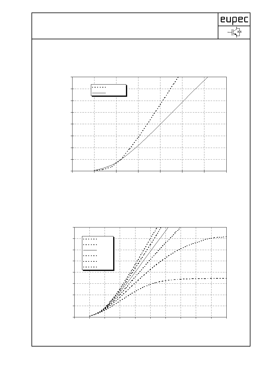
I
C
= f(V
CE
)
output characteristic (typical)
T
vj
= 125∞C
output characteristic (typical)
V
GE
= 15V
Ausgangskennlinienfeld (typisch)
I
C
= f(V
CE
)
Ausgangskennlinie (typisch)
0
300
600
900
1200
1500
1800
2100
2400
0,0
0,5
1,0
1,5
2,0
2,5
3,0
3,5
V
CE
[V]
I
C
[A
]
Tvj = 25∞C
Tvj = 125∞C
0
300
600
900
1200
1500
1800
2100
2400
0,0
0,5
1,0
1,5
2,0
2,5
3,0
3,5
4,0
4,5
5,0
V
CE
[V]
I
C
[A
]
Vge=19V
Vge=17V
Vge=15V
Vge=13V
Vge=11V
Vge=9V
4 (8)
DB_FF1200R12KE3_2.0.xls
2002-07-30
vorl‰ufige Daten
preliminary data
Technische Information / technical information
FF1200R12KE3
IGBT-Module
IGBT-Modules
transfer characteristic (typical)
I
C
= f(V
GE
)
V
CE
= 20V
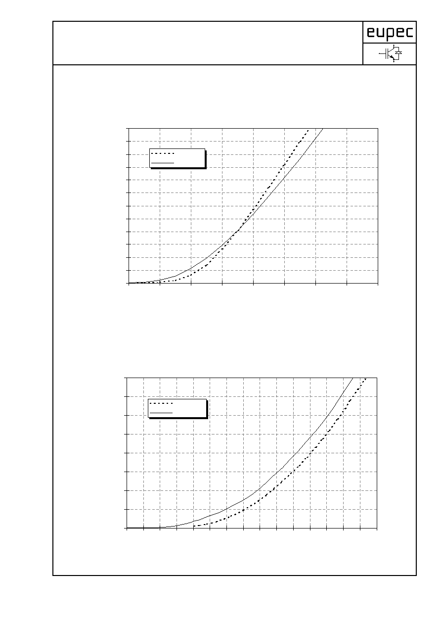
Durchlasskennlinie der Inversdiode (typisch)
I
F
= f(V
F
)
Ðbertragungscharakteristik (typisch)
forward caracteristic of inverse diode (typical)
0
200
400
600
800
1000
1200
1400
1600
1800
2000
2200
2400
5
6
7
8
9
10
11
12
13
V
GE
[V]
I
C
[A
]
Tvj=25∞C
Tvj=125∞C
0
300
600
900
1200
1500
1800
2100
2400
0,0 0,2 0,4 0,6 0,8 1,0 1,2 1,4 1,6 1,8 2,0 2,2 2,4 2,6 2,8 3,0
V
F
[V]
I
F
[A
]
Tvj = 25∞C
Tvj = 125∞C
5 (8)
DB_FF1200R12KE3_2.0.xls
2002-07-30