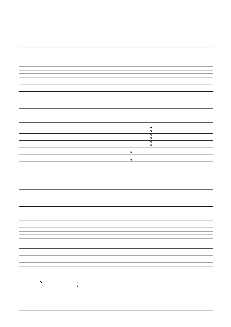
FF 400 R 12 KF 4
Hˆchstzul‰ssige Werte / Maximum rated values
Elektrische Eigenschaften / Electrical properties
Kollektor-Emitter-Sperrspannung
collector-emitter voltage
V
CES
1200 V
Kollektor-Dauergleichstrom
DC-collector current
I
C
400 A
Periodischer Kollektor Spitzenstrom
repetitive peak collctor current
t
p
=1 ms
I
CRM
800 A
Gesamt-Verlustleistung
total power dissipation
t
C
=25∞C, Transistor /transistor
P
tot
2700 W
Gate-Emitter-Spitzenspannung
gate-emitter peak voltage
V
GE
± 20 V
Dauergleichstrom
DC forward current
I
F
400 A
Periodischer Spitzenstrom
repetitive peak forw. current
t
p
=1ms
I
FRM
800 A
Isolations-Pr¸fspannung
insulation test voltage
RMS, f=50 Hz, t= 1 min.
V
ISOL
2,5 kV
Charakteristische Werte / Characteristic values: Transistor
min.
typ.
max.
Kollektor-Emitter S‰ttigungsspannung
collector-emitter saturation voltage
i
C
=400A, v
GE
=15V, t
vj
=25∞C
v
CE sat
-
2,7
3,2 V
i
C
=400A, v
GE
=15V, t
vj
=125∞C
-
3,3
3,9 V
Gate-Schwellenspannung
gate threshold voltage
i
C
=16mA, v
CE
=v
GE
, t
vj
=25∞C
v
GE(th)
4,5
5,5
6,5 V
Eingangskapazit‰t
input capacity
f
O
=1MHz,t
vj
=25∞C,v
CE
=25V, v
GE
=0V
C
ies
-
28
- nF
Kollektor-Emitter Reststrom
collector-emitter cut-off current
v
CE
=1200V, v
GE
=0V, t
vj
=25∞C
i
CES
-
8
- mA
v
CE
=1200V, v
GE
=0V, t
vj
=125∞C
-
32
- mA
Gate-Emitter Reststrom
gate leakage current
v
CE
=0V, v
GE
=20V, t
vj
=25∞C
i
GES
-
-
400 nA
Emitter-Gate Reststrom
gate leakage current
v
CE
=0V, v
EG
=20V, t
vj
=25∞C
i
EGS
-
-
400 nA
Einschaltzeit (induktive Last)
turn-on time (inductive load)
i
C
=400A,v
CE
=600V,v
L
=±15V,R
G
=3,6 ,t
vj
= 25∞C t
on
-
0,7
- µs
i
C
=400A,v
CE
=600V,v
L
=±15V,R
G
=3,6 ,t
vj
=125∞C
-
0,8
- µs
Speicherzeit (induktive Last)
storage time (inductive load)
i
C
=400A,v
CE
=600V,v
L
=±15V,R
G
=3,6 ,t
vj
= 25∞C t
s
-
0,9
- µs
i
C
=400A,v
CE
=600V,v
L
=±15V,R
G
=3,6 ,t
vj
=125∞C
-
1,0
- µs
Fallzeit (induktive Last)
fall time (inductive load)
i
C
=400A,v
CE
=600V,v
L
=±15V,R
G
=3,6 ,t
vj
= 25∞C t
f
-
0,10
- µs
i
C
=400A,v
CE
=600V,v
L
=±15V,R
G
=3,6 ,t
vj
=125∞C
-
0,15
- µs
Einschaltverlustenergie pro puls
turn-on energie per pulse
i
C
=400A, v
CE
=600V, L
s
=70nH
E
on
v
L
=±15V, R
G
=3,6 , t
vj
=125∞C
-
70
- mWs
Abschaltverlustenergie pro Puls
turn-off energie loss per pulse
i
C
=400A, v
CE
=600V, L
s
=70nH
E
off
v
L
=±15V, R
G
=3,6 , t
vj
=125∞C
-
60
- mWs
Charakteristische Werte / Characteristic values
Inversdiode / Inverse diode
Durchlaþspannung
forward voltage
i
F
=400A, v
GE
=0V, t
vj
=25∞C
v
F
-
2,2
2,7 V
i
F
=400A, v
GE
=0V, t
vj
=125∞C
-
2,0
2,5 V
R¸ckstromspitze
peak reverse recovery current
i
F
=400A, v
RM
=600V, v
EG
= 10V
I
RM
-di
F
/dt = 2,0 kA/µs, t
vj
= 25∞C
-
140
- A
-di
F
/dt = 2,0 kA/µs, t
vj
= 125∞C
-
240
- A
Sperrverzˆgerungsladung
recovered charge
i
F
=400A, v
RM
=600V, v
EG
= 10V
Q
r
-di
F
/dt = 3,0 kA/µs, t
vj
= 25∞C
-
18
- µAs
-di
F
/dt = 3,0 kA/µs, t
vj
= 125∞C
-
50
- µAs
Thermische Eigenschaften / Thermal properties
Innerer W‰rmewiderstand
thermal resistance, junction to case Transistor / transistor, DC
R
thJC
0,023 ∞C/W
Transistor,DC,pro Zweig/per arm
0,046 ∞C/W
Diode, DC, pro Modul/per module
0,044 ∞C/W
Diode, DC, pro Zweig/per arm
0,088 ∞C/W
Ðbergangs-W‰rmewiderstand
thermal resistance, case to heatsink pro Modul / per Module
R
thCK
0,01 ∞C/W
pro Zweig / per arm
0,02 ∞C/W
Hˆchstzul. Sperrschichttemperatur
max. junction temperature
pro Modul / per Module
t
vj max
150 ∞C
Betriebstemperatur
operating temperature
Transistor / transistor
t
c op
-40...+150 ∞C
Lagertemperatur
storage temperature
t
stg
-40...+125 ∞C
Mechanische Eigenschaften / Mechanical properties
Geh‰use, siehe Anlage
case, see appendix
Seite / page
1
Innere Isolation
internal insulation
AI
2
O
3
Anzugsdrehmoment f. mech. Befestigung
mounting torque
terminals M6 /
tolerance +/-15%
M1
5 Nm
Anzugsdrehmoment f. elektr. Anschl¸sse
terminal connection torque
terminals M4 /
tolerance +/-15%
M2
2 Nm
terminals M8
8...10 Nm
Gewicht
weight
G
ca. 1500 g
Bedingung f¸r den Kurzschluþschutz / Conditions for short-circuit protection
t
fg
= 10 µs
V
CC
= 750 V
v
L
= ±15 V
v
CEM
= 900 V
R
GF
= R
GR
= 3,6
i
CMK1
3500 A
t
vj
= 125∞C
i
CMK2
3000 A
Unabh‰ngig davon gilt bei abweichenden Bedingungen / with regard to other conditions
CEM
= V
CES
- 20nH x |di
c
/dt|
Mit dieser technischen Information werden Halbleiterbauelemente spezifiziert, jedoch keine Eigenschaften zugesichert. Sie gilt in Verbindung mit den
zugehˆrigen Technischen Erl‰uterungen. This technical information specifies semiconductor devices but promises no characteristics. It is valid in
combination with the belonging technical notes.
v