
Technische Information / Technical Information
IGBT-Module
IGBT-Modules
FF 400 R 33 KF2
Datenblatt
data sheet
Hˆchstzul‰ssige Werte / Maximum rated values
Elektrische Eigenschaften / Electrical properties
Kollektor-Emitter-Sperrspannung
T
j
= 25∞C
V
CES
3300
V
collector-emitter voltage
T
j
= -25∞C
3300
Kollektor-Dauergleichstrom
T
C
= 80∞C
I
C,nom.
400
A
DC-collector current
T
C
= 25 ∞C
I
C
660
A
Periodischer Kollektor Spitzenstrom
repetitive peak collector current
t
P
= 1 ms, T
C
= 80∞C
I
CRM
800
A
Gesamt-Verlustleistung
total power dissipation
T
C
=25∞C, Transistor
P
tot
4,8
kW
Gate-Emitter-Spitzenspannung
gate-emitter peak voltage
V
GES
+/- 20V
V
Dauergleichstrom
DC forward current
I
F
400
A
Periodischer Spitzenstrom
repetitive peak forw. current
t
P
= 1 ms
I
FRM
800
A
Grenzlastintegral der Diode
I
2
t - value, Diode
V
R
= 0V, t
p
= 10ms, T
Vj
= 125∞C
I
2
t
A
2
s
Spitzenverlustleistung der Diode
maximum power dissipation diode
T
j
= 125∞C
P
RQM
400
kW
Isolations-Pr¸fspannung
insulation test voltage
RMS, f = 50 Hz, t = 1 min.
V
ISOL
6.000
V
Teilentladungs-Aussetzspannung
partial discharge extinction voltage
RMS, f = 50 Hz, Q
PD
10 pC (acc. to IEC 1287)
V
ISOL
2.600
V
Charakteristische Werte / Characteristic values
Transistor / Transistor
min.
typ.
max.
Kollektor-Emitter S‰ttigungsspannung
I
C
= 400A, V
GE
= 15V, Tvj = 25∞C
V
CE sat
-
3,40
4,25
V
collector-emitter saturation voltage
I
C
= 400A, V
GE
= 15V, T
vj
= 125∞C
-
4,30
5,00
V
Gate-Schwellenspannung
gate threshold voltage
I
C
= 40 mA, V
CE
= V
GE
, T
vj
= 25∞C
V
GE(th)
4,2
5,1
6,0
V
Eingangskapazit‰t
input capacitance
f = 1MHz,T
vj
= 25∞C,V
CE
= 25V, V
GE
= 0V
C
ies
-
50
-
nF
R¸ckwirkungskapazit‰t
reverse transfer capacitance
f = 1MHz,T
vj
= 25∞C,V
CE
= 25V, V
GE
= 0V
C
res
-
2,7
-
nF
Gateladung
gate charge
V
GE
= -15V ... + 15V, V
CE
= 1800V
Q
G
-
8
-
µC
Kollektor-Emitter Reststrom
V
CE
= 3300V, V
GE
= 0V, T
vj
= 25∞C
I
CES
-
0,05
4
mA
collector-emitter cut-off current
V
CE
= 3300V, V
GE
= 0V, T
vj
= 125∞C
-
20
50
mA
Gate-Emitter Reststrom
gate-emitter leakage current
V
CE
= 0V, V
GE
= 20V, T
vj
= 25∞C
I
GES
-
-
400
nA
prepared by: J¸rgen Gˆttert
date of publication : 08.06.99
approved by: Chr. L¸bke; 20.07.99
revision: 2
55.600
1 (9)
Datenblatt FF 400 R 33 KF2
20.07.99
Technische Information / Technical Information
IGBT-Module
IGBT-Modules
FF 400 R 33 KF2
Datenblatt
data sheet
Charakteristische Werte / Characteristic values
Transistor / Transistor
min.
typ.
max.
Einschaltverzˆgerungszeit (ind. Last)
I
C
= 400 A, V
CC
= 1800V
turn on delay time (inductive load)
V
GE
= ±15V, R
G
= 3,6
, C
GE
= 68nF, T
vj
= 25∞C
t
d,on
-
370
-
ns
V
GE
= ±15V, R
G
= 3,6
, C
GE
= 68nF, T
vj
= 125∞C
-
350
-
ns
Anstiegszeit (induktive Last)
I
C
= 400 A, V
CC
= 1800V
rise time (inductive load)
V
GE
= ±15V, R
G
= 3,6
, C
GE
= 68nF, T
vj
= 25∞C
t
r
-
250
-
ns
V
GE
= ±15V, R
G
= 3,6
, C
GE
= 68nF, T
vj
= 125∞C
-
270
-
ns
Abschaltverzˆgerungszeit (ind. Last)
I
C
= 400 A, V
CC
= 1800V
turn off delay time (inductive load)
V
GE
= ±15V, R
G
= 3,6
, C
GE
= 68nF, T
vj
= 25∞C
t
d,off
-
1550
-
ns
V
GE
= ±15V, R
G
= 3,6
, C
GE
= 68nF, T
vj
= 125∞C
-
1700
-
ns
Fallzeit (induktive Last)
I
C
= 400 A, V
CC
= 1800V
fall time (inductive load)
V
GE
= ±15V, R
G
= 3,6
, C
GE
= 68nF, T
vj
= 25∞C
t
f
-
200
-
ns
V
GE
= ±15V, R
G
= 3,6
, C
GE
= 68nF, T
vj
= 125∞C
-
200
-
ns
Einschaltverlustenergie pro Puls
I
C
= 400 A, V
CC
= 1800V, V
GE
= 15V
turn-on energy loss per pulse
R
G
= 3,6
, C
GE
= 68 nF, T
vj
= 125∞C, L
S
= 60nH
E
on
-
960
-
mWs
Abschaltverlustenergie pro Puls
I
C
= 400 A, V
CC
= 1800V, V
GE
= 15V
turn-off energy loss per pulse
R
G
= 3,6
, C
GE
= 68 nF, T
vj
= 125∞C, L
S
= 60nH
E
off
-
510
-
mWs
Kurzschluþverhalten
t
P
10µsec, V
GE
15V
SC Data
T
Vj
125∞C, V
CC
=2500V, V
CEmax
=V
CES
-L
sCE
∑dI/dt
I
SC
-
2000
-
A
Modulinduktivit‰t
stray inductance module
L
sCE
-
25
-
nH
Modul-Leitungswiderstand, Anschl¸sse - Chip
lead resistance, terminals - chip
T = 25∞C
R
CC'+EE'
-
0,37
-
m
Charakteristische Werte / Characteristic values
Diode / Diode
min.
typ.
max.
Durchlaþspannung
I
F
= 400 A, V
GE
= 0V, T
vj
= 25∞C
V
F
-
2,80
3,50
V
forward voltage
I
F
= 400 A, V
GE
= 0V, T
vj
= 125∞C
-
2,80
3,50
V
R¸ckstromspitze
I
F
= 400 A, - di
F
/dt = 1200 A/µsec
peak reverse recovery current
V
R
= 1800V, VGE = -10V, T
vj
= 25∞C
I
RM
-
330
-
A
V
R
= 1800V, VGE = -10V, T
vj
= 125∞C
-
350
-
A
Sperrverzˆgerungsladung
I
F
= 400 A, - di
F
/dt = 1200 A/µsec
recovered charge
V
R
= 1800V, VGE = -10V, T
vj
= 25∞C
Q
r
-
235
-
µAs
V
R
= 1800V, VGE = -10V, T
vj
= 125∞C
-
440
-
µAs
Abschaltenergie pro Puls
I
F
= 400 A, - di
F
/dt = 1200 A/µsec
reverse recovery energy
V
R
= 1800V, VGE = -10V, T
vj
= 25∞C
E
rec
-
245
-
mWs
V
R
= 1800V, VGE = -10V, T
vj
= 125∞C
-
500
-
mWs
2 (9)
Datenblatt FF 400 R 33 KF2
20.07.99
Technische Information / Technical Information
IGBT-Module
IGBT-Modules
FF 400 R 33 KF2
Datenblatt
data sheet
Thermische Eigenschaften / Thermal properties
min.
typ.
max.
Innerer W‰rmewiderstand
Transistor / transistor, DC
R
thJC
-
-
0,026
K/W
thermal resistance, junction to case
Diode/Diode, DC
-
-
0,051
K/W
Ðbergangs-W‰rmewiderstand
thermal resistance, case to heatsink
pro Modul / per module
Paste
= 1 W/m*K /
grease
= 1 W/m*K
R
thCK
-
0,006
-
K/W
Hˆchstzul‰ssige Sperrschichttemperatur
maximum junction temperature
T
vj
-
-
150
∞C
Betriebstemperatur
operation temperature
T
op
-40
-
125
∞C
Lagertemperatur
storage temperature
T
stg
-40
-
125
∞C
Mechanische Eigenschaften / Mechanical properties
Geh‰use, siehe Anlage
case, see appendix
Material Modulgrundplatte
material of module baseplate
AlSiC
Innere Isolation
internal insulation
AlN
Kriechstrecke
creepage distance
32,2
mm
Luftstrecke
clearance
19,1
mm
CTI
comperative tracking index
> 400
Anzugsdrehmoment f. mech. Befestigung
M1
5
Nm
mounting torque
Anzugsdrehmoment f. elektr. Anschl¸sse
terminals M4
M2
2
Nm
terminal connection torque
terminals M8
8 .. 10
Nm
Gewicht
weight
G
1100
g
Mit dieser technischen Information werden Halbleiterbauelemente spezifiziert, jedoch keine Eigenschaften zugesichert.
Sie gilt in Verbindung mit den zugehˆrigen Technischen Erl‰uterungen.
This technical information specifies semiconductor devices but promises no characteristics. It is
valid in combination with the belonging technical notes.
3 (9)
Datenblatt FF 400 R 33 KF2
20.07.99
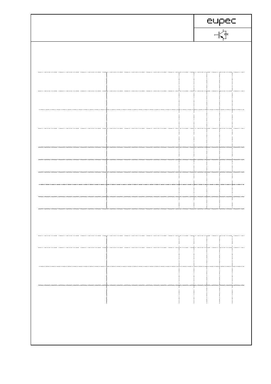
Technische Information / Technical Information
IGBT-Module
IGBT-Modules
FF 400 R 33 KF2
Datenblatt
data sheet
I
C
[A]
V
CE
[V]
I
C
[A]
V
CE
[V]
0
100
200
300
400
500
600
700
800
0,0
0,5
1,0
1,5
2,0
2,5
3,0
3,5
4,0
4,5
5,0
5,5
6,0
6,5
7,0
T = 25∞C
T = 125∞C
Ausgangskennlinie (typisch) I
C
= f (V
CE
)
Output characteristic (typical)
V
GE
= 15V
0
100
200
300
400
500
600
700
800
0,0
0,5
1,0
1,5
2,0
2,5
3,0
3,5
4,0
4,5
5,0
5,5
6,0
6,5
7,0
VGE = 8V
VGE = 9V
VGE = 10V
VGE = 12V
VGE = 15V
VGE = 20V
Ausgangskennlinienfeld (typisch) I
C
= f (V
CE
)
Output characteristic (typical)
T
vj
= 125∞C
4 (9)
Datenblatt FF 400 R 33 KF2
20.07.99

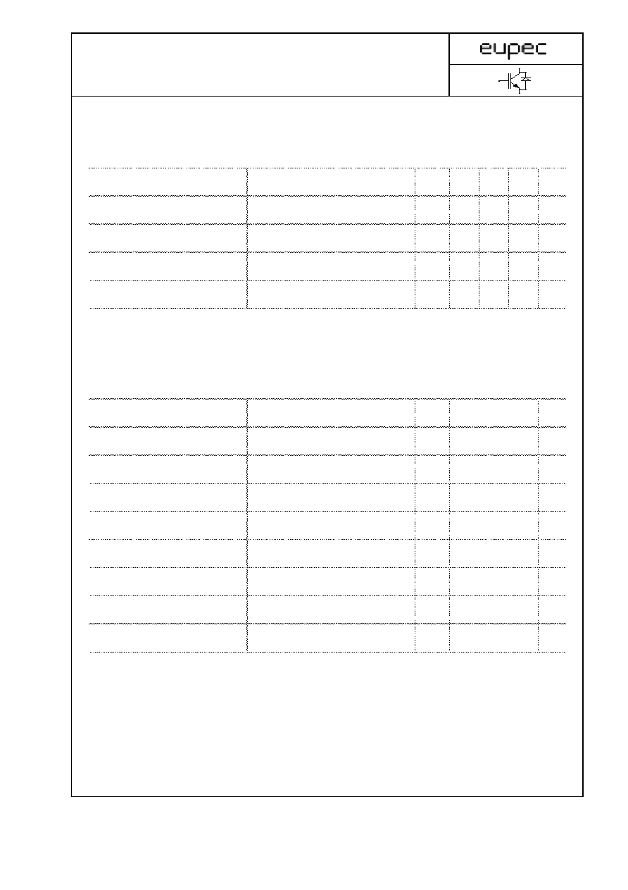
Technische Information / Technical Information
IGBT-Module
IGBT-Modules
FF 400 R 33 KF2
Datenblatt
data sheet
I
C
[A]
V
GE
[V]
I
F
[A]
V
F
[V]
0
100
200
300
400
500
600
700
800
5
6
7
8
9
10
11
12
13
T = 25∞C
T = 125∞C
Ðbertragungscharakteristik (typisch) I
C
= f (V
GE
)
Transfer characteristic (typical)
V
CE
= 20V
0
100
200
300
400
500
600
700
800
0,0
0,5
1,0
1,5
2,0
2,5
3,0
3,5
4,0
Tj = 25∞C
Tj = 125∞C
Durchlaþkennlinie der Inversdiode (typisch) I
F
= f (V
F
)
Forward characteristic of inverse diode (typical)
5 (9)
Datenblatt FF 400 R 33 KF2
20.07.99
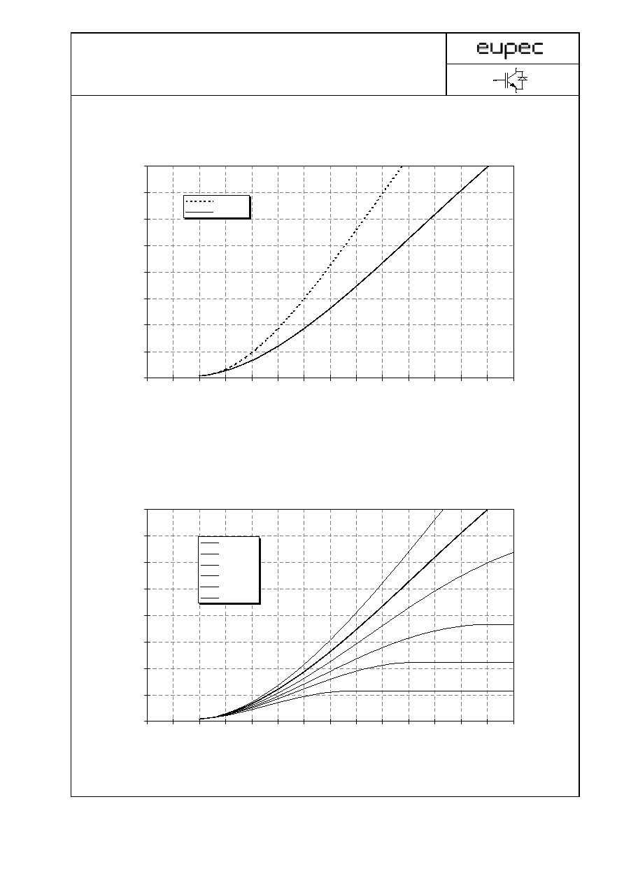
Technische Information / Technical Information
IGBT-Module
IGBT-Modules
FF 400 R 33 KF2
Datenblatt
data sheet
E [
m
J]
I
C
[A]
E [
m
J]
R
G
[
]
0
500
1000
1500
2000
2500
3000
3500
0
100
200
300
400
500
600
700
800
Eon
Eoff
Erec
Schaltverluste (typisch) E
on
= f (I
C
) , E
off
= f (I
C
) , E
rec
= f (I
C
)
Switching losses (typical)
R
G,on
= 3,6
,
R
G,off
= 3,6
, C
GE
= 68 nF, V
CE
= 1800V, T
j
=
125∞C
0
500
1000
1500
2000
2500
3000
3500
4000
0
5
10
15
20
25
30
35
40
45
Eon
Eoff
Erec
Schaltverluste (typisch) E
on
= f (R
G
) , E
off
= f (R
G
) , E
rec
= f (R
G
)
Switching losses (typical)
I
C
= 400 A , C
GE
= 68 nF, V
CE
= 1800V , T
j
= 125∞C
6 (9)
Datenblatt FF 400 R 33 KF2
20.07.99
Technische Information / Technical Information
IGBT-Module
IGBT-Modules
FF 400 R 33 KF2
Datenblatt
data sheet
I
C
[A
]
V
CE
[V]
I
R
[A
]
V
R
[V]
0
100
200
300
400
500
600
700
800
900
0
500
1000
1500
2000
2500
3000
3500
IC,Modul
IC,Chip
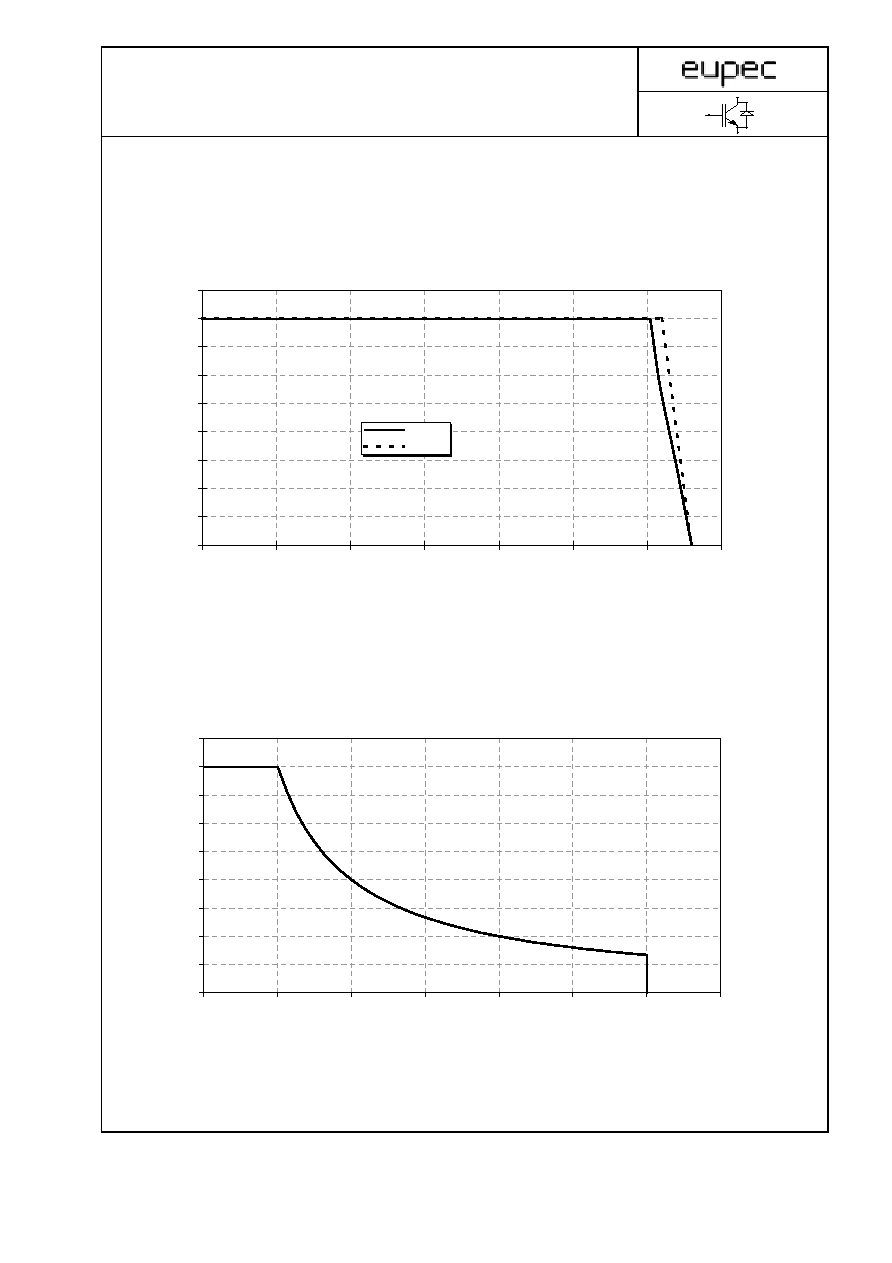
Sicherer Arbeitsbereich IGBT (RBSOA)
R
G,off
= 3,6
, C
GE
= 68 nF
Reverse bias safe operation area IGBT (RBSOA)
T
vj
= 125∞C
0
100
200
300
400
500
600
700
800
900
0
500
1000
1500
2000
2500
3000
3500
Sicherer Arbeitsbereich Diode (SOA)
T
vj
= 125∞C
safe operation area Diode (SOA)
7 (9)
Datenblatt FF 400 R 33 KF2
20.07.99
Technische Information / Technical Information
IGBT-Module
IGBT-Modules
FF 400 R 33 KF2
Datenblatt
data sheet
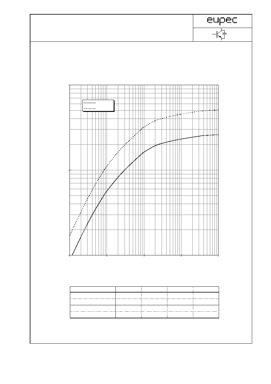
Z
th
J
C
[K
/ W]
t [sec]
i
1
2
3
4
r
i
[K/kW]
: IGBT
4,76
12,98
3,86
4,40
i
[sec]
: IGBT
0,0068
0,0642
0,3209
2,0212
r
i
[K/kW]
: Diode
9,34
25,47
7,57
8,63
i
[sec]
: Diode
0,0068
0,0642
0,3209
2,0212
Transienter W‰rmewiderstand Z
thJC
= f (t)
Transient thermal impedance
0,001
0,01
0,1
0,001
0,01
0,1
1
10
Zth:IGBT
Zth:Diode
8 (9)
Datenblatt FF 400 R 33 KF2
20.07.99

Technische Information / Technical Information
IGBT-Module
IGBT-Modules
FF 400 R 33 KF2
Datenblatt
data sheet
Geh‰usemaþe / Schaltbild
Package outline / Circuit diagram
9 (9)
Datenblatt FF 400 R 33 KF2
20.07.99