Technische Information / Technical Information
IGBT-Module
IGBT-Modules
FF 401 R 17 KF6C B2
vorlšufige Daten
preliminary data
HŲchstzulšssige Werte / Maximum rated values
Elektrische Eigenschaften / Electrical properties
Kollektor-Emitter-Sperrspannung
collector-emitter voltage
T
vj
= 25įC
V
CES
1700
V
Kollektor-Dauergleichstrom
T
C
= 80 įC
I
C,nom.
400
A
DC-collector current
T
C
= 25 įC
I
C
650
A
Periodischer Kollektor Spitzenstrom
repetitive peak collector current
t
P
= 1 ms, T
C
= 80įC
I
CRM
800
A
Gesamt-Verlustleistung
total power dissipation
T
C
=25įC, Transistor
P
tot
3,1
kW
Gate-Emitter-Spitzenspannung
gate-emitter peak voltage
V
GES
+/- 20V
V
Dauergleichstrom
DC forward current
I
F
400
A
Periodischer Spitzenstrom
repetitive peak forw. current
t
P
= 1 ms
I
FRM
800
A
Grenzlastintegral der Diode
I
2
t - value, Diode
V
R
= 0V, t
p
= 10ms, T
Vj
= 125įC
I
2
t
45
kA
2
s
Isolations-PrŁfspannung
insulation test voltage
RMS, f = 50 Hz, t = 1 min.
V
ISOL
4
kV
Charakteristische Werte / Characteristic values
Transistor / Transistor
min.
typ.
max.
Kollektor-Emitter Sšttigungsspannung
I
C
= 400A, V
GE
= 15V, T
vj
= 25įC
V
CE sat
-
2,6
3,1
V
collector-emitter saturation voltage
I
C
= 400A, V
GE
= 15V, T
vj
= 125įC
-
3,1
3,6
V
Gate-Schwellenspannung
gate threshold voltage
I
C
= 30mA , V
CE
= V
GE
, T
vj
= 25įC
V
GE(th)
4,5
5,5
6,5
V
Gateladung
gate charge
V
GE
= -15V ... +15V
Q
G
-
4,8
-
ĶC
Eingangskapazitšt
input capacitance
f = 1MHz,T
vj
= 25įC,V
CE
= 25V, V
GE
= 0V
C
ies
-
27
-
nF
RŁckwirkungskapazitšt
reverse transfer capacitance
f = 1MHz,T
vj
= 25įC,V
CE
= 25V, V
GE
= 0V
C
res
-
1,3
-
nF
Kollektor-Emitter Reststrom
V
CE
= 1700V, V
GE
= 0V, T
vj
= 25įC
I
CES
-
-
5
mA
collector-emitter cut-off current
Gate-Emitter Reststrom
gate-emitter leakage current
V
CE
= 0V, V
GE
= 20V, T
vj
= 25įC
I
GES
-
-
400
nA
prepared by: Alfons Wiesenthal
date of publication:28.03.2001
approved by: Christoph LŁbke; 12.04.2001
revision: 2 (preliminary)
1(8)
FF401R17KF6CB2_V.xls

Technische Information / Technical Information
IGBT-Module
IGBT-Modules
vorlšufige Daten
preliminary data
Charakteristische Werte / Characteristic values
Transistor / Transistor
min.
typ.
max.
EinschaltverzŲgerungszeit (ind. Last)
I
C
= 400A, V
CE
= 900V
turn on delay time (inductive load)
V
GE
= Ī15V, R
G
= 1,8
W
, T
vj
= 25įC
t
d,on
-
0,4
-
Ķs
V
GE
= Ī15V, R
G
=1,8
W
, T
vj
= 125įC
-
0,4
-
Ķs
Anstiegszeit (induktive Last)
I
C
= 400A, V
CE
= 900V
rise time (inductive load)
V
GE
= Ī15V, R
G
=1,8
W
, T
vj
= 25įC
t
r
-
0,15
-
Ķs
V
GE
= Ī15V, R
G
=1,8
W
, T
vj
= 125įC
-
0,15
-
Ķs
AbschaltverzŲgerungszeit (ind. Last)
I
C
= 400A, V
CE
= 900V
turn off delay time (inductive load)
V
GE
= Ī15V, R
G
= 3,6
W
, T
vj
= 25įC
t
d,off
-
1,1
-
Ķs
V
GE
= Ī15V, R
G
= 3,6
W
, T
vj
= 125įC
-
1,1
-
Ķs
Fallzeit (induktive Last)
I
C
= 400A, V
CE
= 900V
fall time (inductive load)
V
GE
= Ī15V, R
G
= 3,6
W
, T
vj
= 25įC
t
f
-
0,1
-
Ķs
V
GE
= Ī15V, R
G
= 3,6
W
, T
vj
= 125įC
-
0,11
-
Ķs
Einschaltverlustenergie pro Puls
I
C
= 400A, V
CE
= 900V, V
GE
= 15V
turn-on energy loss per pulse
R
G,on
= 1,8
W
, T
vj
= 125įC, L
S
= 60nH
E
on
-
190
-
mWs
Abschaltverlustenergie pro Puls
I
C
= 400A, V
CE
= 900V, V
GE
= 15V
turn-off energy loss per pulse
R
G
= 3,6
W
, T
vj
= 125įC, L
S
= 60nH
E
off
-
150
-
mWs
KurzschluŖverhalten
t
P
£
10Ķsec, V
GE
£
15V
SC Data
T
Vj
£
125įC, V
CC
=1000V, V
CEmax
=V
CES
-L
sCE
∑dI/dt
I
SC
-
1600
-
A
Modulinduktivitšt
stray inductance module
L
sCE
-
58
-
nH
Modulleitungswiderstand, AnschlŁsse - Chip
module lead resistance, terminals - chip
pro Zweig / per arm
R
CCī+EEī
-
0,78
-
m
W
Charakteristische Werte / Characteristic values
Diode / Diode
min.
typ.
max.
DurchlaŖspannung
I
F
= 400A, V
GE
= 0V, T
vj
= 25įC
V
F
-
2,1
2,5
V
forward voltage
I
F
= 400A, V
GE
= 0V, T
vj
= 125įC
-
2,1
2,5
V
RŁckstromspitze
I
F
= 400A, - di
F
/dt =2400 A/Ķsec
peak reverse recovery current
V
R
= 900V, VGE = -10V, T
vj
= 25įC
I
RM
-
270
-
A
V
R
= 900V, VGE = -10V, T
vj
= 125įC
-
320
-
A
SperrverzŲgerungsladung
I
F
= 400A, - di
F
/dt =2400 A/Ķsec
recovered charge
V
R
= 900V, VGE = -10V, T
vj
= 25įC
Q
r
-
75
-
ĶAs
V
R
= 900V, VGE = -10V, T
vj
= 125įC
-
145
-
ĶAs
Abschaltenergie pro Puls
I
F
= 400A, - di
F
/dt =2400 A/Ķsec
reverse recovery energy
V
R
= 900V, VGE = -10V, T
vj
= 25įC
E
rec
-
35
-
mWs
V
R
= 900V, VGE = -10V, T
vj
= 125įC
-
70
-
mWs
FF 401 R 17 KF6C B2
2(8)
FF401R17KF6CB2_V.xls
Technische Information / Technical Information
IGBT-Module
IGBT-Modules
FD 401 R 17 KF6C B2
vorlšufige Daten
preliminary data
Thermische Eigenschaften / Thermal properties
min.
typ.
max.
Innerer Wšrmewiderstand
Transistor / transistor, DC
R
thJC
-
-
0,04
K/W
thermal resistance, junction to case
Diode/Diode, DC
-
-
0,068
K/W
‹bergangs-Wšrmewiderstand
thermal resistance, case to heatsink
pro Zweig / per arm
pro Modul / per module
l
Paste
= 1 W/m*K /
l
grease
= 1 W/m*K
R
thCK
-
0,04
0,02
K/W
HŲchstzulšssige Sperrschichttemperatur
maximum junction temperature
T
vj
-
-
150
įC
Betriebstemperatur
operation temperature
T
vj op
-40
-
125
įC
Lagertemperatur
storage temperature
T
stg
-40
-
125
įC
Mechanische Eigenschaften / Mechanical properties
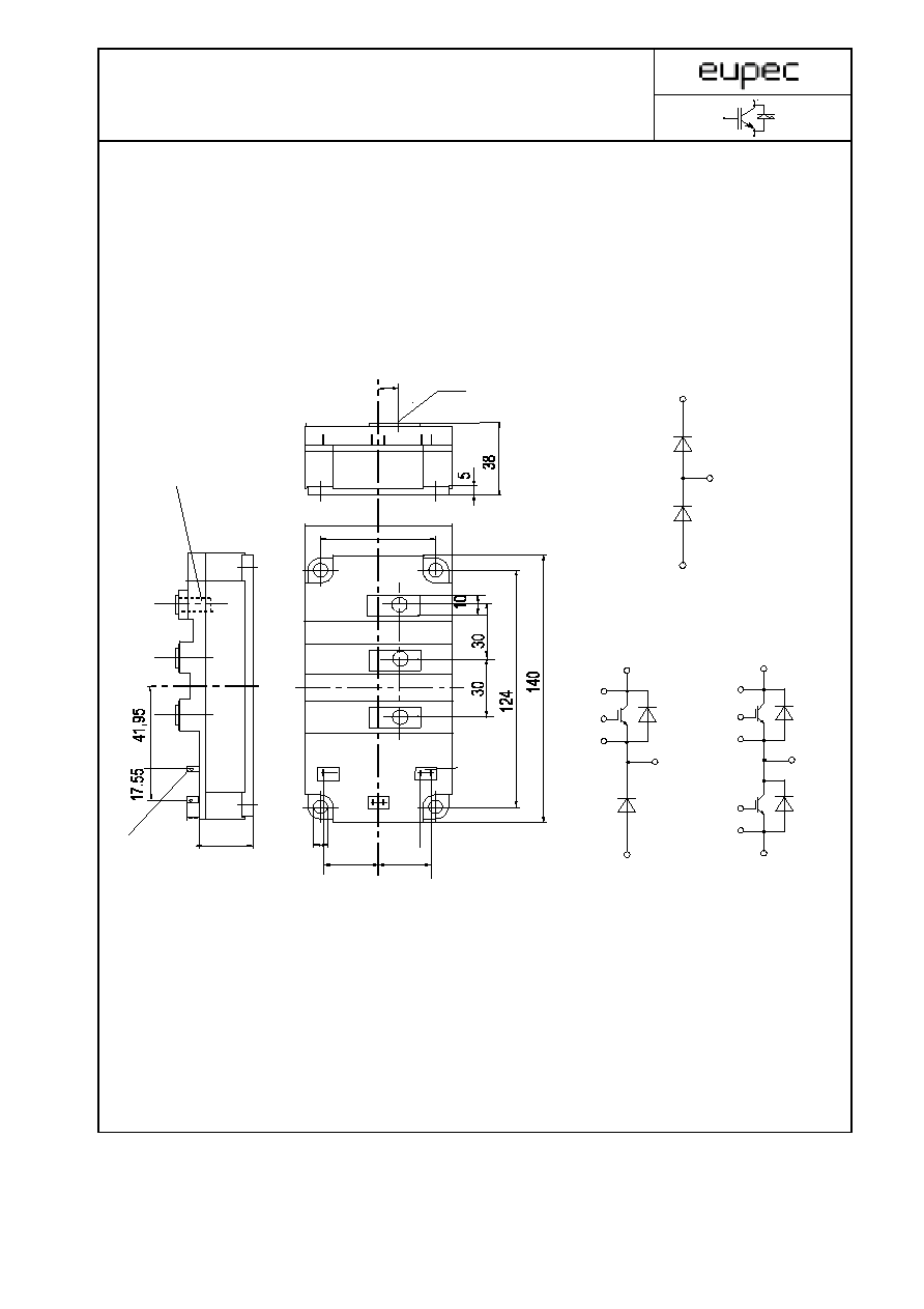
Gehšuse, siehe Anlage
case, see appendix
Innere Isolation
internal insulation
AlN
Kriechstrecke
creepage distance
32
mm
Luftstrecke
clearance
19
mm
CTI
comperative tracking index
>400
Anzugsdrehmoment f. mech. Befestigung
M1
5
Nm
mounting torque
Anzugsdrehmoment f. elektr. AnschlŁsse
terminals M5
M2
4
Nm
terminal connection torque
Nm
Gewicht
weight
G
500
g
Mit dieser technischen Information werden Halbleiterbauelemente spezifiziert, jedoch keine Eigenschaften zugesichert.
Sie gilt in Verbindung mit den zugehŲrigen Technischen Erlšuterungen.
This technical information specifies semiconductor devices but promises no characteristics. It is
valid in combination with the belonging technical notes.
3(8)
FD401R17KF6CB2_V.xls
Technische Information / Technical Information
IGBT-Module
IGBT-Modules
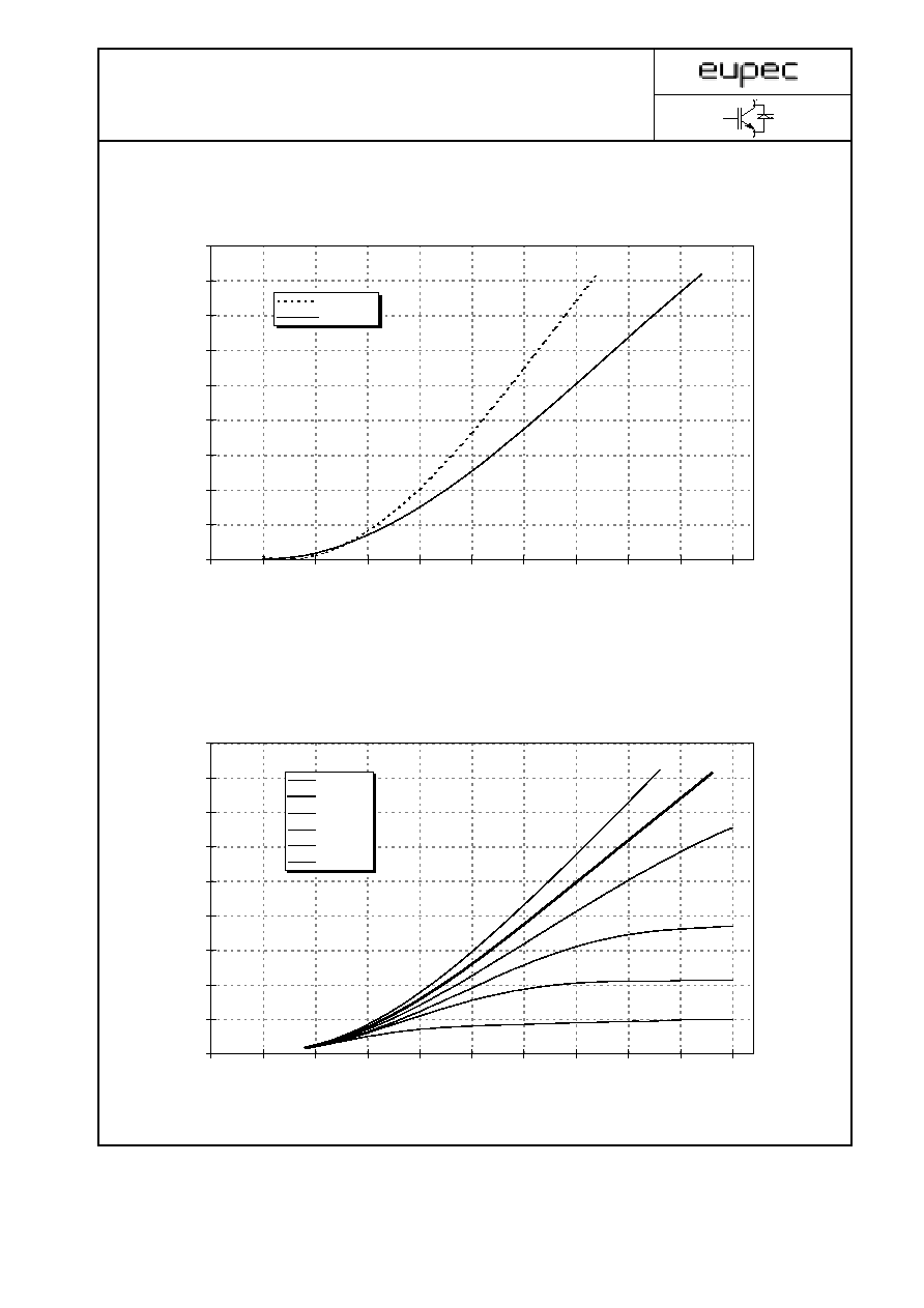
FF 401 R 17 KF6C B2
vorlšufige Daten
preliminary data
I
C
[A]
V
CE
[V]
I
C
[A]
V
CE
[V]
0
100
200
300
400
500
600
700
800
900
0,0
0,5
1,0
1,5
2,0
2,5
3,0
3,5
4,0
4,5
5,0
Tvj = 25įC
Tvj = 125įC
Ausgangskennlinie (typisch) I
C
= f (V
CE
)
Output characteristic (typical)
V
GE
= 15V
0
100
200
300
400
500
600
700
800
900
0,0
0,5
1,0
1,5
2,0
2,5
3,0
3,5
4,0
4,5
5,0
vGE = 20V
vGE = 15V
vGE = 12V
vGE = 10V
vGE = 9V
vGE = 8V
Ausgangskennlinienfeld (typisch) I
C
= f (V
CE
)
Output characteristic (typical)
T
vj
= 125įC
4(8)
FF401R17KF6CB2_V.xls

Technische Information / Technical Information
IGBT-Module
IGBT-Modules
FF 401 R 17 KF6C B2
vorlšufige Daten
preliminary data
I
C
[A]
V
GE
[V]
I
F
[A]
V
F
[V]
0
100
200
300
400
500
600
700
800
900
5
6
7
8
9
10
11
12
13
Tj = 25įC
Tj = 125įC
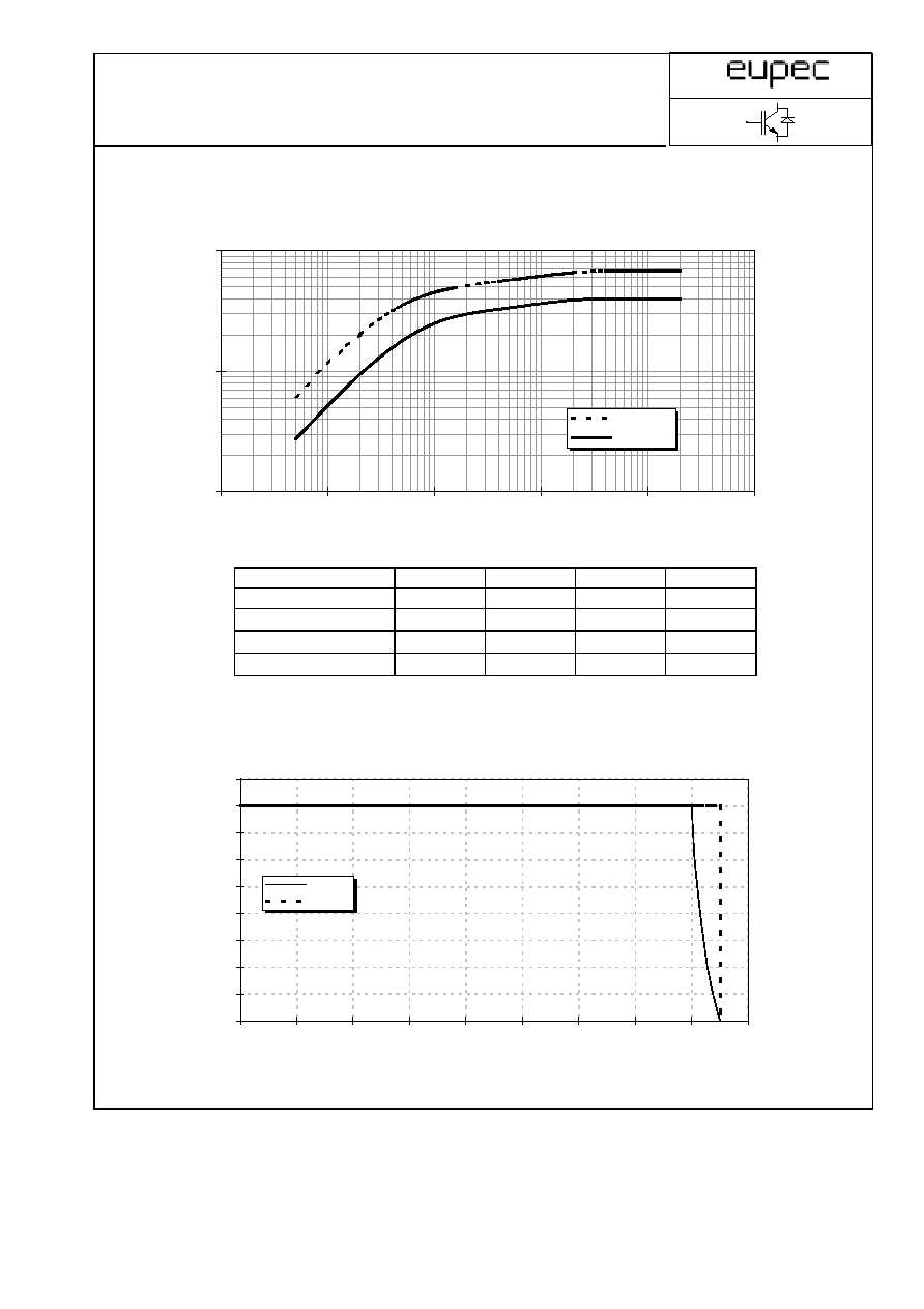
‹bertragungscharakteristik (typisch) I
C
= f (V
GE
)
Transfer characteristic (typical)
V
CE
= 20V
0
100
200
300
400
500
600
700
800
900
0,0
0,5
1,0
1,5
2,0
2,5
3,0
Tvj = 25įC
Tvj = 125įC
DurchlaŖkennlinie der Inversdiode (typisch) I
F
= f (V
F
)
Forward characteristic of inverse diode (typical)
5(8)
FF401R17KF6CB2_V.xls

Technische Information / Technical Information
IGBT-Module
IGBT-Modules
FF 401 R 17 KF6C B2
vorlšufige Daten
preliminary data
E [
m
J]
I
C
[A]
E [
m
J]
R
G
[
9
9
9
9
]
0
100
200
300
400
500
600
700
800
900
0
100
200
300
400
500
600
700
800
900
Eoff
Eon
Erec
Schaltverluste (typisch) E
on
= f (I
C
) , E
off
= f (I
C
) , E
rec
= f (I
C
)
Switching losses (typical)
R
gon
= 1,8
9
9
9
9
, R
goff
=3,6
9
9
9
9
, V
CE
= 900V, T
j
= 125įC, V
GE
= Ī 15V
0
100
200
300
400
500
600
0
4
8
12
16
20
Eoff
Eon
Erec
Schaltverluste (typisch) E
on
= f (R
G
) , E
off
= f (R
G
) , E
rec
= f (R
G
)
Switching losses (typical)
I
C
= 400A , V
CE
= 900V , T
j
= 125įC, V
GE
= Ī 15V
6(8)
FF401R17KF6CB2_V.xls
Technische Information / Technical Information
IGBT-Module
IGBT-Modules
FF 401 R 17 KF6C B2
vorlšufige Daten
preliminary data
Z
thJ
C
[
K
/ W
]
t [sec]
i
1
2
3
4
r
i
[K/kW]
: IGBT
3,76
18,86
5,7
11,6
J
i
[sec]
: IGBT
0,027
0,052
0,09
0,838
r
i
[K/kW]
: Diode
31,39
14,05
4,477
18,08
J
i
[sec]
: Diode
0,0287
0,0705
0,153
0,988
I
C
[A]
V
CE
[V]
Sicherer Arbeitsbereich (RBSOA)
Reverse bias safe operation area (RBSOA)
R
g
= 3,6 Ohm, T
vj
= 125įC
Transienter Wšrmewiderstand Z
thJC
= f (t)
Transient thermal impedance
0
100
200
300
400
500
600
700
800
900
0
200
400
600
800
1000
1200
1400
1600
1800
IC,Modul
IC,Chip
0,001
0,01
0,1
0,001
0,01
0,1
1
10
100
Zth:Diode
Zth:IGBT
7(8)
FF401R17KF6CB2_V.xls
Technische Information / Technical Information
IGBT-Module
IGBT-Modules
FF 401 R 17 KF6C B2
vorlšufige Daten
ńuŖere Abmessungen / external dimensions
preliminary data
7
4 deep
C1
C2/E1 G1
57
73
E1/C2
for M5
9,75
G2 E2
5
C1
E2
27,15
27,15
DD...
FF...
FD...
screwing depth
max. 16
26,4
5,5
2,8x0,5
C1 (K1)
E2 (A2)
E1/C2
(A1/K2)
C1
G1
G2
E2
C1
E2
C2/E1
E1/C2
C1
G1
C1
E2 (A2)
C2/E1
E1/C2
(K2)
8(8)
FF401R17KF6CB2_V.xls