
Technische Information / Technical Information
IGBT-Module
IGBT-Modules
FP40R12KE3G
Elektrische Eigenschaften / Electrical properties
Hˆchstzul‰ssige Werte / Maximum rated values
Diode Gleichrichter/ Diode Rectifier
Periodische R¸ckw. Spitzensperrspannung
repetitive peak reverse voltage
T
vj
= 25∞C
V
RRM
1600
V
Gleichrichter Ausgang Grenzeffektivstrom
maximum RMS current at Rectifier output
T
C
= 80∞C
I
RMSmax
75
A
Durchlaþstrom Grenzeffektivwert proChip
Forward current RMS maximum per Chip
T
C
= 80∞C
I
FRMSM
50
A
Stoþstrom Grenzwert
t
P
= 10 ms, T
vj
= 25∞C
I
FSM
315
A
surge forward current
t
P
= 10 ms, T
vj
= 150∞C
260
A
Grenzlastintegral
t
P
= 10 ms, T
vj
= 25∞C
I
2
t
500
A
2
s
I
2
t - value
t
P
= 10 ms, T
vj
= 150∞C
340
A
2
s
Transistor Wechselrichter/ Transistor Inverter
Kollektor-Emitter-Sperrspannung
collector-emitter voltage
T
vj
= 25∞C
V
CES
1200
V
Kollektor-Dauergleichstrom
Tc = 80 ∞C
I
C,nom.
40
A
DC-collector current
T
C
= 25 ∞C
I
C
55
A
Periodischer Kollektor Spitzenstrom
repetitive peak collector current
t
P
= 1 ms, T
C
= 80 ∞C
I
CRM
80
A
Gesamt-Verlustleistung
total power dissipation
T
C
= 25∞C
P
tot
200
W
Gate-Emitter-Spitzenspannung
gate-emitter peak voltage
V
GES
+/- 20V
V
Diode Wechselrichter/ Diode Inverter
Dauergleichstrom
DC forward current
I
F
40
A
Periodischer Spitzenstrom
repetitive peak forw. current
t
P
= 1 ms
I
FRM
80
A
Grenzlastintegral
I
2
t - value
V
R
= 0V, t
p
= 10ms, T
vj
= 125∞C
I
2
t
320
A
2
s
Transistor Brems-Chopper/ Transistor Brake-Chopper
Kollektor-Emitter-Sperrspannung
collector-emitter voltage
T
vj
= 25∞C
V
CES
1200
V
Kollektor-Dauergleichstrom
T
C
= 80 ∞C
I
C,nom.
40
A
DC-collector current
T
C
= 25 ∞C
I
C
55
A
Periodischer Kollektor Spitzenstrom
repetitive peak collector current
t
P
= 1 ms, T
C
= 80∞C
I
CRM
80
A
Gesamt-Verlustleistung
total power dissipation
T
C
= 25∞C
P
tot
200
W
Gate-Emitter-Spitzenspannung
gate-emitter peak voltage
V
GES
+/- 20V
V
Diode Brems-Chopper/ Diode Brake-Chopper
Dauergleichstrom
DC forward current
I
F
15
A
Periodischer Spitzenstrom
repetitive peak forw. current
t
P
= 1 ms
I
FRM
30
A
prepared by: Andreas Schulz
date of publication:23.04.2002
approved by: Robert Severin
revision: 2
1(11)
DB-PIM-IGBT3_2Serie.xls

Technische Information / Technical Information
IGBT-Module
IGBT-Modules
FP40R12KE3G
Modul Isolation/ Module Isolation
Isolations-Pr¸fspannung
insulation test voltage
RMS, f = 50 Hz, t = 1 min.
NTC connected to Baseplate
V
ISOL
2,5
kV
Elektrische Eigenschaften / Electrical properties
Charakteristische Werte / Characteristic values
Diode Gleichrichter/ Diode Rectifier
min.
typ.
max.
Durchlaþspannung
forward voltage
T
vj
= 150∞C, I
F
= 40 A
V
F
-
1,2
-
V
Schleusenspannung
threshold voltage
T
vj
= 150∞C
V
(TO)
-
-
0,8
V
Ersatzwiderstand
slope resistance
T
vj
= 150∞C
r
T
-
-
10,5
m
Sperrstrom
reverse current
T
vj
= 150∞C, V
R
= 1600 V
I
R
-
2
-
mA
Modul Leitungswiderstand, Anschl¸sse-Chip
lead resistance, terminals-chip
T
C
= 25∞C
R
AA'+CC'
-
4
-
m
Transistor Wechselrichter/ Transistor Inverter
min.
typ.
max.
Kollektor-Emitter S‰ttigungsspannung
V
GE
= 15V, T
vj
= 25∞C, I
C
=
40 A
V
CE sat
-
1,8
2,3
V
collector-emitter saturation voltage
V
GE
= 15V, T
vj
= 125∞C, I
C
=
40 A
-
2,15
-
V
Gate-Schwellenspannung
gate threshold voltage
V
CE
= V
GE
, T
vj
= 25∞C, I
C
=
1,5 mA
V
GE(TO)
5,0
5,8
6,5
V
Eingangskapazit‰t
input capacitance
f = 1MHz, T
vj
= 25∞C
V
CE
= 25 V, V
GE
= 0 V
C
ies
-
2,5
-
nF
Kollektor-Emitter Reststrom
collector-emitter cut off current
V
GE
= 0V, T
vj
= 25∞C, V
CE
=
1200 V
I
CES
-
-
5
mA
Gate-Emitter Reststrom
gate-emitter leakage current
V
CE
= 0V, V
GE
=20V, T
vj
=25∞C
I
GES
-
-
400
nA
Einschaltverzˆgerungszeit (ind. Last)
I
C
= I
Nenn
, V
CC
= 600 V
turn on delay time (inductive load)
V
GE
= ±15V, T
vj
= 25∞C, R
G
=
27 Ohm
t
d,on
-
85
-
ns
V
GE
= ±15V, T
vj
= 125∞C, R
G
=
27 Ohm
-
90
-
ns
Anstiegszeit (induktive Last)
I
C
= I
Nenn
, V
CC
= 600 V
rise time (inductive load)
V
GE
= ±15V, T
vj
= 25∞C, R
G
=
27 Ohm
t
r
-
30
-
ns
V
GE
= ±15V, T
vj
= 125∞C, R
G
=
27 Ohm
-
45
-
ns
Abschaltverzˆgerungszeit (ind. Last)
I
C
= I
Nenn
, V
CC
= 600 V
turn off delay time (inductive load)
V
GE
= ±15V, T
vj
= 25∞C, R
G
=
27 Ohm
t
d,off
-
420
-
ns
V
GE
= ±15V, T
vj
= 125∞C, R
G
=
27 Ohm
-
520
-
ns
Fallzeit (induktive Last)
I
C
= I
Nenn
, V
CC
= 600 V
fall time (inductive load)
V
GE
= ±15V, T
vj
= 25∞C, R
G
=
27 Ohm
t
f
-
65
-
ns
V
GE
= ±15V, T
vj
= 125∞C, R
G
=
27 Ohm
-
90
-
ns
Einschaltverlustenergie pro Puls
I
C
= I
Nenn
, V
CC
= 600 V
turn-on energy loss per pulse
V
GE
= ±15V, T
vj
= 125∞C, R
G
=
27 Ohm
E
on
-
6
-
mWs
L
= 45 nH
Abschaltverlustenergie pro Puls
I
C
= I
Nenn
, V
CC
= 600 V
turn-off energy loss per pulse
V
GE
= ±15V, T
vj
= 125∞C, R
G
=
27 Ohm
E
off
-
4,2
-
mWs
L
= 45 nH
Kurzschluþverhalten
t
P
10µs, V
GE
15V, R
G
=
27 Ohm
SC Data
T
vj
125∞C, V
CC
=
720 V
I
SC
-
160
-
A
2(11)
DB-PIM-IGBT3_2Serie.xls

Technische Information / Technical Information
IGBT-Module
IGBT-Modules
FP40R12KE3G
Elektrische Eigenschaften / Electrical properties
Charakteristische Werte / Characteristic values
min.
typ.
max.
Modulinduktivit‰t
stray inductance module
L
CE
-
-
60
nH
Modul Leitungswiderstand, Anschl¸sse-Chip
lead resistance, terminals-chip
T
C
= 25∞C
R
CC'+EE'
-
7
-
m
Diode Wechselrichter/ Diode Inverter
min.
typ.
max.
Durchlaþspannung
V
GE
= 0V, T
vj
= 25∞C, I
F
= 40 A
V
F
-
1,75
2,3
V
forward voltage
V
GE
= 0V, T
vj
= 125∞C, I
F
= 40 A
-
1,75
-
V
R¸ckstromspitze
I
F
=I
Nenn
, - di
F
/dt = 900 A/µs
peak reverse recovery current
V
GE
= -10V, T
vj
= 25∞C, V
R
=
600 V
I
RM
-
39
-
A
V
GE
= -10V, T
vj
= 125∞C, V
R
=
600 V
-
38
-
A
Sperrverzˆgerungsladung
I
F
=I
Nenn
, - di
F
/dt = 900 A/µs
recovered charge
V
GE
= -10V, T
vj
= 25∞C, V
R
=
600 V
Q
r
-
4,2
-
µAs
V
GE
= -10V, T
vj
= 125∞C, V
R
=
600 V
-
7,8
-
µAs
Abschaltenergie pro Puls
I
F
=I
Nenn
, - di
F
/dt = 900 A/µs
reverse recovery energy
V
GE
= -10V, T
vj
= 25∞C, V
R
=
600 V
E
rec
-
1,35
-
mWs
V
GE
= -10V, T
vj
= 125∞C, V
R
=
600 V
-
2,8
-
mWs
Transistor Brems-Chopper/ Transistor Brake-Chopper
min.
typ.
max.
Kollektor-Emitter S‰ttigungsspannung
V
GE
= 15V, T
vj
= 25∞C, I
C
=
40 A
V
CE sat
-
1,8
2,3
V
collector-emitter saturation voltage
V
GE
= 15V, T
vj
= 125∞C, I
C
=
40 A
-
2,15
-
V
Gate-Schwellenspannung
gate threshold voltage
V
CE
= V
GE
, T
vj
= 25∞C, I
C
=
1,5 mA
V
GE(TO)
5,0
5,8
6,5
V
Eingangskapazit‰t
input capacitance
f = 1MHz, T
vj
= 25∞C
V
CE
= 25 V, V
GE
= 0 V
C
ies
-
2,5
-
nF
Kollektor-Emitter Reststrom
collector-emitter cut off current
V
GE
= 0V, T
vj
= 25∞C, V
CE
=
1200 V
I
CES
-
5,0
500
mA
Gate-Emitter Reststrom
gate-emitter leakage current
V
CE
= 0V, V
GE
= 20V, T
vj
= 25∞C
I
GES
-
-
400
nA
Schaltverluste und -bedingungen
Switching losses and conditions
Diode Brems-Chopper/ Diode Brake-Chopper
min.
typ.
max.
Durchlaþspannung
T
vj
= 25∞C, I
F
=
40 A
V
F
-
2,35
2,8
V
forward voltage
T
vj
= 125∞C, I
F
=
40 A
-
2,55
-
V
Schaltverluste und -bedingungen
Switching losses and conditions
NTC-Widerstand/ NTC-Thermistor
min.
typ.
max.
Nennwiderstand
rated resistance
T
C
= 25∞C
R
25
-
5
-
k
Abweichung von R
100
deviation of R
100
T
C
= 100∞C, R
100
= 493
R/R
-5
5
%
Verlustleistung
power dissipation
T
C
= 25∞C
P
25
20
mW
B-Wert
B-value
R
2
= R
1
exp [B(1/T
2
- 1/T
1
)]
B
25/50
3375
K
siehe Wechselrichter in diesem Datenblatt
see inverter in this datasheet
siehe Wechselrichter in Dbl FP15R12KE3
see inverter in datasheet FP15R12KE3
3(11)
DB-PIM-IGBT3_2Serie.xls

Technische Information / Technical Information
IGBT-Module
IGBT-Modules
FP40R12KE3G
Thermische Eigenschaften / Thermal properties
min.
typ.
max.
Innerer W‰rmewiderstand
Gleichr. Diode/ Rectif. Diode
R
thJC
-
-
1
K/W
thermal resistance, junction to case
Trans. Wechsr./ Trans. Inverter
-
-
0,6
K/W
Diode Wechsr./ Diode Inverter
-
-
0,95
K/W
Trans. Bremse/ Trans. Brake
-
-
0,6
K/W
Diode Bremse/ Diode Brake
-
-
1,5
K/W
Ðbergangs-W‰rmewiderstand
Gleichr. Diode/ Rectif. Diode
Paste
=1W/m*K
R
thCK
-
0,04
-
K/W
thermal resistance, case to heatsink
Trans. Wechsr./ Trans. Inverter
grease
=1W/m*K
-
0,02
-
K/W
Diode Wechsr./ Diode Inverter
-
0,04
-
K/W
Hˆchstzul‰ssige Sperrschichttemperatur
maximum junction temperature
T
vj
-
-
150
∞C
Betriebstemperatur
operation temperature
T
op
-40
-
125
∞C
Lagertemperatur
storage temperature
T
stg
-40
-
125
∞C
Mechanische Eigenschaften / Mechanical properties
Innere Isolation
internal insulation
Al
2
O
3
CTI
comperative tracking index
225
Anzugsdrehmoment f. mech. Befestigung
Schraube M 5
M
3
-
6
Nm
mounting torque
screw M 5
Gewicht
weight
G
300
g
Luftstrecke
clearance
Pin-Erde
Pin-GND
7,5
mm
Kriechstrecke
creeping distance
Pin-Erde
Pin-GND
10
mm
Transiente Thermische Eigenschaften / Transient Thermal properties
r
i
[K/W]
1
6,769E-02
2
1,052E-01
3
2,709E-01
4
1,523E-01
2,820E-02
1,128E-01
1,800E-01
5,701E-02
1,294E-01
7,662E-01
IGBT-Wechselrichter
IGBT-Inverter
Diode-Wechselrichter
Diode-Inverter
r
i
[K/W]
i
[s]
i
[s]
2,820E-01
3,429E-02
2,345E-03
3,333E-03
9,674E-02
6,249E-01
4(11)
DB-PIM-IGBT3_2Serie.xls

Technische Information / Technical Information
IGBT-Module
IGBT-Modules
FP40R12KE3G
I
C
[A]
V
CE
[V]
I
C
[A]
V
CE
[V]
Ausgangskennlinienfeld Wechselr. (typisch) I
C
= f (V
CE
)
Output characteristic Inverter (typical)
V
GE
= 15 V
0
10
20
30
40
50
60
70
80
0
0,5
1
1,5
2
2,5
3
3,5
4
4,5
5
Tvj = 25∞C
Tvj = 125∞C
0
10
20
30
40
50
60
70
80
0
0,5
1
1,5
2
2,5
3
3,5
4
4,5
5
Vge=19V
Vge=17V
Vge=15V
Vge=13V
Vge=11V
Vge=9V
Ausgangskennlinienfeld Wechselr. (typisch) I
C
= f (V
CE
)
Output characteristic Inverter (typical)
T
vj
= 125∞C
5(11)
DB-PIM-IGBT3_2Serie.xls

Technische Information / Technical Information
IGBT-Module
IGBT-Modules
FP40R12KE3G
I
C
[A]
V
GE
[V]
I
F
[A]
V
F
[V]
Durchlaþkennlinie der Freilaufdiode Wechselr. (typisch) I
F
= f (V
F
)
Forward characteristic of FWD Inverter (typical)
0
10
20
30
40
50
60
70
80
0
2
4
6
8
10
12
14
Tvj=25∞C
Tvj=125∞C
Ðbertragungscharakteristik Wechselr. (typisch) I
C
= f (V
GE
)
Transfer characteristic Inverter (typical)
V
CE
= 20 V
0
10
20
30
40
50
60
70
80
0
0,5
1
1,5
2
2,5
3
Tvj = 25∞C
Tvj = 125∞C
6(11)
DB-PIM-IGBT3_2Serie.xls
Technische Information / Technical Information
IGBT-Module
IGBT-Modules
FP40R12KE3G
600 V
27 Ohm
E [
m
W
s
]
I
C
[A]
600 V
E [
m
W
s
]
R
G
[
]
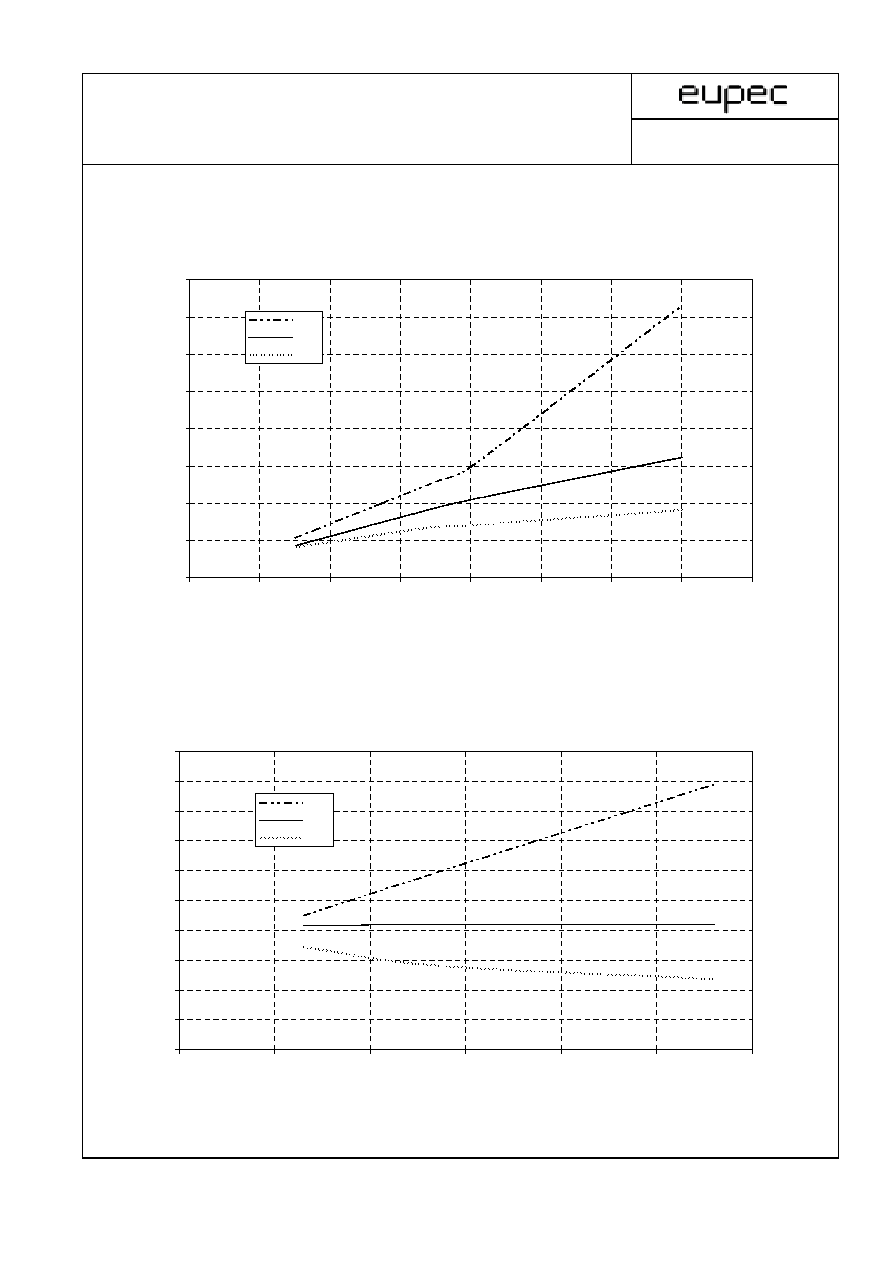
Schaltverluste Wechselr. (typisch) E
on
= f (I
C
), E
off
= f (I
C
), E
rec
= f (I
C
)
V
CC
=
Switching losses Inverter (typical)
T
j
= 125∞C, V
GE
= ±15 V, R
Gon
= R
Goff
=
0
2
4
6
8
10
12
14
16
0
10
20
30
40
50
60
70
80
Eon
Eoff
Erec
0
1
2
3
4
5
6
7
8
9
10
0
10
20
30
40
50
60
Eon
Eoff
Erec
Schaltverluste Wechselr. (typisch) E
on
= f (R
G
), E
off
= f (R
G
), E
rec
= f (R
G
)
Switching losses Inverter (typical)
T
j
= 125∞C, V
GE
= +-15 V , I
c
= I
nenn
, V
CC
=
7(11)
DB-PIM-IGBT3_2Serie.xls

Technische Information / Technical Information
IGBT-Module
IGBT-Modules
FP40R12KE3G
Z
thJ
C
[
K
/W
]
t [s]
I
C
[A]
V
CE
[V]
Transienter W‰rmewiderstand Wechselr. Z
thJC
= f (t)
Transient thermal impedance Inverter
0,01
0,1
1
0,001
0,01
0,1
1
10
Zth-IGBT
Zth-FWD
0
10
20
30
40
50
60
70
80
90
0
200
400
600
800
1000
1200
1400
IC,Modul
IC,Chip
Ri und ti-Werte siehe S. 4
Ri and ti-Values see P. 4
Sicherer Arbeitsbereich IGBT-Wechselr. (RBSOA)
Reverse bias save operating area (RBSOA)
V
GE
= 15V, T
j
= 125∞C
8(11)
DB-PIM-IGBT3_2Serie.xls

Technische Information / Technical Information
IGBT-Module
IGBT-Modules
FP40R12KE3G
I
C
[A]
V
CE
[V]
I
F
[A]
V
F
[V]
0
10
20
30
40
50
60
70
80
0
0,5
1
1,5
2
2,5
3
3,5
4
4,5
5
Tvj = 25∞C
Tvj = 125∞C
Durchlaþkennlinie der Brems-Chopper-Diode (typisch) I
F
= f (V
F
)
Forward characteristic of brake-chopper-FWD (typical)
Ausgangskennlinienfeld Brems-Chopper-IGBT (typisch)
I
C
= f (V
CE
)
Output characteristic brake-chopper-IGBT (typical)
V
GE
= 15 V
0
10
20
30
40
50
60
70
80
0
0,5
1
1,5
2
2,5
3
3,5
4
Tvj = 25∞C
Tvj = 125∞C
9(11)
DB-PIM-IGBT3_2Serie.xls

Technische Information / Technical Information
IGBT-Module
IGBT-Modules
FP40R12KE3G
I
F
[A]
V
F
[V]
R[
]
T
C
[∞C]
Durchlaþkennlinie der Gleichrichterdiode (typisch) I
F
= f (V
F
)
Forward characteristic of Rectifier Diode (typical)
0
10
20
30
40
50
60
70
80
0
0,2
0,4
0,6
0,8
1
1,2
1,4
1,6
1,8
Tvj = 25∞C
Tvj = 150∞C
NTC- Temperaturkennlinie (typisch) R = f (T)
NTC- temperature characteristic (typical)
Rtyp
100
1000
10000
100000
0
20
40
60
80
100
120
140
160
10(11)
DB-PIM-IGBT3_2Serie.xls

Technische Information / Technical Information
IGBT-Module
IGBT-Modules
FP40R12KE3G
Schaltplan/ Circuit diagram
Geh‰useabmessungen/ Package outlines
Mit dieser technischen Information werden Halbleiterbauelemente spezifiziert, jedoch keine
Eigenschaften zugesichert. Sie gilt in Verbindung mit den zugehˆrigen Technischen Erl‰uterungen.
This technical information specifies semiconductor devices but promises no characteristics. It is
valid in combination with the belonging technical notes.
2
3
1
21
23
22
24
20
19
13
4
16
15
11
18
17
12
5
6
10
7
14
NTC
9
8
11(11)
DB-PIM-IGBT3_2Serie.xls