FZ 1800 R 12 KF4
H�chstzul�ssige Werte / Maximum rated values
Elektrische Eigenschaften / Electrical properties
Kollektor-Emitter-Sperrspannung
collector-emitter voltage
V
CES
1200 V
Kollektor-Dauergleichstrom
DC-collector current
I
C
1800 A
Period. Kollektor Spitzenstrom
repetitive peak collector current
t
p
=1 ms
I
CRM
3600 A
Gesamt-Verlustleistung
total power dissipation
t
C
=25�C, Transistor
P
tot
11 kW
Gate-Emitter-Spitzenspannung
gate-emitter peak voltage
V
GE
+/- 20 V
Dauergleichstrom
DC forward current
I
F
1800 A
Periodischer Spitzenstrom
repetitive peak forw. current
t
p
=1ms
I
FRM
3600 A
Isolations-Pr�fspannung
insulating test voltage
RMS, f=50 Hz, t= 1 min.
V
ISOL
2,5 kV
Charakteristische Werte / Characteristic values: Transistor
min.
typ.
max
Koll.-Emitter S�ttigungsspannung
coll.-emitter saturation voltage
i
C
=1,8kA, v
GE
=15V, t
vj
=25�C
v
CE sat
-
2,7
3,2 V
i
C
=1,8kA,v
GE
=15V,t
vj
=125�C
-
3,3
3,9 V
Gate-Schwellspannung
gate threshold voltage
i
C
=72mA,v
CE
=v
GE
,t
vj
=25�C
v
GE(th)
4,5
5,5
6,5 V
Eingangskapazit�t
input capacity
f
O
=1MHz,t
vj
=25�C,v
CE
=25V,
v
GE
=0
C
ies
-
135
- nF
Kollektor-Emitter Reststrom
collector-emitter cut-off current
v
CE
=1200V,v
GE
=0V,t
vj
=25�C
i
CES
-
-
30 mA
v
CE
=1200V,v
GE
=0V,t
vj
=125�C
-
-
300 mA
Gate-Emitter Reststrom
gate leakage current
v
CE
=0V, v
GE
=20V, t
vj
=25�C
i
GES
-
-
400 nA
Emitter-Gate Reststrom
gate leakage current
v
CE
=0V, v
EG
=20V, t
vj
=25�C
i
EGS
-
-
400 nA
Einschaltzeit (ohmsche Last)
turn-on time (resistive load)
i
C
=1,8kA,v
CE
=6
00
V,v
L
=15V
t
on
v
L
=15V,R
G
=0,43
,t
vj
=25�C
-
-
- �s
t
vj
=125�C
-
-
- �s
Speicherzeit (induktive Last)
storage time
i
C
=1,8kA,v
CE
=6
00
V,v
L
=15V
t
s
v
L
=15V,R
G
=0,43
,t
vj
=25�C
-
-
- �s
t
vj
=125�C
-
-
- �s
Fallzeit (induktive Last)
fall time (inductive load)
i
C
=1,8kA,v
CE
=6
00
V,v
L
=15V
t
f
v
L
=15V,R
G
=0,43
,t
vj
=25�C
-
-
- �s
t
vj
=125�C
-
-
- �s
Bedingungen f�r den Kurzschlu�schutz / Conditions for short-circuit protection
t
fg
= 10�s
V
CC
= 750V
v
L
= � 15V
v
CEM
= 900V
R
GF
= R
GR
=0,43
i
CMK1
= 18000V
t
vj
= 125�C
i
CMK2
= 13500V
Unabh�ngig davon dilt bei abweichenden Bedingungen / with regard to other conditions
v
CEM
= V
CES
- 12nH . |di
C
/dt|
Charakteristische Werte / Characteristic values: Invers-Diode
Durchla�spannung
forward voltage
i
F
=1,8kA, v
GE
=0V, t
vj
=25�C
V
F
-
2,2
2,7 V
i
F
=1,8kA, v
GE
=0V, t
vj
=125�C
-
2
2,5 V
R�ckstromspitze
peak reverse recovery current
i
F
=1,8kA, -di
F
/dt=1,8kA/�s
I
RM
v
RM
=6
00
V,v
EG
=10V,t
vj
=25�C
-
-
- A
v
RM
=6
00
V,v
EG
=10V,t
vj
=125�C
-
-
- A
Sperrverz�gerungsladung
recovered charge
i
F
=1,8kA, -di
F
/dt=1,8kA/�s
Q
r
v
RM
=6
00
V,v
EG
=10V,t
vj
=25�C
-
-
- �As
v
RM
=6
00
V,v
EG
=10V,t
vj
=125�C
-
-
- �As
Thermische Eigenschaften / Thermal properties
Innerer W�rmewiderstand
thermal resist., junction to case
Transistor / transistor, DC
R
thJC
0,011 �C/W
Diode, DC
0,024 �C/W
�bergangs-W�rmewiderstand
thermal resist., case to heatsink
pro Module / per Module
R
thCK
0,006 �C/W
H�chstzul. Sperrschichttemp.
max. junction temperature
Transistor
t
vj max
150 �C
Betriebstemperatur
operating temperature
Transistor / transistor
t
c op
-40...+125 �C
Lagertemperatur
storage temperature
t
stg
-40...+125 �C
Mechanische Eigenschaften / Mechanical properties
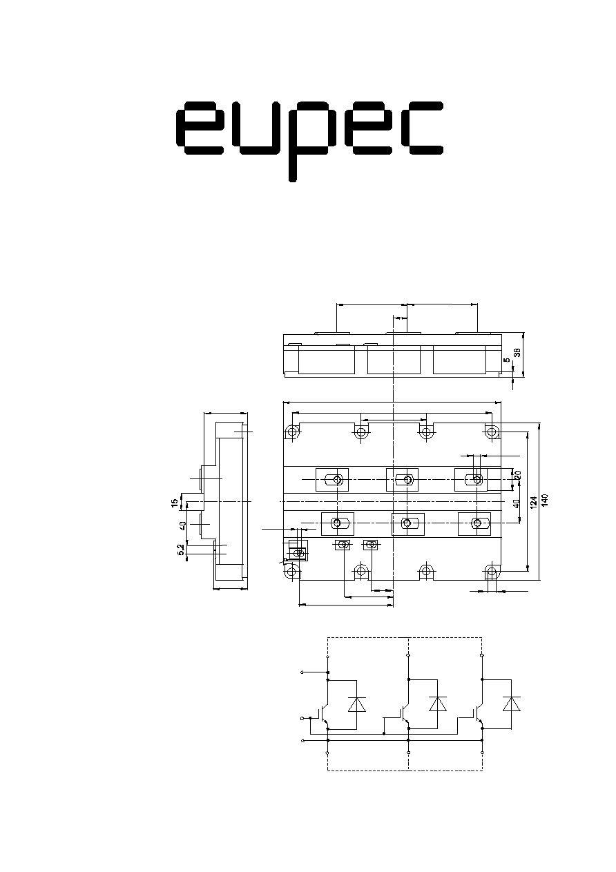
Geh�use, siehe Anlage
case, see appendix
Seite / page
1
Innere Isolation
internal insulation
Al
2
O
3
Anzugsdrehm. f. mech. Befest.
mounting torque
M1
3 Nm
Anzugsdrehm. f. elektr. Anschl.
terminal connection torque
terminals M4
M2
2 Nm
terminals M8
8...10 Nm
Gewicht
weight
G
ca.2300 g
Mit dieser technischen Information werden Halbleiterbauelemente spezifiziert, jedoch keine Eigenschaften zugesichert. Sie gilt in Verbindung mit den zugeh�rigen technischen Erl�uterungen.
This technical information specifies semiconductor devices but promises no characteristics. It is valid in combination with the belonging technical notes.
eupec GmbH + Co KG, Max-Plank-Str. 5, D59581 Warstein, Telefon +49 (0)2902/764-0, Telefax /764-
256
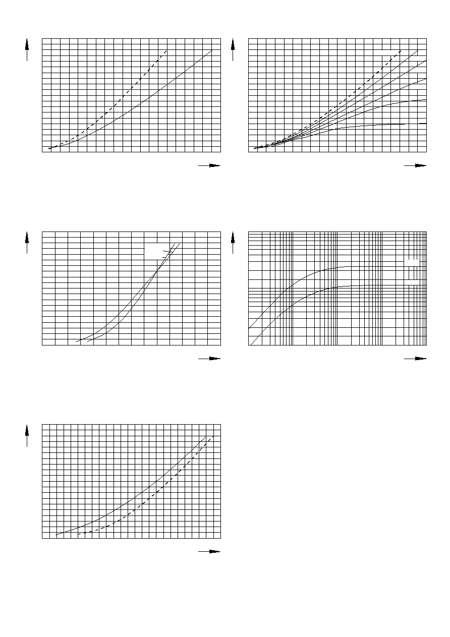
Bild / Fig. 1
Kollektor-Emitter-Spannung im S�ttigungsbereich (typisch)
Collector-emitter-voltage in saturation region (typical)
V
GE
= 15V
- - - - t
vj
= 25�C
____ t
vj
= 125�C
Bild / Fig. 2
Kollektor-Emitter-Spannung im S�ttigungsbereich (typisch)
Collector-emitter-voltage in saturation region (typical)
t
vj
= 125�C
Bild / Fig. 3
�bertragungscharakteristik (typisch)
Transfer characteristic (typical)
V
CE
= 20V
Bild / Fig. 4
Transienter innerer W�rmewiderstand (DC)
Transient thermal impedance (DC)
Bild / Fig. 5
Durchla�kennlinie der Inversdiode (typisch)
Forward charakteristic of the inverse diode (typical)
----- t
vj
= 25�C
___ t
vj
= 125�C
4000
1
v
CE
[V]
0
2
3
4
5
2000
3000
1000
i
C
[A]
FZ 1800 R 12 KF4
4000
1
v
CE
[V]
0
2
3
4
5
2000
3000
1000
i
C
[A]
FZ 1800 R 12 KF4
V
GE
=20V
15V
12V
10V
9V
8V
4000
5
v
GE
[V]
0
2000
3000
1000
i
C
[A]
6
7
8
9
10
11
11
12
t
vj
=
125�C
25�C
FZ 1800 R 12 KF4
t [s]
Z
(th)JC
[�C/W]
10
-3
10
1
10
-2
10
-1
2
4
6
2
4
6
2
4
6
2
4
6
10
-3
2
4
6
8
10
-2
2
4
6
8
10
-1
Diode
IGBT
FZ 1800 R 12 KF4
10
0
4000
0,5
v
F
[V]
0
2000
3000
1000
i
F
[A]
1,0
1,5
2,0
2,5
3,0
FZ 1800 R 12 KF4
FZ 1800 R 12 KF4