 | –≠–ª–µ–∫—Ç—Ä–æ–Ω–Ω—ã–π –∫–æ–º–ø–æ–Ω–µ–Ω—Ç: TD131N | –°–∫–∞—á–∞—Ç—å:  PDF PDF  ZIP ZIP |
VWK February 1996
Marketing Information
TT 131 N
plug
A 2,8 x 0,8
max. 12
screwing depth
M6x15 Z4-1
for fillister head screw
K1
K2
25
25
15
80
94
5
13,3
14
G2
G1
AK K
A
K1 G1
K2 G2
European Power-
Semiconductor and
Electronics Company
GmbH + Co. KG

TT 131 N, TD 131 N, DT 131 N
Elektrische Eigenschaften
Electrical properties
Hˆchstzul‰ssige Werte
Maximum rated values
Periodische Vorw‰rts- und
R¸ckw‰rts-Spitzensperrspannung
repetitive peak forward off-state and
reverse voltages
t
vj
= -40∞C...t
vj max
V
DRM
, V
RRM
600 800 1000
1200 1400
V
Vorw‰rts-Stoþspitzensperrspannung non-repetitive peak forward off-state
voltage
t
vj
= -40∞C...t
vj max
V
DSM
= V
DRM
V
R¸ckw‰rts-
Stoþspitzensperrspannung
non-repetitive peak reverse voltage t
vj
= +25∞C...t
vj max
V
RSM
= V
RRM
+ 100 V
Durchlaþstrom-Grenzeffektivwert
RMS on-state current
I
TRMSM
220 A
Dauergrenzstrom
average on-state current
t
c
= 85∞C
I
TAVM
131 A
t
c
= 81∞C
140 A
Stoþstrom-Grenzwert
surge current
t
vj
= 25∞C, t
p
= 10 ms
I
TSM
3600 A
t
vj
= t
vj max
, t
p
= 10 ms
3200 A
Grenzlastintegral
i
2
t-value
t
vj
= 25∞C, t
p
= 10 ms
i
2
dt
64800 A
2
s
t
vj
= t
vj max
, t
p
= 10 ms
51200 A
2
s
Kritische Stromsteilheit
current
v
D
67%, V
DRM
, f
o
= 50 Hz
(di/dt)
cr
150 A/µs
v
L
=10V,i
GM
=0,6A,di
G
/dt =0,6A/µs
Kritische Spannungssteilheit
voltage
t
vj
= t
vj max
, v
D
= 0,67 V
DRM
(dv/dt)
cr
1000 V/µs
Charakteristische Werte
Characteristic values
Durchlaþspannung
on-state voltage
t
vj
= t
vj max
, i
T
= 350 A
v
T
max.1,48 V
Schleusenspannung
threshold voltage
t
vj
= t
vj max
V
T(TO)
0,85 V
Ersatzwiderstand
slope resistance
t
vj
= t
vj max
r
T
1,5 m
Z¸ndstrom
gate trigger current
t
vj
= 25 ∞C, v
D
= 6 V
I
GT
max. 150 mA
Z¸ndspannung
gate trigger voltage
t
vj
= 25 ∞C, v
D
= 6 V
V
GT
max.1,4 V
Nicht z¸ndender Steuerstrom
gate non-trigger current
t
vj
= t
vj max
, v
D
= 6 V
I
GD
max.5 mA
Nicht z¸ndende Steuerspannung
gate non-trigger voltage
t
vj
= t
vj max
, v
D
= 0,5 V
DRM
V
GD
max.0,2 V
Haltestrom
holding current
t
vj
= 25 ∞C, v
D
= 6 V, R
A
= 5
I
H
max. 200 mA
Einraststrom
latching current
t
vj
= 25 ∞C,v
D
= 6 V, R
GK
> = 10
I
L
max. 620 mA
i
GM
= 0,6 A, di
G
/dt = 0,6 A/µs, t
g
= 20 µs
Vorw‰rts- und R¸ckw‰rts-
Sperrstrom
forward off-state and reverse
currents
t
vj
= t
vj max
, v
D
=V
DRM
, v
R
=V
RRM
i
D
, i
R
max. 25 mA
Z¸ndverzug
gate controlled delay time
t
vj
=25∞C, i
GM
= 0,6 A, di
G
/dt = 0,6 A/µs
t
gd
max.3 µs
Freiwerdezeit
circuit commutated turn-off time
siehe Techn.Er./see Techn.Inf.
t
q
typ.180 µs
Isolations-Pr¸fspannung
insulation test voltage
RMS, f = 50 Hz, t = 1 min
V
ISOL
3 kV
Thermische Eigenschaften
Thermal properties
Innerer W‰rmewiderstand
thermal resistance, junction
=180∞el,sinus: pro Modul/per module
R
thJC
max.0,115 ∞C/W
to case
pro Zweig/per arm
max.0,23 ∞C/W
DC: pro Modul/per module
max.0,107 ∞C/W
pro Zweig/per arm
max.0,214 ∞C/W
Ðbergangs-W‰rmewiderstand
thermal resistance, case to heatsink pro Modul/per module
R
thCK
max.0,03 ∞C/W
pro Zweig/per arm
max.0,06 ∞C/W
Hˆchstzul.Sperrschichttemperatur
max. junction temperature
t
vj max
125 ∞C
Betriebstemperatur
operating temperature
t
c op
-40...+125 ∞C
Lagertemperatur
storage temperature
t
stg
-40...+130 ∞C
Mechanische Eigenschaften
Mechanical properties
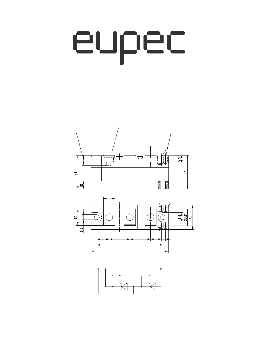
Geh‰use, siehe Seite
case, see page
1
Si-Elemente mit Druckkontakt
Si-pellet with pressure contact
Innere Isolation
internal insulation
AlN
Anzugsdrehmoment f¸r
mechanische Befestigung
mounting torque
Toleranz/tolerance +/- 15%
M1
6 Nm
Anzugsdrehmoment f¸r elektrische
Anschl¸sse
terminal connection torque
Toleranz/tolerance +5%/-10%
M2
6 Nm
Gewicht
weight
G
typ.430
g
Kriechstrecke
creepage distance
14 mm
Schwingfestigkeit
vibration resistance
f = 50 Hz
5 . 9,81 m/s≤
Diese Module kˆnnen auch mit gemeinsamer Anode oder gemeinsamer Kathode geliefert werden.
These modules can also be supplied with common anode or common cathode.
Recognized by UNDERWRITERS LABORATORIES INC.

TT 131 N
P
tot
[W]
0.1
I
d
[A]
0
0
1250
TT 131 N/6
20
40
60
80
100
100
200
t
A
[∞C]
250
500
1.0
0.8
0.6
0.5
0.4
0.25
0.2
0.15
0.12
0.08
R
thCA
[∞C/W]
0
400
1000
0.3
750
0.06
0.05 0.04
300
t
C
[∞C]
I
TAVM
[A]
0
50
60
80
100
130
TT 131 N/4
250
40
20
100
150
200
t
C
[∞C]
180∞
= 30∞
I
TAVM
[A]
0
50
100
60∞
120∞
90∞
0
TT 131 N/2
150
20
40
60
80
100
130
P
TAV
[W]
180∞
= 30∞
I
TAV
[A]
0
0
50
100
60∞
120∞
90∞
0
TT 131 N/1
150
20
40
60
80
100
120
140
200
160
180
P
TAV
[W]
I
TAV
[A]
0
0
50
50
250
TT 131 N/3
150
200
100
150
200
100
P
tot
[W]
I
d
[A]
0
0
800
TT 131 N/5
20
40
60
80
100
100
200
300
t
A
[∞C]
200
400
600
1.5
1.0
0.8
0.6
0.25
0.2
0.15
0.12
0.10
0.08
0.06
R-Last
R-load
R
thCA
[∞C/W]
L-Last
L-load
0
400
0.5
0.4
0.3
0.05
Bild / Fig. 1
Durchlaþverlustleistung je Zweig / On-state power loss per arm
P
TAV
= f(I
TAV
)
Parameter: Stromfluþwinkel / current conduction angle
Bild / Fig. 2
Hˆchstzul‰ssige Geh‰usetemperatur / Maximum allowable case temperature
t
C
= f(I
TAVM
)
Strombelastung je Zweig / current load per arm
Parameter: Stromfluþwinkel / current conduction angle
Bild / Fig. 4
Hˆchstzul‰ssige Geh‰usetemperatur / Maximum allowable case temperature
t
C
= f(I
TAVM
)
Strombelastung je Zweig / current load per arm
Parameter: Stromfluþwinkel / current conduction angle
Bild / Fig. 3
Durchlaþverlustleistung je Zweig / On-state power loss per arm
P
TAV
= f(I
TAV
)
Parameter: Stromfluþwinkel / current conduction angle
= 30∞
60∞
180∞
90∞
0
DC
120∞
120∞
= 30∞
60∞
180∞
90∞
0
DC
Bild / Fig. 6
B6 - Sechpuls-Br¸ckenschaltung / Six-pulse bridge circuit
Hˆchstzul‰ssiger Ausgangsstrom / Maximum rated output current I
d
Gesamtverlustleist. der Schaltung / Total power dissip. of the circuit P
tot
Parameter: W‰rmewiderstand zwischen Geh‰use und Umgebung /
thermal resistance case to ambient R
thCA
Bild / Fig. 5
B2 - Zweiplus-Br¸ckenschaltung / Two-pulse bridge circuit
Hˆchstzul‰ssiger Ausgangsstrom
/
Maximum rated output current I
d
Gesamtverlustleist. der Schaltung / total power dissip. of the circuit P
tot
Parameter: W‰rmewiderstand zwischen Geh‰use und Umgebung /
thermal resistance case to ambient R
thCA

TT 131 N
P
tot
[W]
I
RMS
[A]
0
0
400
TT 131 N/7
20
40
60
80
100
100
200
300
t
A
[∞C]
100
200
300
3.0
2.0
1.5
1.0
0.8
0.6
0.5
0.4
0.3
0.25
R
thCA
[∞C/W]
0
400
0.2
0.15 0.12
0.1
P
tot
[W]
0.1
I
RMS
[A]
0
0
1250
TT 131 N/8
20
40
60
80
100
100
200
t
A
[∞C]
250
500
1.0
0.8
0.6
0.5
0.4
0.25
0.2
0.15
0.12
0.08
R
thCA
[∞C/W]
0
400
1000
0.3
750
0.06
0.05 0.04
300
10
4
10
2
10
0
2
3
4 5 6 7 8
10
1
2
3
4 5 6 7 8
10
2
-di/dt [A/µs]
[µAs]
Q
r
8
2
4
10
3
8
6
4
2
20 A
50 A
100 A
200 A
500 A
TT 131 N/10
10
20
40
60 80 100
200
400 600 800
t [ms]
[kA]
I
T(0V)M
1s
2,5
1,5
1,0
0,5
0
2,0
b
a
TT 131 N/9
i
G
0,1
0,2
0,5
1
2
5
10
20
30
[V]
v
G
5
10
20
50 100 200
500
1
2
5
10
20
50
mA
A
a
b
c
d
TT 131 N/11
10
20
40 60 100
200
400 600 1
2
4
6
10
mA
A
i
G
100
60
20
10
6
4
2
1
0,6
0,4
0,2
0,1
[µs]
t
gd
a
b
TT 131 N/12
Bild / Fig. 9
Grenzstrom je Zweig I
T(OV)M
. Belastung aus Leerlauf, V
RM
= 0,8 V
RRM
Maximum overload on- state per arm current I
T(OV)M
. Surge current under
no-load conditions, V
R
= 0,8 V
RRM
a - t
A
= 35 ∞C, verst‰rkte Luftk¸hlung / forced cooling
b - t
A
= 45 ∞C, Luftselbstk¸hlung / natural cooling
Bild / Fig. 10
Sperrverzˆgerungsladung / Recovery charge Q
r
= f(-di/dt)
t
vj
= t
vjmax
, v
R
0,5 V
RRM
, v
RM
= 0,8 V
RRM
Parameter: Durchlaþstrom / On-state current i
TM
Bild / Fig. 11
Steuercharakteristik mit Z¸ndbereichen / Gate characteristic with triggering
areas, v
G
= f(i
G
), v
D
= 6 V
Parameter: a b c d
________________________________________________________
Steuerimpulsdauer / Pulse duration t
g
[ms] 10 1 0,5 0,1
________________________________________________________
Hˆchstzul‰ssige Spitzensteuerleistung/
Maximum allowable peak gate power [W] 40 80 100 150
________________________________________________________
Bild / Fig. 12
Z¸ndverzug / Gate controlled delay time t
gd
= f(i
G
)
t
vj
= 25∞C, di
G
/dt = i
GM
/1µs
a - ‰uþerster Verlauf / limiting characteristic
b - typischer Verlauf / typical characteristic
Bild / Fig. 7
W1C - Einphasen-Wechselwegschaltung / Single-phase inverse parallel circuit
Hˆchstzul‰ssiger Effektivstrom / Maximum ratet RMS current I
RMS
Gesamtverlustleist. der Schaltung / Total power dissip. at the
circuit P
tot
Parameter: W‰rmewiderstand zwischen Geh‰use und Umgebung/
thermal resistance case to ambient R
thCA
Bild / Fig. 8
W3C - Dreiphasen-Wechselwegschaltung / Three-phase inverse parallel circuit
Hˆchstzul‰ssiger Effektivstrom je Phase / Maximum ratet RMS current per
phase I
RMS
Gesamtverlustleist. der Schaltung / Total power dissip. at the circuit P
tot
Parameter: W‰rmewiderstand zwischen Geh‰use und Umgebung/
thermal resistance case to ambient R
thCA

TT 131 N
Pos. n
1
2
3
4
5
6
7
R
thn
[∞C/W]
n
[s]
Analytische Elemente des transienten W‰rmewiderstandes Z
thJC
pro Zweig f¸r DC
Analytical elements of transient thermal impedance Z
thJC
per arm for DC
Analytische Funktion / Analytical function:
n
max
n=1
Z
thJC
= R
thn
(1-e )
t
-
n
[∞C/W]
Z
thJC
t [s]
10
-3 2
4 6 8
10
-2
2
4 6 8
10
0 2
4 6 8
10
1 2
4 6 8
10
2
2
4 6 8
10
-1
0
0,36
0,32
0,04
0,16
0,20
0,24
0,08
0,12
0
180∞
120∞
90∞
60∞
=
30∞
TT 121 N/13
[∞C/W]
Z
thJC
t [s]
10
-3 2
4 6 8
10
-2
2
4 6 8
10
0 2
4 6 8
10
1 2
4 6 8
10
2
2
4 6 8
10
-1
0
0
0,36
0,32
0,04
0,16
0,20
0,24
0,08
0,12
180∞
120∞
90∞
60∞
=
30∞
DC
TT 131 N/14
0,00956
0,025 0,0763 0,0726 0,0305
0,00089 0,0078
0,086
0,412
2,45
Bild / Fig. 13
Transienter innerer W‰rmewiderstand je Zweig
/
Transient thermal impedance
per arm Z
(th)JC
= f(t)
Parameter: Stromfluþwinkel / current conduction angle
Bild / Fig. 14
Transienter innerer W‰rmewiderstand je Zweig
/
Transient thermal impedance
per arm Z
(th)JC
= f(t)
Parameter: Stromfluþwinkel / current conduction angle