 | –≠–Ľ–Ķ–ļ—ā—Ä–ĺ–Ĺ–Ĺ—č–Ļ –ļ–ĺ–ľ–Ņ–ĺ–Ĺ–Ķ–Ĺ—ā: TT500N | –°–ļ–į—á–į—ā—Ć:  PDF PDF  ZIP ZIP |

N
Netz-Thyristor-Modul
Phase Control Thyristor
Module
Datenblatt / Data sheet
TT500N
BIP AC / 05.08.96 R.JŲrke
A 33/94
1/12
Seite/page
Kenndaten
Elektrische Eigenschaften
TT500N
TD500N
DT500N
TT500N...-A
TD500N...-A
Elektrische Eigenschaften / Electrical properties
HŲchstzulšssige Werte / Maximum rated values
Periodische Vorwšrts- und RŁckwšrts-Spitzensperrspannung
repetitive peak forward off-state and reverse voltages
T
vj
= -40įC... T
vj max
V
DRM
,V
RRM
1200
1600
1400
1800
V
V
Vorwšrts-StoŖspitzensperrspannung
non-repetitive peak forward off-state voltage
T
vj
= -40įC... T
vj max
V
DSM
1200
1600
1400
1800
V
V
RŁckwšrts-StoŖspitzensperrspannung
non-repetitive peak reverse voltage
T
vj
= +25įC... T
vj max
V
RSM
1300
1700
1500
1900
V
V
DurchlaŖstrom-Grenzeffektivwert
maximum RMS on-state current
I
TRMSM
900 A
Dauergrenzstrom
average on-state current
T
C
= 85įC
T
C
= 77įC
I
TAVM
500
573
A
A
StoŖstrom-Grenzwert
surge current
T
vj
= 25 įC, t
P
= 10 ms
T
vj
= T
vj max
, t
P
= 10 ms
I
TSM
17000
14500
A
A
Grenzlastintegral
I≤t-value
T
vj
= 25 įC, t
P
= 10 ms
T
vj
= T
vj max
, t
P
= 10 ms
I≤t
1445000
1051000
A≤s
A≤s
Kritische Stromsteilheit
critical rate of rise of on-state current
DIN IEC 747-6
f = 50 Hz, i
GM
= 1 A, di
G
/dt = 1 A/Ķs
(di
T
/dt)
cr
200 A/Ķs
Kritische Spannungssteilheit
critical rate of rise of off-state voltage
T
vj
= T
vj max
, v
D
= 0,67 V
DRM
6.Kennbuchstabe / 6
th
letter F
(dv
D
/dt)
cr
1000 V/Ķs
Charakteristische Werte / Characteristic values
DurchlaŖspannung
on-state voltage
T
vj
= T
vj max
, i
T
= 1700 A
v
T
max.
1,53 V
Schleusenspannung
threshold voltage
T
vj
= T
vj max
V
(TO)
0,9 V
Ersatzwiderstand
slope resistance
T
vj
= T
vj max
r
T
0,27 m
ZŁndstrom
gate trigger current
T
vj
= 25įC, v
D
= 6 V
I
GT
max.
250 mA
ZŁndspannung
gate trigger voltage
T
vj
= 25įC, v
D
= 6 V
V
GT
max.
2,2 V
Nicht zŁndender Steuerstrom
gate non-trigger current
T
vj
= T
vj max
, v
D
= 6 V
T
vj
= T
vj max
, v
D
= 0,5 V
DRM
I
GD
max.
max.
10
5
mA
mA
Nicht zŁndende Steuerspannung
gate non-trigger voltage
T
vj
= T
vj max
, v
D
= 0,5 V
DRM
V
GD
max.
0,25 V
Haltestrom
holding current
T
vj
= 25įC, v
D
= 6 V, R
A
= 5
I
H
max.
300 mA
Einraststrom
latching current
T
vj
= 25įC, v
D
= 6 V, R
GK
10
i
GM
= 1 A, di
G
/dt = 1 A/Ķs, t
g
= 20 Ķs
I
L
max.
1500 mA
Vorwšrts- und RŁckwšrts-Sperrstrom
forward off-state and reverse current
T
vj
= T
vj max
v
D
= V
DRM
, v
R
= V
RRM
i
D
, i
R
max.
100 mA
ZŁndverzug
gate controlled delay time
DIN IEC 747-6
T
vj
= 25 įC,i
GM
= 1 A, di
G
/dt = 1 A/Ķs
t
gd
max.
4 Ķs
prepared by: C.Drilling
date of publication:
19.12.02
approved by: J. Novotny
revision:
1

N
Netz-Thyristor-Modul
Phase Control Thyristor
Module
Datenblatt / Data sheet
TT500N
BIP AC / 05.08.96 R.JŲrke
A 33/94
2/12
Seite/page
Thermische Eigenschaften
Mechanische Eigenschaften
Elektrische Eigenschaften / Electrical properties
Charakteristische Werte / Characteristic values
Freiwerdezeit
circuit commutated turn-off time
T
vj
= T
vj max
, i
TM
= I
TAVM
v
RM
= 100 V, v
DM
= 0,67 V
DRM
dv
D
/dt = 20 V/Ķs, -di
T
/dt = 10 A/Ķs
5.Kennbuchstabe / 5
th
letter O
t
q
typ.
250 Ķs
Isolations-PrŁfspannung
insulation test voltage
RMS, f = 50 Hz, t = 1 min
RMS, f = 50 Hz, t = 1 sec
V
ISOL
3,0
3,6
kV
kV
Thermische Eigenschaften / Thermal properties
Innerer Wšrmewiderstand
thermal resistance, junction to case
pro Modul / per Module, = 180į sin
pro Zweig / per arm, = 180į sin
pro Modul / per Module, DC
pro Zweig / per arm, DC
R
thJC
max.
max.
max.
max.
0,0325
0,0650
0,0310
0,0620
įC/W
įC/W
įC/W
įC/W
‹bergangs-Wšrmewiderstand
thermal resistance, case to heatsink
pro Modul / per Module
pro Zweig / per arm
R
thCH
max.
max.
0,01
0,02
įC/W
įC/W
HŲchstzulšssige Sperrschichttemperatur
maximum junction temperature
T
vj max
125 įC
Betriebstemperatur
operating temperature
T
c op
-40...+125 įC
Lagertemperatur
storage temperature
T
stg
-40...+130 įC
Mechanische Eigenschaften / Mechanical properties
Gehšuse, siehe Anlage
case, see annex
Seite 3
page 3
Si-Element mit Druckkontakt
Si-pellet with pressure contact
Innere Isolation
internal insulation
AlN
Anzugsdrehmoment fŁr mechanische AnschlŁsse
mounting torque
Toleranz / Tolerance Ī 15%
M1
6
Nm
Anzugsdrehmoment fŁr elektrische AnschlŁsse
terminal connection torque
Toleranz / Tolerance Ī 10%
M2
12
Nm
SteueranschlŁsse
control terminals
DIN 46 244
A 2,8 x 0,8
Gewicht
weight
G
typ.
1500 g
Kriechstrecke
creepage distance
19 mm
Schwingfestigkeit
vibration resistance
f = 50 Hz
50 m/s≤
file-No.
E 83336
Mit diesem Datenblatt werden Halbleiterbauelemente spezifiziert, jedoch keine Eigenschaften zugesichert. Es gilt in
Verbindung mit den zugehŲrigen technischen Erlšuterungen.
This data sheet specifies semiconductor devices, but promises no characteristics. It is valid in combination with the belonging
technical notes.

N
Netz-Thyristor-Modul
Phase Control Thyristor
Module
Datenblatt / Data sheet
TT500N
BIP AC / 05.08.96 R.JŲrke
A 33/94
3/12
Seite/page
MaŖbild
MaŖbild
MaŖbild
1
2
3
TT
4 5
7 6
1
2
3
TD
4 5
1
2
3
DT
7 6
1
2
3
TT-A
4 5
7
6
1
2
3
TD-A
4 5

N
Netz-Thyristor-Modul
Phase Control Thyristor
Module
Datenblatt / Data sheet
TT500N
BIP AC / 05.08.96 R.JŲrke
A 33/94
4/12
Seite/page
R,T ≠ Werte
Di
R,T-Werte
Analytische Elemente des transienten Wšrmewiderstandes Z
thJC
fŁr DC
Analytical elements of transient thermal impedance Z
thJC
for DC
Pos. n
1
2
3
4
5
6
7
R
thn
[įC/W]
0,00137
0,00486
0,0114
0,0223
0,0221
n
[s]
0,00076
0,0086
0,101
0,56
3,12
Analytische Funktion / Analytical function:
S
=
t
max
n
n=1
thn
thJC
n
≠ t
- e
1
R
Z
LuftselbstkŁhlung / Natural cooling
1 Modul pro KŁhlkŲrper / 1 module per heatsink
KŁhlkŲrper / Heatsink type: KM
17 (120W)
Analytische Elemente des transienten Wšrmewiderstandes Z
thCA
Analytical elements of transient thermal impedance Z
thCA
Pos. n
1
2
3
4
5
6
7
R
thn
[įC/W]
0,00944
0,0576
0,568
n
[s]
2,61
28,1
1300
Verstšrkte KŁhlung / Forced cooling
1 Modul pro KŁhlkŲrper / 1 module per heatsink
KŁhlkŲrper / Heatsink type: KM17 (Papst 4650N)
Analytische Elemente des transienten Wšrmewiderstandes Z
thCA
Analytical elements of transient thermal impedance Z
thCA
Pos. n
1
2
3
4
5
6
7
R
thn
[įC/W]
0,0064
0,0566
0,168
n
[s]
4,1
24,7
395
Analytische Funktion / Analytical function:
S
=
t
max
n
n=1
thn
thCA
n
≠ t
- e
1
R
Z

N
Netz-Thyristor-Modul
Phase Control Thyristor
Module
Datenblatt / Data sheet
TT500N
BIP AC / 05.08.96 R.JŲrke
A 33/94
5/12
Seite/page
Diagramme
Trans. Wšrmewiderstand bei Sinus
Trans. Wšrmewiderstand bei Rechteck
0,000
0,020
0,040
0,060
0,080
0,01
0,1
1
10
100
t [s]
Z
(th
)J
C
[į
C/W
]
0į
0
180į
=
30į
60į
90į
120į
180į
Transienter innerer Wšrmewiderstand je Zweig / Transient thermal impedance per arm Z
thJC
= f(t)
SinusfŲrmiger Strom / Sinusoidal current
Parameter: StromfluŖwinkel / Current conduction angle
0,000
0,020
0,040
0,060
0,080
0,001
0,01
0,1
1
10
100
t [s]
=
30į
60į
90į
120į
180į
DC
0į
0
180į
Transienter innerer Wšrmewiderstand je Zweig / Transient thermal impedance per arm Z
thJC
= f(t)
RechteckfŲrmiger Strom / Rectangular current
Parameter: StromfluŖwinkel / Current conduction angle

N
Netz-Thyristor-Modul
Phase Control Thyristor
Module
Datenblatt / Data sheet
TT500N
BIP AC / 05.08.96 R.JŲrke
A 33/94
6/12
Seite/page
Diagramme
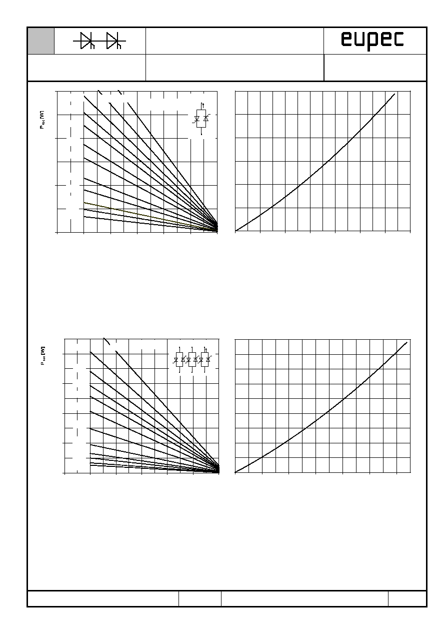
Durchgangsverluste bei Sinus
Durchgangsverluste bei Rechteck
0
100
200
300
400
500
600
700
800
0
100
200
300
400
500
600
I
TAV
[A]
P
TAV
[W
]
Q = 30į
60į
90į
120į
180į
0į
0
180į
Durchlassverlustleistung je Zweig / On-state power loss per arm P
TAV
= f(I
TAV
)
SinusfŲrmiger Strom / Sinusoidal current Strombelastung je Zweig / Current load per arm
Berechnungsgrundlage P
TAV
(Schaltverluste gesondert berŁcksichtigen)
Calculation base P
TAV
(switching losses should be considered separately)
Parameter: StromfluŖwinkel / Current conduction angle
0
200
400
600
800
1000
0
100
200
300
400
500
600
700
800
900
I
TAV
[A]
DC
180į
120į
90į
60į
Q = 30į
0į
0
180į
Durchlassverlustleistung je Zweig / On-state power loss per arm P
TAV
= f(I
TAV
)
RechteckfŲrmiger Strom / Rectangular current Strombelastung je Zweig / Current load per arm
Berechnungsgrundlage P
TAV
(Schaltverluste gesondert berŁcksichtigen)
Calculation base P
TAV
(switching losses should be considered separately)
Parameter: StromfluŖwinkel / Current conduction angle

N
Netz-Thyristor-Modul
Phase Control Thyristor
Module
Datenblatt / Data sheet
TT500N
BIP AC / 05.08.96 R.JŲrke
A 33/94
7/12
Seite/page
Gehšusetemperatur bei Sinus
Gehšusetemperatur bei Rechteck
20
40
60
80
100
120
140
0
100
200
300
400
500
600
I
TAVM
[A]
T
C
[į
C]
Q = 30į
60į
90į
120į
180į
0į
0
180į
HŲchstzulšssige Gehšusetemperatur / Maximum allowable case temperature T
C
= f(I
TAVM
)
SinusfŲrmiger Strom / Sinusoidal current Strombelastung je Zweig / Current load per arm
Berechnungsgrundlage P
TAV
(Schaltverluste gesondert berŁcksichtigen)
Calculation base P
TAV
(switching losses should be considered separately)
Parameter: StromfluŖwinkel / Current conduction angle
20
40
60
80
100
120
140
0
100
200
300
400
500
600
700
800
900
I
TAVM
[A]
Q = 30į
60į
90į
120į
180į
DC
0į
0
180į
HŲchstzulšssige Gehšusetemperatur / Maximum allowable case temperature T
C
= f(I
TAVM
)
RechteckfŲrmiger Strom / Rectangular current Strombelastung je Zweig / Current load per arm
Berechnungsgrundlage P
TAV
(Schaltverluste gesondert berŁcksichtigen)
Calculation base P
TAV
(switching losses should be considered separately)
Parameter: StromfluŖwinkel / Current conduction angle

N
Netz-Thyristor-Modul
Phase Control Thyristor
Module
Datenblatt / Data sheet
TT500N
BIP AC / 05.08.96 R.JŲrke
A 33/94
8/12
Seite/page
Maximaler Strom bei B2 und B6
0
500
1000
1500
2000
2500
3000
0
20
40
60
80
100
120
T
A
[įC]
R
thCA
[įC/W]
0,03
0,10
0,15
0,04
0,015
0,06
+
-
B2
I
D
~
0,01
0,02
0,08
0,20
0,30
0
200
400
600
800
1000
1200
I
D
[A]
L-Last
L-load
R-Last
R-load
HŲchstzulšssiger Ausgangsstrom / Maximum rated output current I
D
B2- Zweipuls-BrŁckenschaltung / Two-pulse bridge circuit
Gesamtverlustleistung der Schaltung / Total power dissipation at circuit P
tot
Parameter:
Wšrmewiderstand zwischen den Gehšusen und Umgebung / Thermal resistance cases to ambient R
thCA
0
1000
2000
3000
4000
0
20
40
60
80
100
120
T
A
[įC]
0,03
0,04
0,025
0,20
0,01
+
-
B6
I
D
3~
R
thCA
[įC/W]
0,15
0,40
0,015
0,10
0,06
,
0,02
0
200
400
600
800
1000
1200
1400
1600
I
D
[A]
HŲchstzulšssiger Ausgangsstrom / Maximum rated output current I
D
B6- Sechspuls-BrŁckenschaltung / Six-pulse bridge circuit
Gesamtverlustleistung der Schaltung / Total power dissipation at circuit P
tot
Parameter:
Wšrmewiderstand zwischen den Gehšusen und Umgebung / Thermal resistance cases to ambient R
thCA
N
Netz-Thyristor-Modul
Phase Control Thyristor
Module
Datenblatt / Data sheet
TT500N
BIP AC / 05.08.96 R.JŲrke
A 33/94
9/12
Seite/page
Maximaler Strom bei W1C und W3C
0
500
1000
1500
0
20
40
60
80
100
120
T
A
[įC]
R
thCA
[įC/W]
0,30
0,60
0,02
0,03
0,04
0,06
0,08
0,10
0,15
0,20
~
~
I
RMS
W
1C
0,40
0,05
0
200
400
600
800
1000
1200
1400
I
RMS
[A]
HŲchstzulšssiger Effektivstrom / Maximum rated RMS current I
RMS
W1C - Einphasen-Wechselwegschaltung / Single-phase inverse parallel circuit
Gesamtverlustleistung der Schaltung / Total power dissipation at circuit P
tot
Parameter:
Wšrmewiderstand zwischen den Gehšuse und Umgebung / Thermal resistance case to ambient R
thCA
0
1000
2000
3000
4000
0
20
40
60
80
100
120
T
A
[įC]
R
thCA
[įC/W]
0,15
0,20
0,025
0,03
0,01
0,04
0,015
0,10
~
~
W
3C
~
~
I
RMS
~
~
0,06
0,30
0,40
0,02
0
200
400
600
800
1000
1200
I
RMS
[A]
HŲchstzulšssiger Effektivstrom / Maximum rated RMS current I
RMS
W3C - Dreiphasen-Wechselwegschaltung / Three-phase inverse parallel circuit
Gesamtverlustleistung der Schaltung / Total power dissipation at circuit P
tot
Parameter:
Wšrmewiderstand zwischen den Gehšusen und Umgebung / Thermal resistance cases to ambient R
thCA

N
Netz-Thyristor-Modul
Phase Control Thyristor
Module
Datenblatt / Data sheet
TT500N
BIP AC / 05.08.96 R.JŲrke
A 33/94
10/12
Seite/page
Steuercharakteristik
ZŁndverzug
0,1
1
10
100
10
100
1000
10000
i
G
[mA]
a
b
c
Steuercharakteristik v
G
= f (i
G
) mit ZŁndbereichen fŁr V
D
= 6 V
Gate characteristic v
G
= f (i
G
) with triggering area for V
D
= 6 V
HŲchstzulšssige Spitzensteuerverlustleistung / Maximum rated
peak gate power dissipation P
GM
= f (t
g
) :
a - 20 W/10ms b - 40 W/1ms c - 60 W/0,5ms
0,1
1
10
100
1000
100
1000
10000
i
GM
[mA]
a
b
ZŁndverzug / Gate controlled delay time t
gd
= f(i
G
)
T
vj
= 25įC, di
G
/dt = i
GM
/1Ķs
a - maximaler Verlauf / Limiting characteristic
b - typischer Verlauf / Typical characteristic
N
Netz-Thyristor-Modul
Phase Control Thyristor
Module
Datenblatt / Data sheet
TT500N
BIP AC / 05.08.96 R.JŲrke
A 33/94
11/12
Seite/page
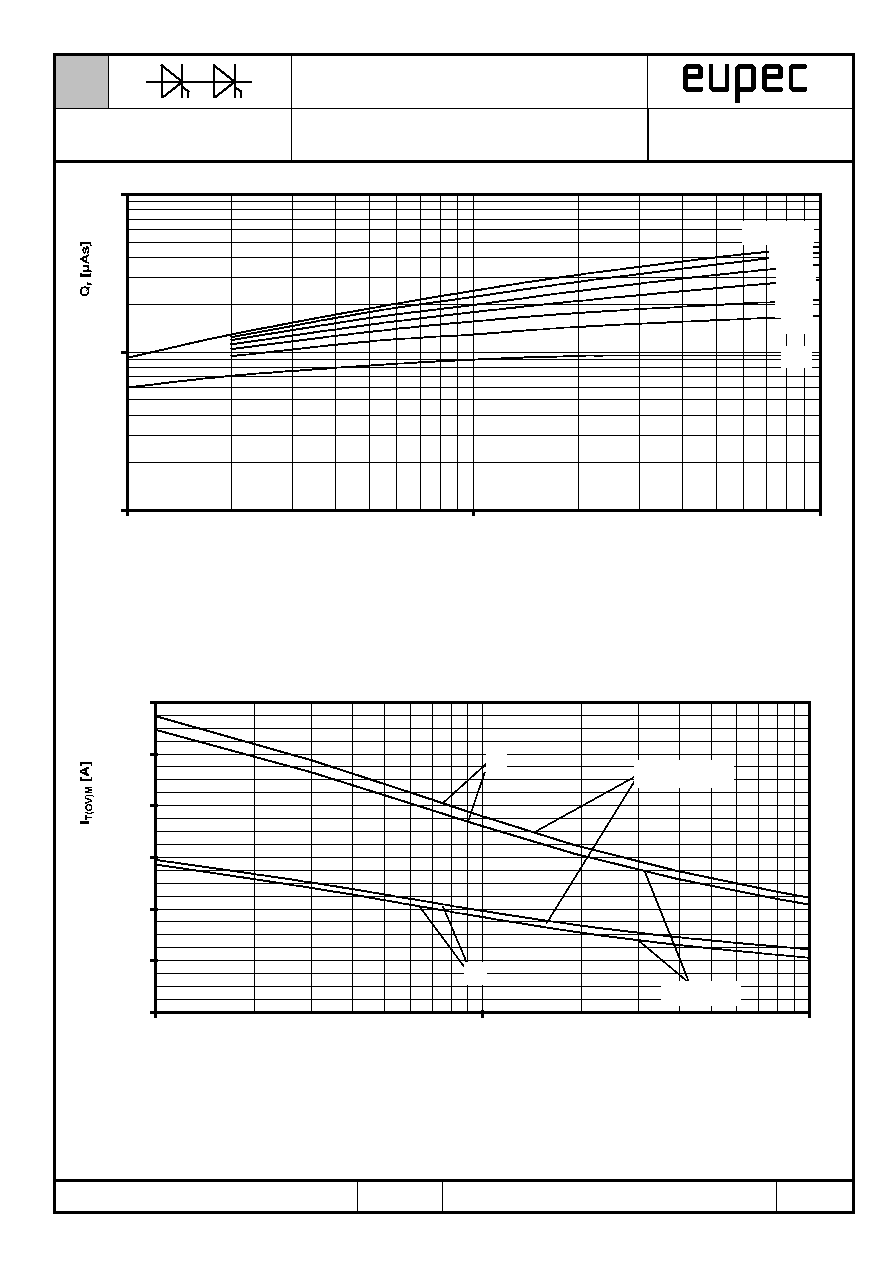
SperrverzŲgerungsladung
Grenzstrom
100
1000
10000
1
10
100
-di/dt [A/Ķs]
i
TM
= 2000A
20A
50A
100A
200A
500A
1000A
SperrverzŲgerungsladung / Recovered charge Q
r
= f(-di/dt)
T
vj
= T
vjmax
, v
R
0,5 V
RRM
, v
RM
= 0,8 V
RRM
Parameter: DurchlaŖstrom / On-state current i
TM
0
2.000
4.000
6.000
8.000
10.000
12.000
0,01
0,1
1
t [s]
b
T
A
= 45įC
a
T
A
= 35 įC
Grenzstrom / Maximum overload on-state current I
T(OV)M
= f(t), v
RM
= 0,8 V
RRM
a: Leerlauf / No-load conditions
b: nach Belastung mit I
TAVM
/ after load with I
TAVM
T
A
= 35įC, verstšrkte LuftkŁhlung / Forced air cooling
T
A
= 45įC, LuftselbstkŁhlung / Natural air cooling
N
Netz-Thyristor-Modul
Phase Control Thyristor
Module
Datenblatt / Data sheet
TT500N
BIP AC / 05.08.96 R.JŲrke
A 33/94
12/12
Seite/page
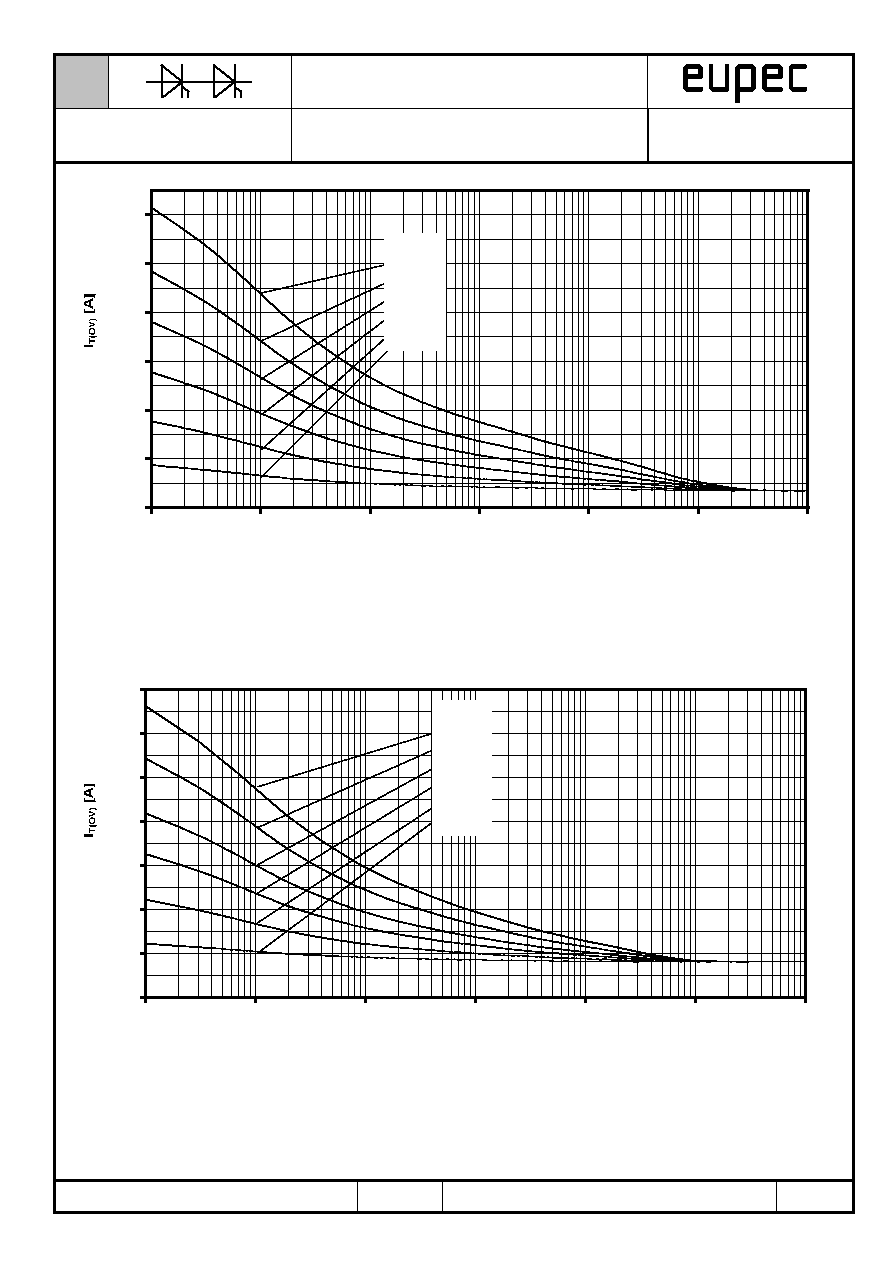
‹berstrom
0
1.000
2.000
3.000
4.000
5.000
6.000
0,01
0,1
1
10
100
1000
10000
t [s]
I
TAV (vor)
=
0 A
40 A
65 A
85 A
100 A
110 A
‹berstrom je Zweig / Overload on-state current I
T(OV)
B6- Sechspuls-BrŁckenschaltung, 120į Rechteck / Six-pulse bridge circuit, 120į rectangular
KŁhlkŲrper / Heatsink type KM 17 (120W) LuftselbstkŁhlung bei / Natural cooling at T
A
= 45įC
Parameter: Vorlaststrom je Zweig / Pre-load current per arm I
TAV(vor)
0
1.000
2.000
3.000
4.000
5.000
6.000
7.000
0,01
0,1
1
10
100
1000
10000
t [s]
I
TAV (vor)
=
0 A
90 A
160 A
200 A
235 A
260 A
‹berstrom je Zweig / Overload on-state current I
T(OV)
B6- Sechspuls-BrŁckenschaltung, 120į Rechteck / Six-pulse bridge circuit, 120į rectangular
KŁhlkŲrper / Heatsink type KM17 (Papst 4650N) Verstšrkte KŁhlung bei / Forced cooling at T
A
= 35įC
Parameter: Vorlaststrom je Zweig / Pre-load current per arm I
TAV(vor)