 | –≠–ª–µ–∫—Ç—Ä–æ–Ω–Ω—ã–π –∫–æ–º–ø–æ–Ω–µ–Ω—Ç: MP1231A | –°–∫–∞—á–∞—Ç—å:  PDF PDF  ZIP ZIP |
MP1230A/31A/32A
1
Rev. 2.00
FEATURES
∑
Superior Ruggedized 1230 Series: 2 KV ESD
∑
Four Quadrant Multiplication
∑
Stable, More Accurate Segmented DAC Approach
≠
0.2 ppm/
∞
C Linearity Tempco
≠
2 ppm/
∞
C Max Gain Error Tempco
≠
Lowest Sensitivity to Amplifier Offset
≠
Lowest Output Capacitance (C
OUT
= 80pF)
≠
Lower Glitch Energy
∑
Monotonic over Temperature Range
CMOS Microprocessor Compatible
Double-Buffered 12-Bit
Digital-to-Analog Converter
∑
Lower Data Bus Feedthrough @ CS = 1
∑
V
DD
from +11 V to +16 V
∑
Latch-Up Free CMOS Technology
∑
12-Bit Bus Version: MP1208/1209/1210
∑
16-Bit Upgrade: MP7636A
GENERAL DESCRIPTION
The MP1230A series are superior pin for pin replacements
for the 1230 series. The MP1230A series is manufactured using
advanced thin film resistors on a double metal CMOS process
which promotes significant improvements in reliability, latch-up
free performance and ESD protection.
The MP1230A series incorporates a unique decoding tech-
nique yielding lower glitch, higher speed and excellent accuracy
over temperature and time. 12-bit linearity is achieved without
trimming. Outstanding features include:
≠
Stability: integral and differential linearity tempcos are rated
at 0.2 ppm/
∞
C typical. Monotonicity is guaranteed over all
temperature ranges. Scale factor tempco is a low 2 ppm/
∞
C
maximum.
≠
Low Output Capacitance: Due to smaller MOSFET switch
geometries allowed by decoding, the output capacitance at
I
OUT1
and I
OUT2
is a low 80pF / 40pF and 25pF / 65 pF. This
less than half the competitive DAC 1230 series. Lower ca-
pacitance allows the MP1230A series to achieve settling
times faster than 1
µ
s for a 10 V step.
≠
Low Sensitivity to Output Amplifier Offset: The linearity er-
ror caused by amplifier offset is reduced by a factor of 2 in the
MP1230A series over conventional R-2R DACs.
The MP1230A series uses a circuit which reduces transients
in the supplies caused by DATA bus transitions at CS
= 1.
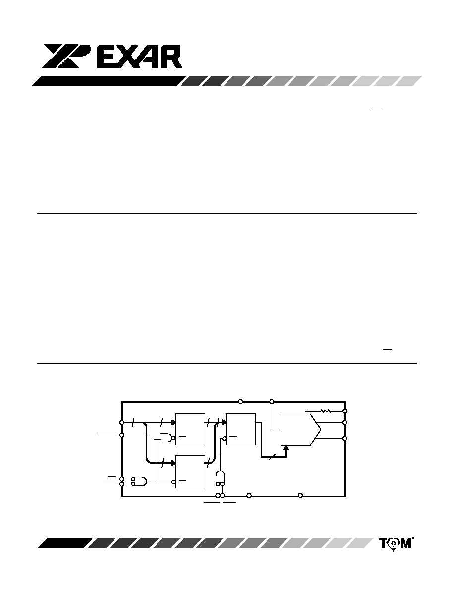
SIMPLIFIED BLOCK DIAGRAM
DGND
12
D
Q
D
Q
DB11-DB4
DB3-DB0
D
Q
AGND
12
8
4
4
8
8
INPUT LATCH
DAC LATCH
V
DD
V
REF
R
FB
I
OUT1
I
OUT2
V
REF
BYTE1/BYTE2
CS
WR1
XFER WR2
LE
LE
LE

MP1230A/31A/32A
2
Rev. 2.00
ORDERING INFORMATION
Package
Type
Temperature
Range
Part No.
Plastic Dip
Plastic Dip
Plastic Dip
≠40 to +85
∞
C
≠40 to +85
∞
C
≠40 to +85
∞
C
+1/2
+3/4
+1
+1
+2
+2
+0.4
+0.4
+0.4
MP1230ABN
MP1231ABN
MP1232ABN
SOIC
MP1230ABS
≠40 to +85
∞
C
SOIC
MP1231ABS
≠40 to +85
∞
C
SOIC
MP1232ABS
≠40 to +85
∞
C
+1/2
+3/4
+0.4
+1
+1
+0.4
+2
+2
+0.4
INL
(LSB)
DNL
(LSB)
Gain Error
(% FSR)
PIN CONFIGURATIONS
20 Pin PDIP (0.300")
N20
AGND
DGND
DB7
DB6
DB5
DB4
20
1
11
10
2
3
4
5
6
7
15
14
13
12
17
16
8
9
19
18
20 Pin SOIC (Jedec, 0.300")
S20
1
2
3
4
5
6
7
8
9
10
20
19
18
17
16
15
14
13
12
11
V
DD
I
OUT2
I
OUT1
R
FB
V
REF
DB8 (DB0, LSB)
DB9 (DB1)
DB10 (DB2)
DB11 MSB (DB3)
V
DD
I
OUT2
I
OUT1
DB8 (DB0, LSB)
DB9 (DB1)
DB10 (DB2)
DB11 MSB (DB3)
AGND
DGND
DB7
DB6
DB5
DB4
R
FB
V
REF
See Packaging Section for Package Dimensions
BYTE1/BYTE2
CS
WR1
XFER
WR2
BYTE1/BYTE2
XFER
WR2
CS
WR1
PIN OUT DEFINITIONS
1
CS
Chip Select (Active Low)
2
WR1
Write 1 (Active Low)
3
AGND
Analog Ground
4
DB7
Data Input Bit 7
5
DB6
Data Input Bit 6
6
DB5
Data Input Bit 5
7
DB4
Data Input Bit 4
8
V
REF
Reference Input Voltage
9
R
FB
Feedback Resistor
10
DGND
Digital Ground
11
I
OUT1
Current Output 1
PIN NO.
NAME
DESCRIPTION
12
I
OUT2
Current Output 2
13
DB11 (DB3)
Data Input Bit 11 (MSB)
Data Input Bit 3
14
DB10 (DB2)
Data Input Bit 10
Data Input Bit 2
15
DB9 (DB1)
Data Input Bit 9
Data Input Bit 1
16
DB8 (DB0)
Data Input Bit 8
Data Input Bit 0 (LSB)
17
XFER
Transfer Control Signal (Active Low)
18
WR2
Write 2 (Active Low)
19
BYTE1/
Byte Sequence Control
BYTE2
20
V
DD
Positive Power Supply
PIN NO.
NAME
DESCRIPTION
MP1230A/31A/32A
3
Rev. 2.00
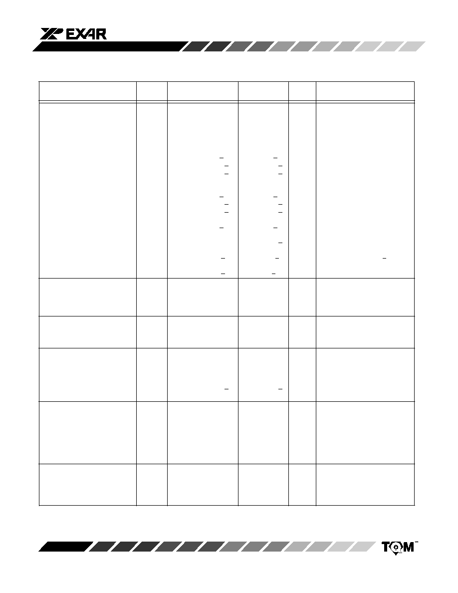
ELECTRICAL CHARACTERISTICS
(V
DD
= + 15 V, V
REF
= +10 V unless otherwise noted)
25
∞
C
Tmin to Tmax
Parameter
Symbol
Min
Typ
Max
Min
Max
Units
Test Conditions/Comments
STATIC PERFORMANCE
1
FSR = Full Scale Range
Resolution (All Grades)
N
12
12
Bits
Integral Non-Linearity
INL
LSB
Best Fit Straight Line Spec.
(Relative Accuracy)
(Max INL ≠ Min INL) / 2
MP1230ABN/ATD/ABS
+1/2
+1/2
MP1231ABN/ATD/ABS
+1
+1
MP1232ABN/ATD/ABS
+2
+2
Differential Non-Linearity
DNL
LSB
MP1230ABN/ATD/ABS
+3/4
+3/4
MP1231ABN/ATD/ABS
+1
+1
MP1232ABN/ATD/ABS
+2
+2
Gain Error
GE
+0.4
+0.4
% FSR
Using Internal R
FB
Gain Temperature Coefficient
2
TC
GE
0.5
+2
ppm/
∞
C
Gain/
Temperature
Power Supply Rejection Ratio
PSRR
5
+20
+20
ppm/%
|
Gain/
V
DD
|
V
DD
= + 0.25V
Output Leakage Current
I
OUT
1
+10
+200
nA
DYNAMIC PERFORMANCE
2
R
L
=100
, C
L
=13pF
Current Settling Time
t
S
1.0
µ
sec
Full Scale Change to 1/2 LSB
AC Feedthrough at I
OUT1
F
T
1.0
mV p-p
V
REF
=100kHz, 20Vp-p, sinewave
REFERENCE INPUT
Input Resistance
R
IN
5
10
20
5
20
k
DIGITAL INPUTS
Logical "1" Voltage
V
IH
3.0
2.4
3.0
V
Logical "0" Voltage
V
IL
0.8
0.8
V
Input Leakage Current
I
LKG
+1
+1
µ
A
V
IN
= 0, 5 V
Input Capacitance
2
10
pF
ANALOG OUTPUTS
2
Output Capacitance
C
OUT1
80
100
100
pF
DAC Inputs all 1's
C
OUT1
40
60
60
pF
DAC Inputs all 0's
C
OUT2
65
85
85
pF
DAC Inputs all 1's
C
OUT2
25
45
45
pF
DAC Inputs all 0's
POWER SUPPLY
Functional Voltage Range
4
V
DD
+4.5
+16
+4.5
+16
V
Supply Current
I
DD
1.2
2.0
2.0
mA
All digital inputs = 0 V or all = 5 V

MP1230A/31A/32A
4
Rev. 2.00
25
∞
C
NOTES:
Parameter
Symbol
Min
Typ
Max
Min
Max
Units
Test Conditions/Comments
SWITCHING
CHARACTERISTICS
2, 3
Chip Select to Write Set-Up Time
t
CS
200
100
ns
Chip Select to Write Hold Time
t
CH
10
0
ns
Data Valid to Write Set-Up Time
t
DS
100
50
ns
Data Valid to Write Hold Time
t
DH
90
70
ns
Write Pulse Width,
t
WR
100
50
ns
Specifications are subject to change without notice
ELECTRICAL CHARACTERISTICS (CONT'D)
Tmin to Tmax
1
Full Scale Range (FSR) is 10V.
2
Guaranteed but not production tested.
3
See timing diagram.
4
Specified values guarantee functionality. Refer to other parameters for accuracy.
ABSOLUTE MAXIMUM RATINGS (T
A
= +25
∞
C unless otherwise noted)
1, 2
V
DD
to GND
+17 V
. . . . . . . . . . . . . . . . . . . . . . . . . . . . . . . . . . .
Digital Input Voltage to GND
GND ≠0.5 to V
DD
+0.5 V
. . . .
I
OUT1
, I
OUT2
to GND
GND ≠0.5 to +6.5 V
. . . . . . . . . . . . . . . .
V
REF
to GND
+25 V
. . . . . . . . . . . . . . . . . . . . . . . . . . . . . . . . . .
V
RFB
to GND
+25 V
. . . . . . . . . . . . . . . . . . . . . . . . . . . . . . . . . .
AGND to DGND
+1 V
. . . . . . . . . . . . . . . . . . . . . . . . . . . . . . . . .
(Functionality Guaranteed +0.5 V)
Storage Temperature
≠65
∞
C to +150
∞
C
. . . . . . . . . . . . . . . . .
Lead Temperature (Soldering, 10 seconds)
+300
∞
C
. . . . . .
Package Power Dissipation Rating to 75
∞
C
CDIP, PDIP, SOIC
900mW
. . . . . . . . . . . . . . . . . . . . . . . . .
Derates above 75
∞
C
12mW/
∞
C
. . . . . . . . . . . . . . . . . . . . .
NOTES:
1
Stresses above those listed under "Absolute Maximum Ratings" may cause permanent damage to the device. This is a
stress rating only and functional operation at or above this specification is not implied. Exposure to maximum rating
conditions for extended periods may affect device reliability.
2
Any input pin which can see a value outside the absolute maximum ratings
should be protected by Schottky diode clamps
(HP5082-2835) from input pin to the supplies.
All inputs have protection diodes which will protect the device from short
transients outside the supplies of less than 100mA for less than 100
µ
s.
3
GND refers to AGND and DGND.

MP1230A/31A/32A
5
Rev. 2.00
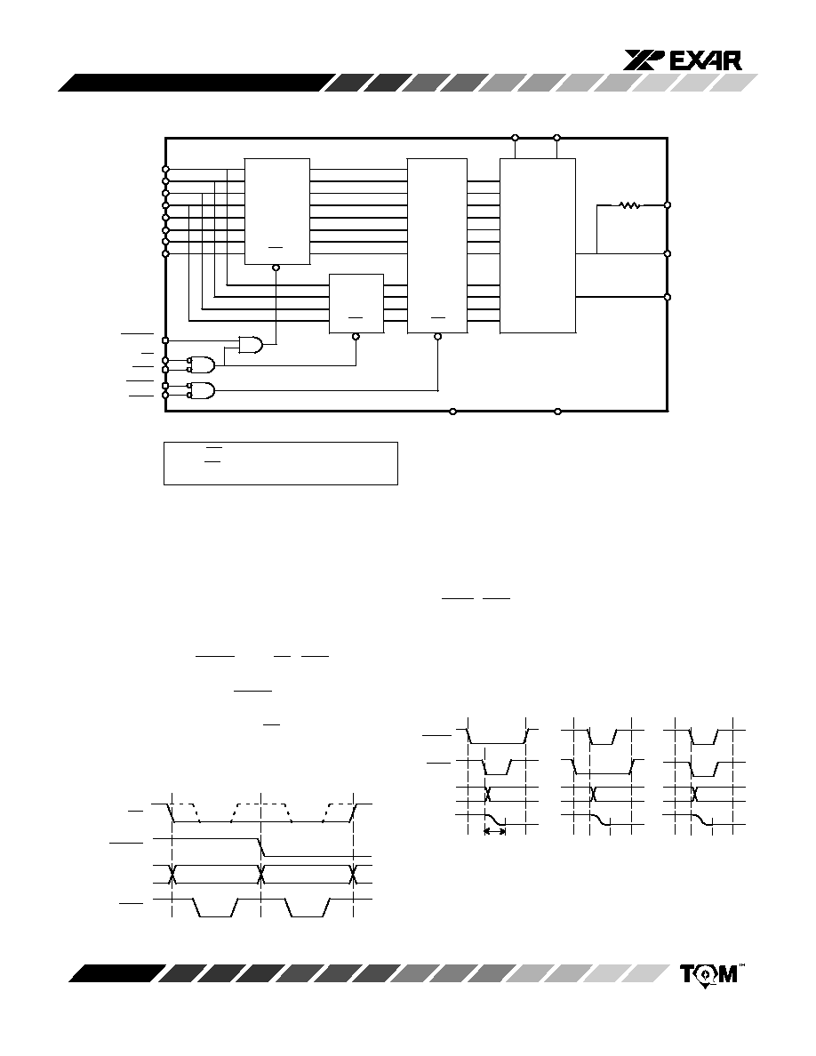
TIMING DIAGRAM
t
CH
50%
50%
50%
50%
50%
50%
SETTLED TO
+0.01%
CS, BYTE1/BYTE2
WR
DATA BITS
t
CS
t
WR
t
DS
t
DH
V
IH
V
IL
V
IH
V
IL
V
IH
V
IL
I
OUT1
, I
OUT2
t
S
DEFINITION OF CONTROL SIGNALS:
CS:
Chip Select.(Active low)
It will enable WR1.
WR1:
Write 1 (Active low)
The WR1 is used to load the digital data bits (DB) into
the input latch.
BYTE1/BYTE2:
Byte sequence control.
The BYTE1/BYTE2 control pin is used to select both
MSB and LSB input latches.
WR2:
Write 2 (Active low)
It will enable XFER.
XFER:
Transfer control signal (Active low)
This signal in combination with WR2 causes the 16-bit
data which is available in the input latches to transfer
to the DAC register
DB0 to DB11: Digital Inputs.
DB0 is the least significant digital input (LSB) and
DB11 is the most significant digital input (MSB).
I
OUT1
:
DAC Current Output 1 Bus.
I
OUT1
is a maximum for a digital code of all 1's in the
DAC register, and is zero for all 0's in the DAC register.
I
OUT2
:
DAC Current Output 2 Bus.
I
OUT2
is a complement of I
OUT1
.
R
FB
:
Feedback Resistor.
This internal feedback resistor should always be used
(not an external resistor) since it matches the resistors
in the DAC and tracks these resistors over tempera-
ture.
V
REF
:
Reference Voltage Input.
This input connects an external precision voltage
source to the internal DAC. The V
REF
can be selected
over the range of +25V to ≠25V or the analog signal for
a 4-quadrant multiplying mode application.
V
DD
:
Power Supply Voltage.
This is the power supply pin for the part. The V
DD
can
be from +5 V DC to +15 V DC, however optimum volt-
age is +12 to +15 V DC.
AGND: Analog Ground
Back gate of the DAC N-channel current steering
switches.
DGND: Digital Ground
MP1230A/31A/32A
6
Rev. 2.00
THEORY OF OPERATION
Figure 1. Functional Diagram
D
D
D
D
D
D
D
D
Q
Q
Q
Q
Q
Q
Q
Q
D
D
D
D
D
D
D
D
Q
Q
Q
Q
Q
Q
Q
Q
D
D
D
D
Q
Q
Q
Q
D
D
D
D
Q
Q
Q
Q
MSB
LSB
8-Bit
Input
Latch
4-Bit
Input
Latch
12-Bit
DAC
Register
12-Bit
Multiplying
D/A
Converter
BYTE1/BYTE2
CS
WR1
XFER
WR2
DGND
AGND
LE
LE
LE
When LE = 1, Q Outputs Follow D Inputs
When LE = 0, Q Outputs are Latched
V
DD
V
REF
R
FB
I
OUT1
I
OUT2
DB11 (MSB) (DB3)
DB10 (DB2)
DB9 (DB1)
DB8 (DB0)
DB7
DB6
DB5
DB4
Digital Interface
Figure 1. shows the internal control logic that controls the
writing of the input latches. It is easy to understand how the
MP1230A/31A/32A works by understanding each basic opera-
tion.
Writing to Input Latches
The condition BYTE1/BYTE2= high, CS = WR1 = 0 loads the
data bus DB11-DB4 into both input latches.
A second cycle with BYTE1/BYTE2 = low (
Figure 2.) loads
the pins DB11-DB8 (DB3-DB0) into the 4-bit input latch.
Timing diagrams show the inputs CS and DB11-DB0 to be
stable during the entire writing cycle. In reality all the above sig-
nals can change (
Figure 2.) as long as they meet the timing con-
ditions specified in the Electrical Characteristic Table.
Figure 2. Write Cycles to Input Latches
WR1
CS
BYTE1/BYTE2
DATA
Transferring Data to the DAC Latches
Once one or all the input latches have been loaded, the condi-
tion XFER= WR2= low transfers the content of the input latches
in the DAC latch. The outputs of the DAC latch change and the
DAC current (I
OUT
) will reach a new stable value within the set-
tling time t
S
(
Figure 3.).
WR2
XFER
DB11-0
t
S
Figure 3. Transfer Cycles from
Input Latches to DAC Latches
or
or
I
OUT

MP1230A/31A/32A
7
Rev. 2.00
PERFORMANCE CHARACTERISTICS
Graph 1. Relative Accuracy vs. Digital Code
APPLICATION NOTES
Refer to Section 8 for Applications Information
MP1230A/31A/32A
8
Rev. 2.00
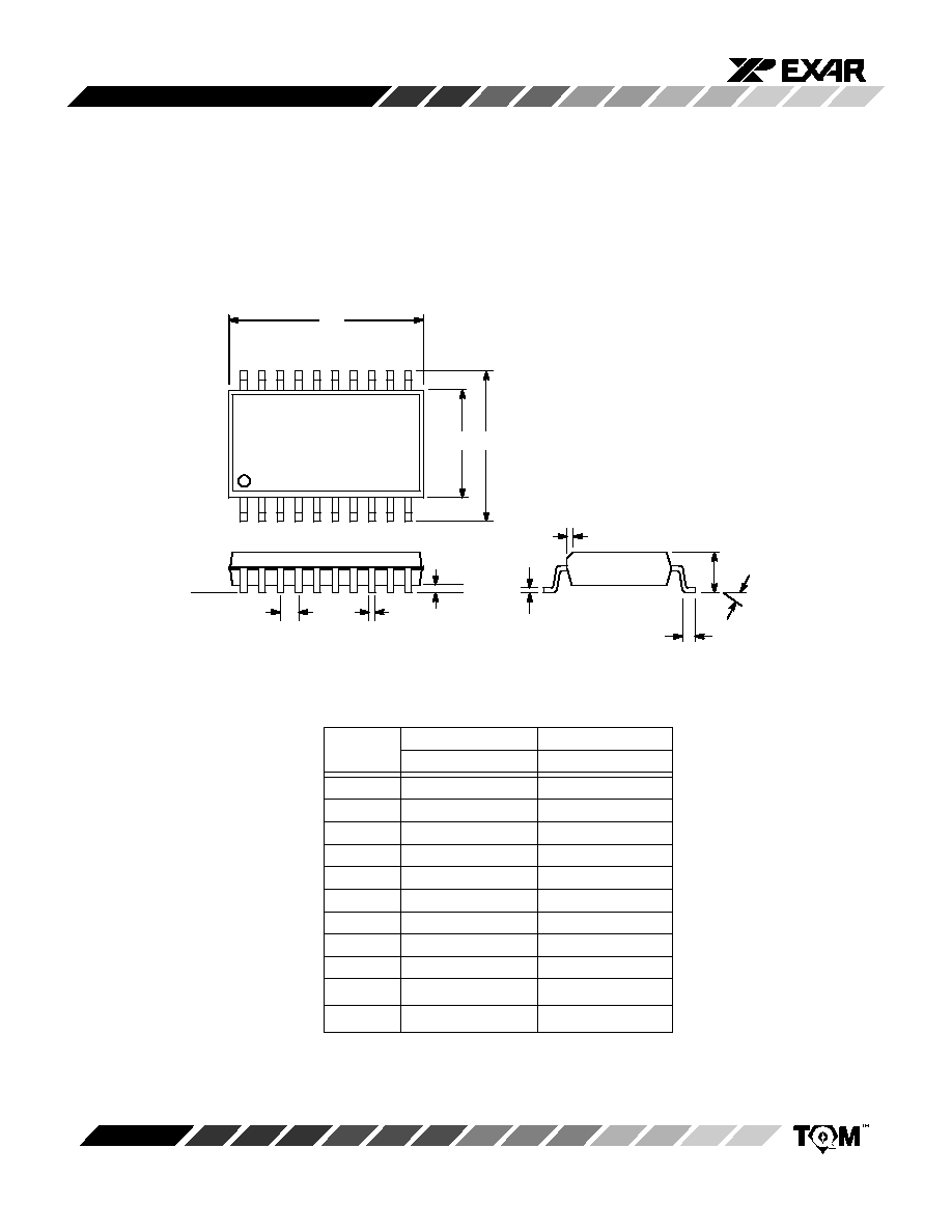
SYMBOL
MIN
MAX
MIN
MAX
A
0.097
0.104
2.464
2.642
A
1
0.0050
0.0115
0.127
0.292
B
0.014
0.019
0.356
0.483
C
0.0091
0.0125
0.231
0.318
D
0.500
0.510
12.70
12.95
E
0.292
0.299
7.42
7.59
e
0.050 BSC
1.27 BSC
H
0.400
0.410
10.16
10.41
h
0.010
0.016
0.254
0.406
L
0.016
0.035
0.406
0.889
0
∞
8
∞
0
∞
8
∞
INCHES
MILLIMETERS
e
20
11
20 LEAD SMALL OUTLINE
(300 MIL JEDEC SOIC)
S20
10
D
E
H
B
A
L
C
A
1
Seating
Plane
h x 45
∞

MP1230A/31A/32A
9
Rev. 2.00
20 LEAD PLASTIC DUAL-IN-LINE
(300 MIL PDIP)
N20
20
1
11
10
D
e
B
1
A
1
E
1
C
E
A
L
B
Q
1
Seating
Plane
SYMBOL
MIN
MAX
MIN
MAX
INCHES
A
≠≠
0.200
≠≠
5.08
A
1
0.015
≠≠
0.38
≠≠
B
0.014
0.023
0.356
0.584
B
1
(1)
0.038
0.065
0.965
1.65
C
0.008
0.015
0.203
0.381
D
0.945
1.060
24.0
26.92
E
0.295
0.325
7.49
8.26
E
1
0.220
0.310
5.59
7.87
e
0.100 BSC
2.54 BSC
L
0.115
0.150
2.92
3.81
0
∞
15
∞
0
∞
15
∞
Q
1
0.055
0.070
1.40
1.78
S
0.040
0.080
1.02
2.03
MILLIMETERS
S
Note:
(1)
The minimum limit for dimensions B1 may be 0.023"
(0.58 mm) for all four corner leads only.

MP1230A/31A/32A
10
Rev. 2.00
Notes

MP1230A/31A/32A
11
Rev. 2.00
Notes

MP1230A/31A/32A
12
Rev. 2.00
NOTICE
EXAR Corporation reserves the right to make changes to the products contained in this publication in order to im-
prove design, performance or reliability. EXAR Corporation assumes no responsibility for the use of any circuits de-
scribed herein, conveys no license under any patent or other right, and makes no representation that the circuits are
free of patent infringement. Charts and schedules contains here in are only for illustration purposes and may vary
depending upon a user's specific application. While the information in this publication has been carefully checked;
no responsibility, however, is assumed for inaccuracies.
EXAR Corporation does not recommend the use of any of its products in life support applications where the failure or
malfunction of the product can reasonably be expected to cause failure of the life support system or to significantly
affect its safety or effectiveness. Products are not authorized for use in such applications unless EXAR Corporation
receives, in writing, assurances to its satisfaction that: (a) the risk of injury or damage has been minimized; (b) the
user assumes all such risks; (c) potential liability of EXAR Corporation is adequately protected under the circum-
stances.
Copyright EXAR Corporation
Datasheet April 1995
Reproduction, in part or whole, without the prior written consent of EXAR Corporation is prohibited.