 | –≠–ª–µ–∫—Ç—Ä–æ–Ω–Ω—ã–π –∫–æ–º–ø–æ–Ω–µ–Ω—Ç: MP7226LN | –°–∫–∞—á–∞—Ç—å:  PDF PDF  ZIP ZIP |
MP7226
1
Rev. 2.00
FEATURES
∑
MPS Pioneered Segmented DAC Approach
∑
Four 8-Bit DACs with Buffer Amplifiers
∑
Bipolar Amplifier Inputs for Low Noise and Drift
∑
Operates with Single or Dual Supplies
∑ µ
P Compatible (95ns WR)
∑
No External Adjustments Required
∑
Power-on-Reset Function
∑
Specified for 5 to 15 V Operation
∑
ESD Protection: 2000 Volts Minimum
∑
Latch-Up Proof
∑
Octal Available: MP7228
BiCMOS
Fixed, Quad, Voltage Output, Single or Dual
Supply 8-Bit Digital-to-Analog Converter
APPLICATIONS
∑
Function Generators
∑
Automatic Test Equipment
∑
Process Controls
BENEFITS
∑
Reduced Board Space; Lower System Cost
∑
Reduced System Errors due to Excellent DAC-to-DAC
Matching and Tracking
∑
Easy to Design with Microprocessors
∑
Stable, High Reliability through Advanced Processing
∑
Lower 1/f Noise Increases Useful Dynamic Range
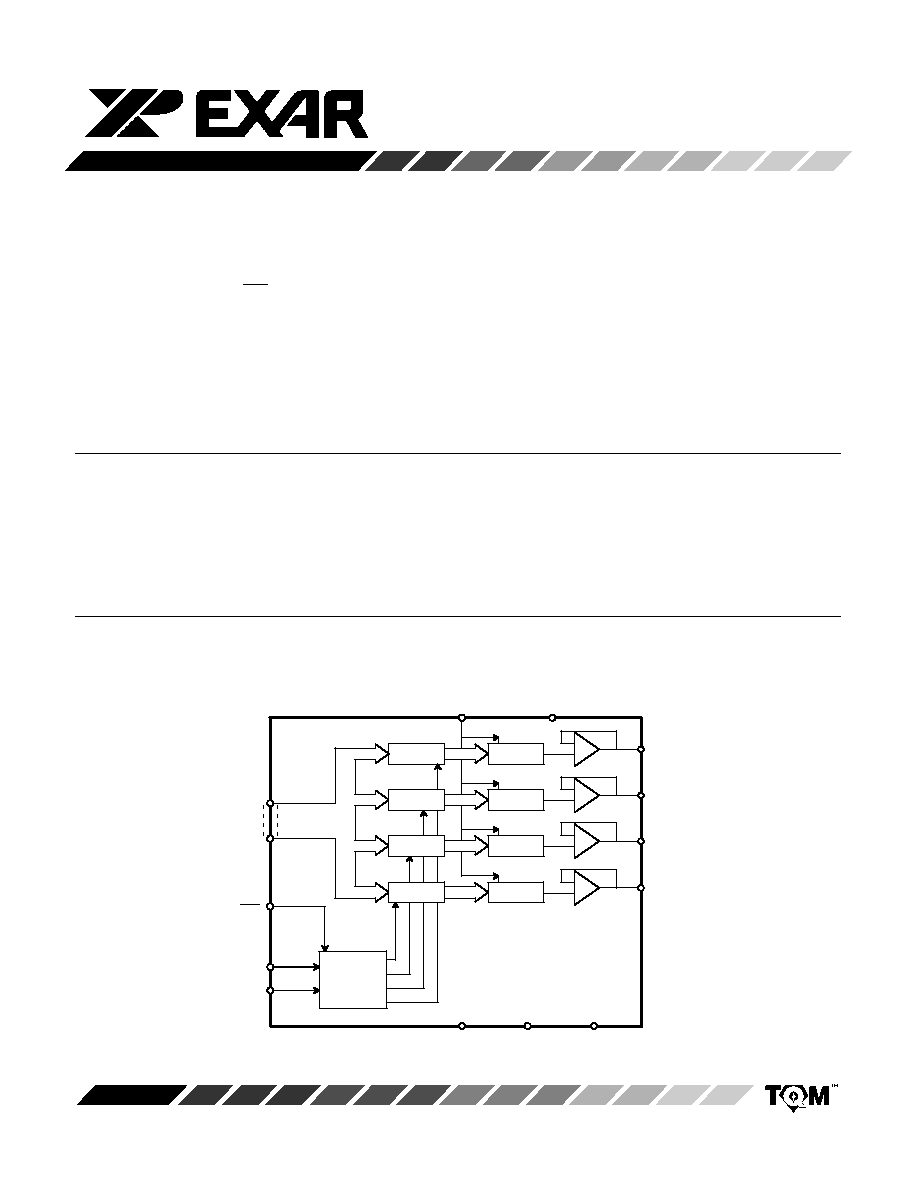
GENERAL DESCRIPTION
The MP7226 contains four 8-bit voltage-output Digital-to-
Analog Converters, with BiCMOS output buffer amplifiers and
interface logic on a monolithic chip. Separate on-chip latches
are provided for each of the four D/A converters. The control
logic is speed compatible with most 8-bit microprocessors. All
digital inputs are TTL/CMOS(5V) compatible.
The MP7226 is manufactured using advanced thin film resis-
tors on a double metal BiCMOS process. The MP7226 incorpo-
rates a unique bit decoding technique yielding lower glitch,
higher speed and excellent accuracy over temperature and
time. The MP7226 maintains 8-Bit accuracy over the full operat-
ing temperature range without laser trim or external adjust-
ments.
SIMPLIFIED BLOCK DIAGRAM
LATCH 1
DAC 1
≠
+
1
DAC 2
≠
+
2
DAC 3
≠
+
3
DAC 4
≠
+
4
V
OUT1
V
OUT2
V
OUT3
V
OUT4
V
REF
V
DD
LATCH 2
LATCH 3
LATCH 4
V
SS
AGND
MSB
LSB
DATA
(8 BIT)
WR
A1
A0
CONTROL
LOGIC
D
A
T
A
B
U
S
DGND
MP7226
2
Rev. 2.00
ORDERING INFORMATION
Package
Type
Temperature
Range
INL
(LSB)
Part No.
DNL
(LSB)
Full Scale
Error (LSB)
Plastic Dip
PLCC
SOIC
≠40 to +85
∞
C
MP7226KN
MP7226KP
MP7226KS
≠40 to +85
∞
C
≠40 to +85
∞
C
1
1
Plastic Dip
≠40 to +85
∞
C
MP7226LN*
1/2
PLCC
MP7226LP*
≠40 to +85
∞
C
SOIC
MP7226LS*
≠40 to +85
∞
C
*Contact factory for availability.
1
1/2
1
1/2
1/2
1/2
1/2
1/2
1/2
1/2
1/2
1
1/2
1
1/2
PIN CONFIGURATIONS
20 Pin PDIP (0.300")
N20
A0
A1
DB0 (LSB)
DB1
DB2
DB3
20 Pin SOIC (Jedec, 0.300")
S20
V
OUT2
V
OUT1
V
SS
V
REF
AGND
DGND
DB7 (MSB)
DB6
DB5
DB4
1
2
3
4
5
6
7
8
9
10
20
19
18
17
16
15
14
13
12
11
V
DD
V
OUT3
V
OUT4
20
1
11
10
2
3
4
5
6
7
15
14
13
12
17
16
8
9
19
18
See
Pin Out
at Left
3
2
1
20
19
9
10
11
12
13
4
5
6
7
8
18
17
16
15
14
See
Pin Out
at Far Left
20 Pin PLCC
P20
WR
See Packaging Section for Package Dimensions
PIN OUT DEFINITIONS
1
V
OUT2
DAC 2 Voltage Output
2
V
OUT1
DAC 1 Voltage Output
3
V
SS
Negative Power Supply (0 V to ≠5 V)
4
V
REF
Reference Input Voltage
5
AGND
Analog Ground
6
DGND
Digital Ground
7
DB7
Data Input Bit 7 (MSB)
8
DB6
Data Input Bit 6
9
DB5
Data Input Bit 5
10
DB4
Data Input Bit 4
PIN NO.
NAME
DESCRIPTION
11
DB3
Data Input Bit 3
12
DB2
Data Input Bit 2
13
DB1
Data Input Bit 1
14
DB0
Data Input Bit 0 (LSB)
15
WR
Write (Active Low)
16
A1
DAC Address Bit 1
17
A0
DAC Address Bit 0
18
V
DD
Positive Power Supply (+5 to +15 V)
19
V
OUT4
DAC 4 Voltage Output
20
V
OUT3
DAC 3 Voltage Output
PIN NO.
NAME
DESCRIPTION
MP7226
3
Rev. 2.00
ELECTRICAL CHARACTERISTICS
Single or Dual Supply Operation (V
DD
= +10.8 V to 16.5 V, V
SS
= 0 V or ≠5 V
10%, AGND = 0 V,
DGND = 0 V, V
REF
= +2 V to +10 V, R
L
= 2k
, C
L
= 100pF unless otherwise noted)
25
∞
C
Tmin to Tmax
Parameter
Symbol
Min
Typ
Max
Min
Max
Units
Test Conditions/Comments
STATIC PERFORMANCE
Resolution (All Grades)
N
8
8
Bits
Integral Non-Linearity
INL
LSB
(Relative Accuracy)
K
1
1
End Point Linearity Spec
L
1/2
1/2
Differential Non-Linearity
DNL
LSB
All grades monotonic over full
K
1/2
3/4
temperature range.
L
1/2
3/4
Total Unadjusted Error
2
LSB
V
DD
= 15 V
10%, V
REF
= +10 V
K
2
2
L
1
1
Full Scale Error
3
LSB
V
REF
= +10 V typ. Tempco is
K
1
1
5 ppm/
∞
C
L
1/2
1/2
Zero Code Error
mV
TA = 25
∞
C typ. Tempco is
K
20
30
30
µ
V/
∞
C
L
15
20
Output Load Resistance
2
2
k
V
OUT
= +10 V
DYNAMIC PERFORMANCE
4
Voltage Output Slew Rate
2
4
2
V/
µ
s
Voltage Output Settling Time
4
5
µ
s
V
REF
= +10 V; Settling Time to
1/2 LSB
Digital Feedthrough
25
nVs
Code transition all 0s to all 1s
V
REF
= 0 V, WR = V
DD
Digital Crosstalk
5
25
nVs
Code transition all 0s to all 1s
V
REF
= +10 V, WR = 0 V
REFERENCE INPUT
Reference Input Range
1
1
10
1
10
V
Limitation: V
REF
≠ V
SS
< 11 V
Reference Input Resistance
R
IN
2
2
k
Min R
IN
at Code 149
10
Reference Input Capacitance
4
500
pF
Occurs when all DACs are loaded
with all 1s
AC Feedthrough
≠70
dB
V
REF
= 10 kHz, 5 V p-p sinewave
DIGITAL INPUTS
Input High Voltage
V
INH
2.4
2.4
V
Input Low Voltage
V
INL
0.8
0.8
V
Input Leakage Current
I
LKG
1
1
µ
A
V
IN
= 0 V or V
DD
Input Capacitance
4
8
8
pF
Input Coding
Binary
MP7226
4
Rev. 2.00
ELECTRICAL CHARACTERISTICS (CONT'D)
25
∞
C
Tmin to Tmax
Parameter
Symbol
Min
Typ
Max
Min
Max
Units
Test Conditions/Comments
POWER SUPPLY
V
DD
Range
10.8
16.5
10.8
16.5
V
For specified performance
V
SS
Range (Dual Supplies)
8
0
≠5.5
0
≠5.5
V
For specified performance
I
DD
12
14
mA
Outputs unloaded;
V
IN
=V
INL
or V
INH
I
SS
(Dual Supplies)
10
12
Outputs unloaded;
V
IN
=V
INL
or V
INH
SWITCHING
CHARACTERISTICS
4, 6, 7
Address to WR Setup Time, t1
t
AS
0
0
ns
Address to WR Hold Time, t2
t
AH
0
0
ns
Data Valid to WR Setup Time, t3
t
DS
70
95
ns
Data Valid to WR Hold Time, t4
t
DH
10
10
WR Pulse Width, t5
t
WR
95
120
ns
NOTES:
Specifications are subject to change without notice
1
V
OUT
must be less than V
DD
by 3.5 V to ensure correct operation.
2
Total Unadjusted Error includes zero code error, relative accuracy and full-scale error.
3
Calculated after zero code error has been adjusted out.
4
Sample tested at 25
∞
C to ensure compliance.
5
The glitch impulse transferred to the output of one converter (not adjusted) due to a change in the digital input code to another
addressed converter.
6
All input rise and fall times are measured from 10% to 90% of +5 V, t
R
= t
F
= 5 ns.
7
Timing measurement reference level is (V
INH
+ V
INL
)/2.
MP7226
5
Rev. 2.00
ELECTRICAL CHARACTERISTICS
Single & Dual
5 V Supply Operation (V
DD
= +5 V
5%, V
SS
= 0 V to ≠5 V
10%, V
REF
= +1.25 V,
AGND = 0 V, DGND = 0 V, R
L
= 2k
, C
L
= 100pF unless otherwise noted)
25
∞
C
Tmin to Tmax
Parameter
Symbol
Min
Typ
Max
Min
Max
Units
Test Conditions/Comments
STATIC PERFORMANCE
Resolution (All Grades)
N
8
8
Bits
Integral Non-Linearity
INL
LSB
(Relative Accuracy)
K
2
2
End Point Linearity Spec
L
1
1
Differential Non-Linearity
DNL
LSB
All grades monotonic over full
K
1
1
temperature range.
L
1
1
Total Unadjusted Error
2
4
LSB
V
DD
= 5 V
5%, V
REF
= 1.25 V
Full Scale Error
3
LSB
V
REF
= +1.25 V
K
4
4
L
2
2
Zero Code Error
20
mV
Output Load Resistance
2
k
V
OUT
= +10 V
DYNAMIC PERFORMANCE
4
Voltage Output Slew Rate
2
4
V/
µ
s
Voltage Output Settling Time
4
µ
s
V
REF
= +1.25 V; Settling Time to
1/2 LSB
Digital Feedthrough
25
nVs
Code transition all 0s to all 1s
V
REF
= 0 V, WR = V
DD
Digital Crosstalk
5
25
nVs
Code transition all 0s to all 1s
V
REF
= +1.25 V, WR = 0 V
REFERENCE INPUT
Reference Input Range
1
1.6
1
1.6
V
V
OUT
must be < V
DD
by 3.2V
Reference Input Resistance
R
IN
2
2
k
Reference Input Capacitance
4
500
pF
Occurs when all DACs are loaded
with all 1s
AC Feedthrough
≠70
dB
V
REF
= 10 kHz, 1/2 V p-p sinewave
DIGITAL INPUTS
Input High Voltage
V
INH
2.4
2.4
V
Input Low Voltage
V
INL
0.8
0.8
V
Input Leakage Current
I
LKG
1
1
µ
A
V
IN
= 0 V or V
DD
Input Capacitance
4
8
8
pF
Input Coding
Binary
MP7226
6
Rev. 2.00
ELECTRICAL CHARACTERISTICS (CONT'D)
25
∞
C
Tmin to Tmax
Parameter
Symbol
Min
Typ
Max
Min
Max
Units
Test Conditions/Comments
POWER SUPPLY
V
DD
Range
4.75
5.25
4.75
5.25
V
For specified performance
I
DD
8
8
mA
Outputs unloaded;
V
IN
=V
INL
or V
INH
I
SS
(Dual Supplies)
6
6
Outputs unloaded;
V
IN
=V
INL
or V
INH
SWITCHING
CHARACTERISTICS
4, 6, 7
Address to WR Setup Time, t1
t
AS
0
0
ns
Address to WR Hold Time, t2
t
AH
0
0
ns
Data Valid to WR Setup Time, t3
t
DS
70
95
ns
Data Valid to WR Hold Time, t4
t
DH
0
WR Pulse Width, t5
t
WR
95
120
ns
NOTES:
Specifications are subject to change without notice
1
V
OUT
must be less than V
DD
by 3.5 V to ensure correct operation.
2
Total Unadjusted Error includes zero code error, relative accuracy and full-scale error.
3
Calculated after zero code error has been adjusted out.
4
Sample tested at 25
∞
C to ensure compliance.
5
The glitch impulse transferred to the output of one converter (not adjusted) due to a change in the digital input code to another
addressed converter.
6
All input rise and fall times are measured from 10% to 90% of +5 V, t
R
= t
F
= 5 ns.
7
Timing measurement reference level is (V
INH
+ V
INL
)/2.
ABSOLUTE MAXIMUM RATINGS (T
A
= +25
∞
C unless otherwise noted)
1, 2
V
DD
to AGND, DGND
0 to +17 V
. . . . . . . . . . . . . . . . . . . . . .
Digital Input Voltage to DGND
≠0.5 to V
DD
+0.5 V
. . . . . . . .
V
REF
to AGND, DGND
≠0.5 to V
DD
+0.5 V
. . . . . . . . . . . . . .
V
SS
to AGND, DGND
+0.5 to ≠7 V
. . . . . . . . . . . . . . . . . . . . .
AGND to DGND
+1 V
. . . . . . . . . . . . . . . . . . . . . . . . . . . . . . . . .
(Functionality Guaranteed +0.5 V)
Storage Temperature
≠65
∞
C to +150
∞
C
. . . . . . . . . . . . . . . . .
Lead Temperature (Soldering, 10 seconds)
+300
∞
C
. . . . . .
Package Power Dissipation Rating to 75
∞
C
PDIP, SOIC, PLCC
900mW
. . . . . . . . . . . . . . . . . . . . . . . .
Derates above 75
∞
C
12mW/
∞
C
. . . . . . . . . . . . . . . . . . . . .
NOTES:
1
Stresses above those listed under "Absolute Maximum Ratings" may cause permanent damage to the device. This is a
stress rating only and functional operation at or above this specification is not implied. Exposure to maximum rating
conditions for extended periods may affect device reliability.
2
Any input pin which can see a value outside the absolute maximum ratings
should be protected by Schottky diode clamps
(HP5082-2835) from input pin to the supplies.
All inputs have protection diodes which will protect the device from short
transients outside the supplies of less than 100mA for less than 100
µ
s.

MP7226
7
Rev. 2.00
D/A CONVERTER SECTION
The MP7226 contains four matched, 8-bit, voltage-mode Dig-
ital-to-Analog Converters (DACs) which incorporate an MPS
pioneered unique bit decoding technique. This decoding
scheme reduces the maximum binary weight carried by any re-
sistor switch, reducing the accuracy required of the switches
and resistor network.
In the MP7226, the first three MSBs are decoded into three
equal current sources, each contributing 25% of the full scale
output current.
Decoding two bits to three, a 1% change in any one of the
converter's three decoded current sources affects the output by
no more than 0.25% of full scale, compared with 0.5% in a con-
ventional R-2R type CMOS DAC.
The output voltages have the same polarity as the reference
voltage, allowing single supply operation. The voltage refer-
ence range is from +2V to +10V. Each DAC uses a highly-stable,
thin-film, ladder network and high-speed NMOS switches.
Figure 1. shows a simplified circuit diagram for one channel.
2R
4R
4R
4R
4R
2R
2R
Switch Drivers
Figure 1. Simplified D/A Circuit Diagram
≠
+
2 to 3 Decoder
4R
4R
V
REF
AGND
Shown for all 1s on DAC
V
OUT
V
REF
Input
The V
REF
and AGND are common to all four DACs and set
the full-scale output. The input impedance of the V
REF
pin is the
parallel combination of the four individual DAC reference imped-
ances and is code dependent. This impedance varies from 2k
to 500k
. Therefore, it is very important that the external refer-
ence source output impedance is low enough so that its output
voltage will not be affected by the varying digital code. Due to
transient currents at the V
REF
input during digital code changes,
a 0.1
µ
F or greater decoupling capacitor on that V
REF
input is
recommended. The input capacitance at the V
REF
pin is also
code dependent and typically varies from less than 120pF to
350pF.
Each V
OUT
voltage can be represented by a digitally pro-
grammable voltage source using the following expression :
V
OUT
= Dn X V
REF
/256
where Dn is the decimal equivalent to the digital input code
and can vary from 0 to 255.
Output Buffer Amp
Each D/A converter output is buffered by a unity gain nonin-
verting BiCMOS amplifier which has slew rate greater than 2 V/
µ
s . The output buffer settles to
1/2 LSB in less than 4
µ
s when
driving a load of 2k
in parallel with 100pF with a full scale transi-
tion from 0V to +10V or from +10V to 0V . The buffers can drive
2k
and 500pF to 10V levels without oscillation.
A simplified circuit diagram of the output buffer is shown in
Figure 2. The Input stage is provided by BiCMOS PNP transis-
tors with resulting lower input offset voltage, offset voltage drift
over time and noise when compared to MOS process . The am-
plifier output stage uses a substrate NPN bipolar device to pro-
vide a low output impedance, high-output current capability.
The MP7226 is specified for single or dual power supply op-
eration, with only the buffer amplifier outputs using V
SS
supply
current . Operating the MP7226 from dual supplies will improve
the negative going output settling time near ground. In dual sup-
ply voltage operation , the output amplifier can sink 500
µ
A when
V
OUT
= 0 V.
MP7226
8
Rev. 2.00
Figure 2. Simplified Output Buffer Amplifiers
V
DD
V
IN
AGND
V
SS
Output
The amplifiers outputs may be shorted to ground. However,
the power dissipation of the package should not exceed the
maximum limit.
Digital Inputs
All of the digital inputs to this DAC maintain TTL level inter-
face compatibility and can also be driven directly with 5V CMOS
logic inputs. The digital inputs are ESD protected to a rating of
2000 volts.
Digital Interface Logic
The MP7226 allows direct interface to most microprocessor
buses without additional interface circuitry.
Figure 3. shows the input control logic circuit diagram and
Table 1. shows the control logic truth table and operation for
WR, A1, A0. The address lines A0, and A1 determine which
DAC will accept the input data. The WR input determines
whether the selected DAC is transparent (output follows the in-
put), latched, or no operation. The WR input will also inhibit
power on reset of the DAC latches to 0, if its initial state = 0 after 5
µ
s of power.
Figure 4. shows the write cycle timing diagram. When the WR
signal is low, the input latch of the selected DAC is transparent,
and the DAC's output corresponds to the value present on the
data bus. On some data buses, data is not always valid for the
entire period that the WR signal is low and can cause unwanted
data at the output. Ensuring that the write pulse (WR) conforms
to the data hold time, (t4) spec will prevent this problem.
Figure 3. Input Control Logic
WR
To DAC1 Latch Enable
To DAC2 Latch Enable
To DAC3 Latch Enable
To DAC4 Latch Enable
A0
A1
1 of 4
Decoder
H
L
L
L
L
X
L
L
L
H
H
X
L
L
H
L
H
WR
A1
A0
Operation
No Operation;
Device Not Selected
DAC 1 Transparent
DAC 1 Latched
DAC 2 Transparent
DAC 3 Transparent
DAC 4 Transparent
Table 1. Truth Table
Figure 4. Write Cycle Timing Diagram
Address
Data
WR
t
AS
t
AH
t
WR
t
DS
t
DH
V
INH
V
INL
5 V
0 V
5 V
0 V
5 V
0 V
NOTE: When the WR signal is low, the input latch of the se-
lected DAC is transparent and any invalid data at this time will
cause erroneous output.
MP7226
9
Rev. 2.00
APPLICATIONS INFORMATION
Power On Reset
At power up, all inputs are reset to 0 V if WR = 1. For WR = 0,
the addressed DAC will receive input data.
Power Supply
The MP7226 can operate with either a single or dual power
supply. Improved zero-code settling error can be obtained by
using dual power supplies. The dual power supply specifica-
tions are a positive supply (V
DD
) range of +10.5V to +16.5V, and
a ≠5V supply (V
SS
) . The single power supply specifications are
a positive supply (V
DD
) range of +10.5V to +16.5V, or range of
+4.75V to 5.5V . The specified reference voltage (V
REF
) range
under these conditions is from +2V to V
DD
≠4V. For those appli-
cations requiring +10V at the output (V
REF
= +10V), V
DD
must
be +14V minimum to meet data sheet limits . 8-bit performance
is guaranteed for single supply operation (V
SS
= 0V); however,
zero code output sink capability is improved with V
SS
= ≠5V. For
adequate DAC and Buffer operation, V
REF
must always be be-
low V
DD
by at least 3.5V.
Power Supply Decoupling
The Power Supplies used with the MP7226 should be well
regulated and filtered. Local power supply decoupling consist-
ing of a 10
µ
F tantalum capacitor in parallel with a 0.01
µ
F ce-
ramic is recommended. The decoupling capacitors should be
connected between the V
DD
and AGND, and between V
SS
and
AGND if V
SS
= ≠5V.
Unipolar Output Operation
In this configuration, the reference voltage is the same polar-
ity as the output voltage. Since the reference voltage must al-
ways be positive with respect to GND, the output can only be 0 or
positive.
Table 2. shows the code relationship for the part in unipolar
operation
Table 2. Unipolar Code Table
1
1
1
0
0
0
1
0
0
1
0
0
1
0
0
1
0
0
1
0
0
1
0
0
1
0
0
1
0
0
1
0
0
1
0
0
1
0
0
1
0
0
1
1
0
1
1
0
Digital Input
Analog Output, V
OUT
) V
REF
(255
256)
) V
REF
(129
256)
) V
REF
(128
256) + )
V
REF
2
) V
REF
(127
256)
) V
REF
( 1
256)
0 V
Note : 1 LSB + (2
*8
) (V
REF
) + 1
256 (V
REF
)
Table 3. Bipolar Code Table
1
1
1
0
0
0
1
0
0
1
0
0
1
0
0
1
0
0
1
0
0
1
0
0
1
0
0
1
0
0
1
0
0
1
0
0
1
0
0
1
0
0
1
1
0
1
1
0
Digital Input
Analog Output
) V
REF
( 1
128)
* V
REF
( 1
128)
* V
REF
(127
128)
0 V
) V
REF
(127
128)
* V
REF
(128
128) + * V
REF
MP7226
10
Rev. 2.00
V
REF
V
REF
V
OUT
V
SS
AGND
DAC
≠
+
V
OUT
R2
R1
V
OUT
= D
n
X V
REF
X (1+R2/R1) ≠ V
REF
X R2/R1
if R1 = R2
V
OUT
= V
REF
X (2D
n
≠ 1)
Where D
n
is the digital input code and can vary from 0 to 255
Figure 5. Bipolar Output Circuit
≠
+
Bipolar Binary Operation
The Bipolar Mode configuration for each DAC requires one
external op-amp and two resistors per channel.
Figure 5. shows a typical Bipolar Operation circuit using the
MP7226.
Table 3. shows the code relationship for the circuit of
Figure 5. assuming R1 = R2 .
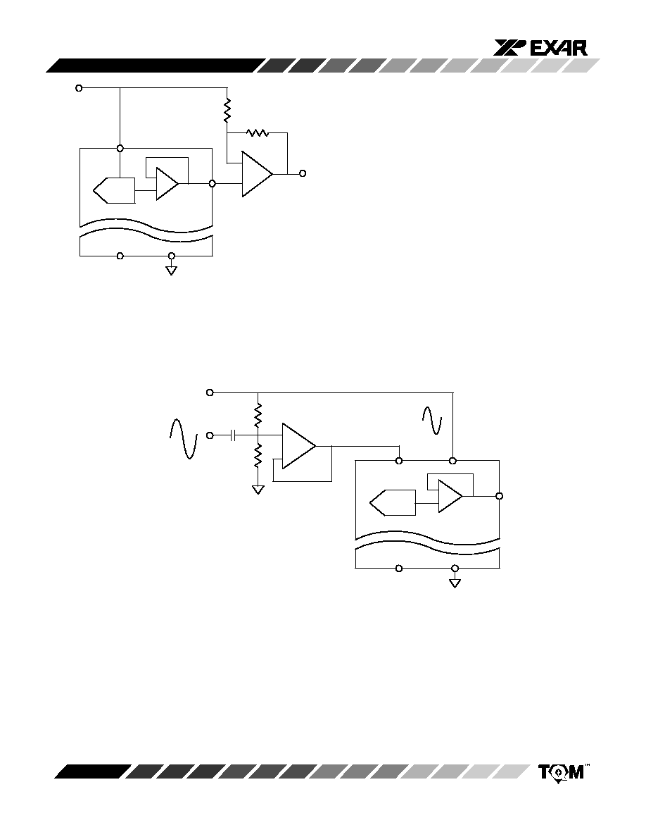
AC Reference Signal
An AC signal can be applied to the reference of the MP7226
for multiplying capability within the upper (+10V) and lower
(+2V) limits of the reference voltage input, with either single or
dual supplies . This signal must be level shifted or AC coupled
with proper bias level before being applied to the reference in-
put.
Figure 6. shows techniques for applying an AC signal to the
MP7226. Since all four DACs share a common reference, they
will all share this AC modulated reference. Input frequencies up
to 50kHz will typically be distorted less than 0.1% .
V
REF
V
DD
V
OUT
≠5 V or GND
AGND
DAC
≠
+
R1
Figure 6. AC Reference Input Signal Circuit (AC Couple)
≠
+
R2
C
AC
Reference
Input
+4 V
≠4 V
+15 V
DC
Offset
+10 V
+2 V
DC
OFFSET
= V
DD
(+15) X R2/R1+R2
V
SS

MP7226
11
Rev. 2.00
≠
+
Figure 7. Digitally Programmable Offset Adjustment Circuits
DAC
Output
V
OFFSET
V
OUT
V
OUT
= D
n
X V
REF
+ V
OFFSET
where D
n
is the digital input code
and can vary 0 to 255
≠
+
DAC
Output1
V
OUT
V
OUT
= D
n1
X V
REF
+ D
n2
X V
REF
where D
n
is the digital input code and
can vary 0 to 255
DAC
Output2
R
R
R
R
R
R
R
R
V
REF
V
DD
V
OUT
≠5 V or GND
AGND
DAC
≠
+
Figure 8. Digitally Programmable
AC Reference Input Signal Circuit (DC Couple)
≠
+
AC
Reference
Input
DAC
or DC Voltage
+15 V
V
SS
Offsetting DAC Outputs
Figure 7. shows examples of offset circuits.
DAC offset effects
When using the device in single supply applications, and
minimum reference voltage, there is a possibility that the DAC
output will not change when the code is incremented from 0.
Once the DAC has reached the offset voltage of the output
buffer, the DAC output will begin to increment in a normal opera-
tion.
5V Operation
The MP7226 can be operated with a single power supply
(V
DD
= +5V ) or dual power supplies ( V
DD
= +5V and V
SS
=
≠5V) . The reference voltage range is reduced along with Some
performance parameter degradation. However the DNL of each
DAC remains at
1 LSB guaranteeing monotonicity.
MP7226
12
Rev. 2.00
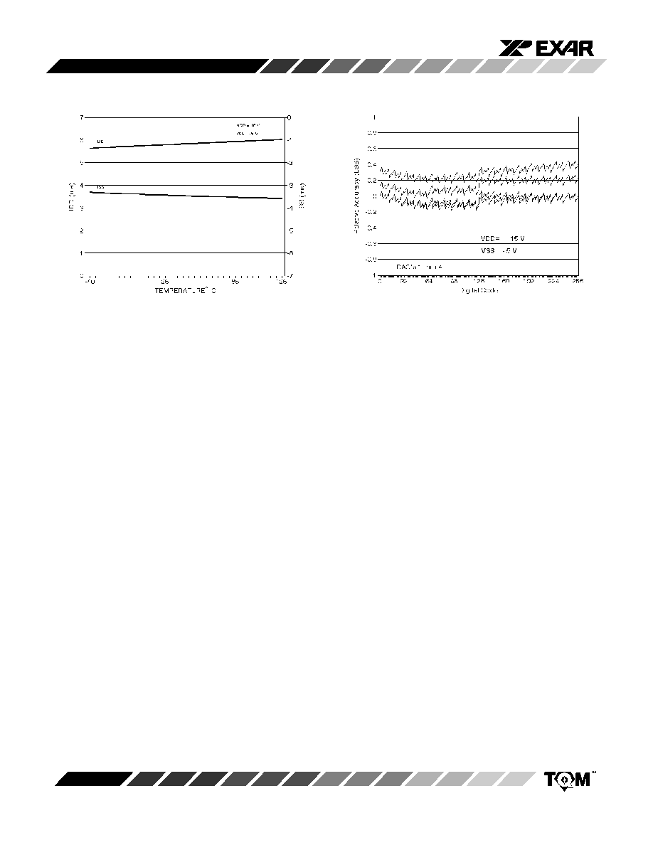
PERFORMANCE CHARACTERISTICS
Graph 1. Power Supply Current
vs. Temperature
Graph 2. Relative Accuracy
vs. Digital Code

MP7226
13
Rev. 2.00
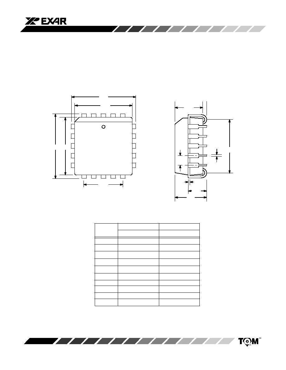
20 LEAD PLASTIC DUAL-IN-LINE
(300 MIL PDIP)
N20
20
1
11
10
D
e
B
1
A
1
E
1
C
E
A
L
B
Q
1
Seating
Plane
SYMBOL
MIN
MAX
MIN
MAX
INCHES
A
≠≠
0.200
≠≠
5.08
A
1
0.015
≠≠
0.38
≠≠
B
0.014
0.023
0.356
0.584
B
1
(1)
0.038
0.065
0.965
1.65
C
0.008
0.015
0.203
0.381
D
0.945
1.060
24.0
26.92
E
0.295
0.325
7.49
8.26
E
1
0.220
0.310
5.59
7.87
e
0.100 BSC
2.54 BSC
L
0.115
0.150
2.92
3.81
0
∞
15
∞
0
∞
15
∞
Q
1
0.055
0.070
1.40
1.78
S
0.040
0.080
1.02
2.03
MILLIMETERS
S
Note:
(1)
The minimum limit for dimensions B1 may be 0.023"
(0.58 mm) for all four corner leads only.

MP7226
14
Rev. 2.00
SYMBOL
MIN
MAX
MIN
MAX
A
0.097
0.104
2.464
2.642
A
1
0.0050
0.0115
0.127
0.292
B
0.014
0.019
0.356
0.483
C
0.0091
0.0125
0.231
0.318
D
0.500
0.510
12.70
12.95
E
0.292
0.299
7.42
7.59
e
0.050 BSC
1.27 BSC
H
0.400
0.410
10.16
10.41
h
0.010
0.016
0.254
0.406
L
0.016
0.035
0.406
0.889
0
∞
8
∞
0
∞
8
∞
INCHES
MILLIMETERS
e
20
11
20 LEAD SMALL OUTLINE
(300 MIL JEDEC SOIC)
S20
10
D
E
H
B
A
L
C
A
1
Seating
Plane
h x 45
∞
MP7226
15
Rev. 2.00
A
0.165
0.180
4.19
4.57
A
1
0.100
0.110
2.54
2.79
A
2
0.148
0.156
3.76
3.96
B
0.013
0.021
0.330
0.533
C
0.008
0.012
0.203
0.305
D
0.385
0.395
9.78
10.03
D
1
(1)
0.350
0.354
8.89
8.99
D
2
0.290
0.330
7.37
8.38
D
3
0.200 Ref
5.08 Ref.
e
1
0.050 BSC
1.27 BSC
20 LEAD PLASTIC LEADED CHIP CARRIER
(PLCC)
P20
SYMBOL
MIN
MAX
MIN
MAX
INCHES
MILLIMETERS
1
D
D
1
D
2
B
e
1
A
A
1
C
D
D
1
Seating
Plane
D
3
Note:
(1)
Dimension D
1
does not include mold protrusion.
Allowed mold protrusion is 0.254 mm/0.010 in.
A
2

MP7226
16
Rev. 2.00
NOTICE
EXAR Corporation reserves the right to make changes to the products contained in this publication in order to im-
prove design, performance or reliability. EXAR Corporation assumes no responsibility for the use of any circuits de-
scribed herein, conveys no license under any patent or other right, and makes no representation that the circuits are
free of patent infringement. Charts and schedules contains here in are only for illustration purposes and may vary
depending upon a user's specific application. While the information in this publication has been carefully checked;
no responsibility, however, is assumed for inaccuracies.
EXAR Corporation does not recommend the use of any of its products in life support applications where the failure or
malfunction of the product can reasonably be expected to cause failure of the life support system or to significantly
affect its safety or effectiveness. Products are not authorized for use in such applications unless EXAR Corporation
receives, in writing, assurances to its satisfaction that: (a) the risk of injury or damage has been minimized; (b) the
user assumes all such risks; (c) potential liability of EXAR Corporation is adequately protected under the circum-
stances.
Copyright 1993 EXAR Corporation
Datasheet April 1995
Reproduction, in part or whole, without the prior written consent of EXAR Corporation is prohibited.