 | –≠–ª–µ–∫—Ç—Ä–æ–Ω–Ω—ã–π –∫–æ–º–ø–æ–Ω–µ–Ω—Ç: MP7523JN | –°–∫–∞—á–∞—Ç—å:  PDF PDF  ZIP ZIP |
MP7523/XRD7523
Rev. 3.00
E
1996
EXAR Corporation, 48720 Kato Road, Fremont, CA 94538
z
(510) 668-7000
z
(510) 668-7010
FEATURES
∑
Full Four-Quadrant Multiplying
∑
Low Feedthrough: 1/2 LSB @ 200 kHz
∑
Fast Settling: 100 ns (typ.)
∑
Low Power Dissipation
∑
Low Cost
∑
5 V/15 V Operation
∑
Buffered Version: MP7524/XRD7524
15 V CMOS
Multiplying 8-Bit
Digital-to-Analog Converter
APPLICATIONS
∑
Battery Operated Equipment
∑
Low Power, Ratiometric A/D Converters
∑
Digitally Controlled Gain Circuits
∑
Digitally Controlled Attenuators
∑
CRT Character Generation
∑
Low Noise Audio Gain Control
...the analog plus company
TM
January 1996-2
GENERAL DESCRIPTION
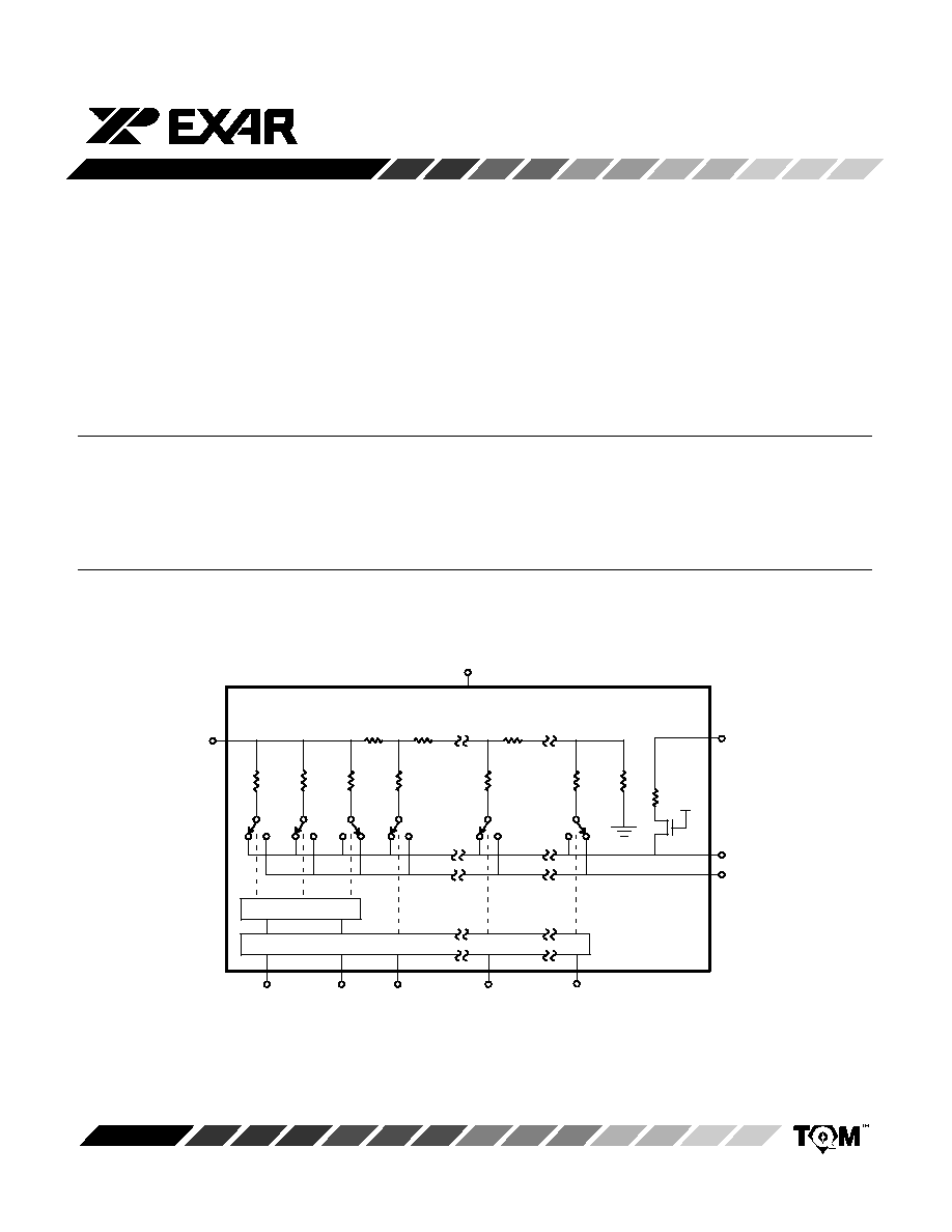
The MP7523/XRD7523 is a low cost multiplying Digital-to-
Analog Converter. The device uses an advanced thin-film-on-
CMOS technology to provide 8-bit resolution with accuracy to
10-bits and very low power dissipation.
The MP7523/XRD7523's excellent multiplying characteris-
tics and low cost allow it to be used in a wide ranging field of ap-
plications such as: low noise audio gain control, CRT character
generation, motor speed control, digitally controlled attenuators,
etc.
SIMPLIFIED BLOCK DIAGRAM
4R
R
2R
2 to 3 Decoder
MSB
LSB
4R
4R
4R
4R
4R
4R
2R
2R
Switch Drivers & Switches
3 Segment D/A Converter with Termination to DGND
Logical "1" at Digital Input Steers Current to I
OUT1
BIT 8
R = 10k
BIT 1
R
FB
I
OUT1
I
OUT2
V
REF
V
DD
MP7523/XRD7523
2
Rev. 3.00
ORDERING INFORMATION
Package
Type
Temperature
Range
Part No.
1/2
1/4
1/2
1/4
1.8
1.8
1.8
1.8
≠40 to +85
∞
C
≠40 to +85
∞
C
≠40 to +85
∞
C
≠40 to +85
∞
C
1
1
1
1
INL
(LSB)
Gain Error
(% FSR)
DNL
(LSB)
SOP (EIAJ)
XRD7523AIK-J
SOP (EIAJ)
XRD7523AIK-K
SOIC (Jedec, 0.150")
XRD7523AID-J
XRD7523AID-K
SOIC (Jedec, 0.300")
MP7523JS
MP7523KS
1/2
1/4
1.8
1.8
≠40 to +85
∞
C
≠40 to +85
∞
C
1
1
Plastic Dip
MP7523JN
Plastic Dip
MP7523KN
1/2
1/4
1.8
1.8
≠40 to +85
∞
C
≠40 to +85
∞
C
1
1
SOIC (Jedec, 0.300")
SOIC (Jedec, 0.150")
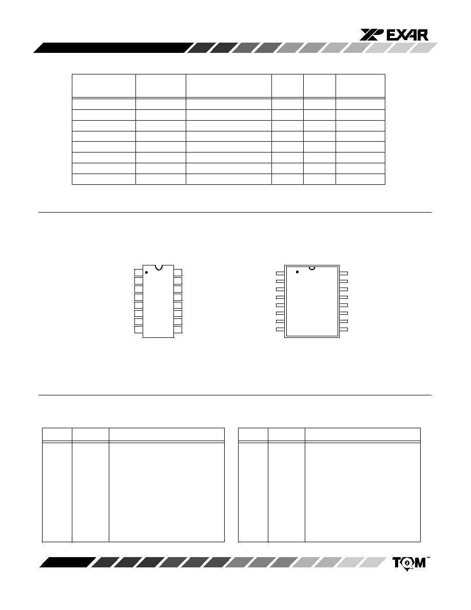
PIN CONFIGURATIONS
16 pin SOIC (Jedec, 0.300")
16 pin SOIC (Jedec, 0.150")
16 pin SOP (EIAJ, 5.5 mm)
N/C
N/C
BIT 8 (LSB)
BIT 7
BIT 6
R
FB
V
REF
V
DD
GND
(MSB) BIT 1
BIT 2
BIT 3
BIT 4
BIT 5
I
OUT1
I
OUT2
16
1
9
8
2
3
4
5
6
7
15
14
13
12
11
10
GND
(MSB) BIT 1
BIT 2
BIT 3
BIT 4
BIT 5
N/C
N/C
BIT 8 (LSB)
BIT 7
BIT 6
1
2
3
4
5
6
7
8
16
15
14
13
12
11
10
9
16 Pin PDIP (0.300")
R
FB
V
REF
V
DD
I
OUT1
I
OUT2
PIN OUT DEFINITIONS
1
I
OUT1
Current Output 1
2
I
OUT2
Current Output 2
3
GND
Ground
4
BIT 1
Bit 1 (MSB)
5
BIT 2
Bit 2
6
BIT 3
Bit 3
7
BIT 4
Bit 4
8
BIT 5
Bit 5
PIN NO.
NAME
DESCRIPTION
9
BIT 6
Bit 6
10
BIT 7
Bit 7
11
BIT 8
Bit 8
12
N/C
No Connection
13
N/C
No Connection
14
V
DD
Positive Power Supply
15
V
REF
Reference Input Voltage
16
R
FB
Internal Feedback Resistor
PIN NO.
NAME
DESCRIPTION
MP7523/XRD7523
3
Rev. 3.00
ELECTRICAL CHARACTERISTICS
(V
DD
= + 15 V, V
REF
= +10 V unless otherwise noted)
25
∞
C
Tmin to Tmax
Parameter
Symbol
Min
Typ
Max
Min
Max
Units
Test Conditions/Comments
STATIC PERFORMANCE
1
Resolution (All Grades)
N
8
8
Bits
Integral Non-Linearity
INL
LSB
Best Fit Straight Line
(Relative Accuracy)
(Max INL ≠ Min INL) / 2
J
+1/2
+1/2
K
+1/4
+1/4
Monotonicity
Guaranteed over temp
Differential Non-Linearity
DNL
LSB
All grades monotonic over full
J
+1
+1
temperature range.
K
+1
+1
Gain Error
GE
+1.5
+1.8
%
Using Internal R
FB
J
Digital Inputs = V
INH
K
Power Supply Rejection Ratio
PSRR
+200
+300
ppm/%
|
Gain/
V
DD
|
V
DD
= + 5%
J
Digital Inputs = V
INH
K
Output Leakage Current (Pin 1)
I
OUT1
+50nA
+200nA
nA
Digital Inputs = V
INL
J
K
Output Leakage Current (Pin 2)
I
OUT2
+50nA
+200nA
nA
Digital Inputs = V
INH
J
K
REFERENCE INPUT
Input Resistance
R
IN
5
20
5
20
k
V
OUT1
= V
OUT2
= 0 V
DIGITAL INPUTS
Logical "1" Voltage
V
IH
14.5
14.5
V
Logical "0" Voltage
V
IL
0.5
0.5
V
Input Leakage Current
I
LKG
+1
+1
µ
A
ANALOG OUTPUTS
Output Capacitance
2
C
OUT1
100
100
pF
DAC Inputs all 1's
C
OUT1
30
30
pF
DAC Inputs all 0's
C
OUT2
30
30
pF
DAC Inputs all 1's
C
OUT2
100
100
pF
DAC Inputs all 0's

MP7523/XRD7523
4
Rev. 3.00
25
∞
C
NOTES:
Specifications are subject to change without notice
ELECTRICAL CHARACTERISTICS (CON'T)
Tmin to Tmax
Parameter
Symbol
Min
Typ
Max
Min
Max
Units
Test Conditions/Comments
POWER SUPPLY
Functional Voltage Range
2
V
DD
5
16
5
16
V
Supply Current
I
DD
1.6
1.6
mA
All digital inputs = 0 V or all = 15 V
1
Full Scale Range (FSR) is 10V.
2
Guaranteed but not production tested.
3
Digital input levels should not go below ground or exceed the positive supply voltage, otherwise damage may occur.
4
Specified values guarantee functionality. Refer to other parameters for accuracy.
ABSOLUTE MAXIMUM RATINGS (T
A
= +25
∞
C unless otherwise noted)
1, 2
V
DD
to GND
+17 V
. . . . . . . . . . . . . . . . . . . . . . . . . . . . . .
Digital Input Voltage to GND GND ≠0.5 to V
DD
+0.5 V
I
OUT1
, I
OUT2
to GND
≠0.5 to 6.5 V
. . . . . . . . . . . . . . . . .
V
REF
to GND
+25 V
. . . . . . . . . . . . . . . . . . . . . . . . . . . . .
V
RFB
to GND
+25 V
. . . . . . . . . . . . . . . . . . . . . . . . . . . . .
Storage Temperature
≠65
∞
C to +150
∞
C
. . . . . . . . . . . .
Lead Temperature (Soldering, 10 seconds)
+300
∞
C
.
Package Power Dissipation Rating to 75
∞
C
CDIP, PDIP, SOIC
800mW
. . . . . . . . . . . . . . . . . . . .
Derates above 75
∞
C
11mW/
∞
C
. . . . . . . . . . . . . . . . .
NOTES:
1
Stresses above those listed under "Absolute Maximum Ratings" may cause permanent damage to the device. This is a
stress rating only and functional operation at or above this specification is not implied. Exposure to maximum rating
conditions for extended periods may affect device reliability.
2
Any input pin which can see a value outside the absolute maximum ratings
should be protected by Schottky diode clamps
(HP5082-2835) from input pin to the supplies.
APPLICATION NOTES
Refer to Section 8 in the 1995 Data Acquisition Products databook for Applications Information
MP7523/XRD7523
5
Rev. 3.00
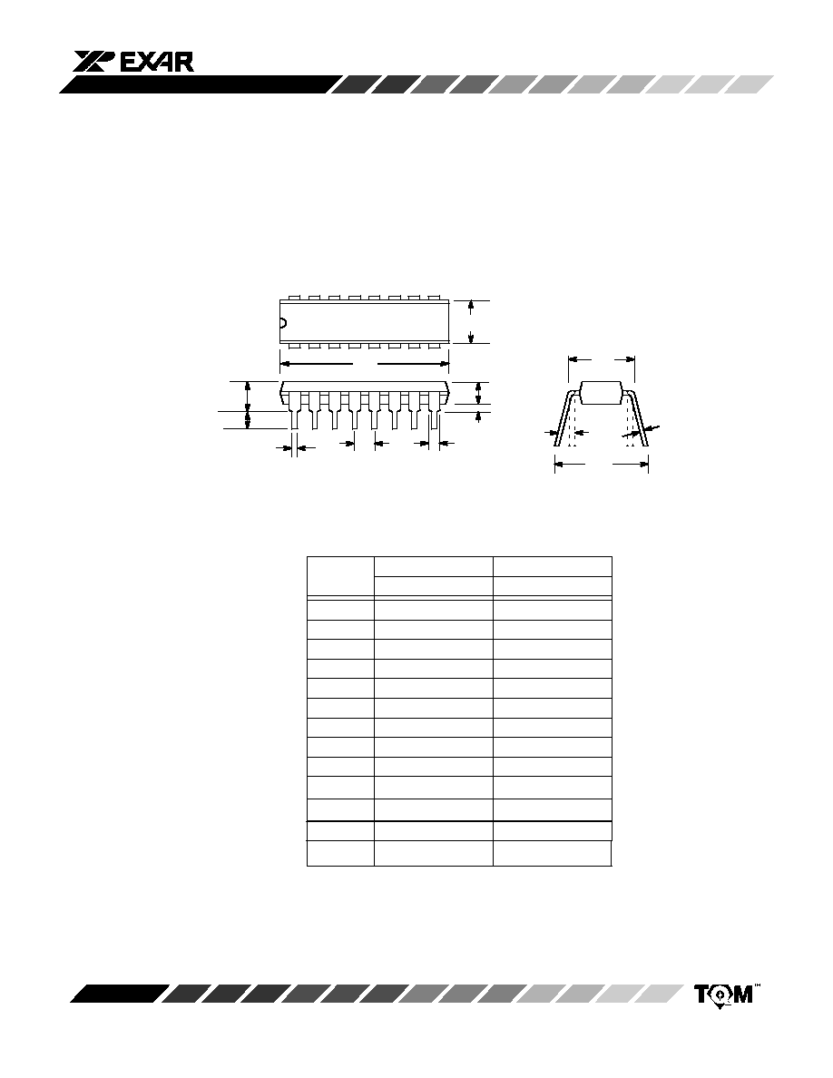
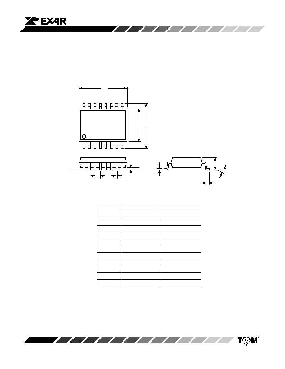
16 LEAD PLASTIC DUAL-IN-LINE
(300 MIL PDIP)
16
1
9
8
D
e
B
1
A
1
E
1
E
A
L
B
Seating
Plane
SYMBOL
MIN
MAX
MIN
MAX
INCHES
A
0.145
0.210
3.68
5.33
A
1
0.015
0.070
0.38
1.78
A
2
0.115
0.195
2.92
4.95
B
0.014
0.024
0.36
0.56
B
1
0.030
0.070
0.76
1.78
C
0.008
0.014
0.20
0.38
D
0.745
0.840
18.92
21.34
E
0.300
0.325
7.62
8.26
E
1
0.240
0.280
6.10
7.11
e
0.100 BSC
2.54 BSC
e
B
0.310
0.430
7.87
10.92
L
0.115
0.160
2.92
4.06
0
∞
15
∞
0
∞
15
∞
MILLIMETERS
e
B
A
2
C

MP7523/XRD7523
6
Rev. 3.00
SYMBOL
MIN
MAX
MIN
MAX
A
0.053
0.069
1.35
1.75
A
1
0.004
0.010
0.10
0.25
B
0.013
0.020
0.33
0.51
C
0.007
0.010
0.19
0.25
D
0.386
0.394
9.80
10.00
E
0.150
0.157
3.80
4.00
e
0.050 BSC
1.27 BSC
H
0.228
0.244
5.80
6.20
L
0.016
0.050
0.40
1.27
0
∞
8
∞
0
∞
8
∞
INCHES
MILLIMETERS
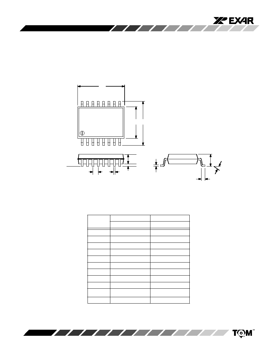
16 LEAD SMALL OUTLINE
(150 MIL JEDEC SOIC)
e
16
9
8
D
E
H
B
A
L
C
A
1
Seating
Plane
MP7523/XRD7523
7
Rev. 3.00
SYMBOL
MIN
MAX
MIN
MAX
A
0.093
0.104
2.35
2.65
A
1
0.004
0.012
0.10
0.30
B
0.013
0.020
0.33
0.51
C
0.009
0.013
0.23
0.32
D
0.398
0.413
10.10
10.50
E
0.291
0.299
7.40
7.60
e
0.050 BSC
1.27 BSC
H
0.394
0.419
10.00
10.65
L
0.016
0.050
0.40
1.27
0
∞
8
∞
0
∞
8
∞
INCHES
MILLIMETERS
16 LEAD SMALL OUTLINE
(300 MIL JEDEC SOIC)
e
16
9
8
D
E
H
B
A
L
C
A
1
Seating
Plane
MP7523/XRD7523
8
Rev. 3.00
16 LEAD EIAJ SMALL OUTLINE
(5.5 mm EIAJ SOP)
e
16
9
8
D
E
H
B
A
L
C
A
1
Seating
Plane
A
2
SYMBOL
MIN
MAX
MIN
MAX
A
1.80
2.40
0.071
0.095
A
1
0.02
0.20
0.001
0.008
A
2
1.80
2.20
0.079
0.087
B
0.30
0.50
0.012
0.020
C
0.13
0.20
0.005
0.008
D
9.9
10.5
0.390
0.414
E
5.30
5.70
0.209
0.224
e
1.27 BSC
0.050 BSC
H
7.80
8.20
0.307
0.323
L
0.30
0.90
0.012
0.035
0
∞
15
∞
0
∞
15
∞
INCHES
MILLIMETERS
1
Pin 1 Indexer

MP7523/XRD7523
9
Rev. 3.00
Notes

MP7523/XRD7523
10
Rev. 3.00
Notes
MP7523/XRD7523
11
Rev. 3.00
Notes

MP7523/XRD7523
12
Rev. 3.00
NOTICE
EXAR Corporation reserves the right to make changes to the products contained in this publication in order to im-
prove design, performance or reliability. EXAR Corporation assumes no responsibility for the use of any circuits de-
scribed herein, conveys no license under any patent or other right, and makes no representation that the circuits are
free of patent infringement. Charts and schedules contained here in are only for illustration purposes and may vary
depending upon a user's specific application. While the information in this publication has been carefully checked;
no responsibility, however, is assumed for inaccuracies.
EXAR Corporation does not recommend the use of any of its products in life support applications where the failure or
malfunction of the product can reasonably be expected to cause failure of the life support system or to significantly
affect its safety or effectiveness. Products are not authorized for use in such applications unless EXAR Corporation
receives, in writing, assurances to its satisfaction that: (a) the risk of injury or damage has been minimized; (b) the
user assumes all such risks; (c) potential liability of EXAR Corporation is adequately protected under the circum-
stances.
Copyright EXAR Corporation
Datasheet December 1996
Reproduction, in part or whole, without the prior written consent of EXAR Corporation is prohibited.