 | –≠–ª–µ–∫—Ç—Ä–æ–Ω–Ω—ã–π –∫–æ–º–ø–æ–Ω–µ–Ω—Ç: MP7542BD | –°–∫–∞—á–∞—Ç—å:  PDF PDF  ZIP ZIP |

MP7542
1
Rev. 2.00
FEATURES
∑
12-Bit DAC with a 4-Bit Parallel Address for 4 & 8-Bit
Microprocessor or Microcontroller Interface
∑
Nonlinearity +1/2 LSB Tmin to Tmax
∑
Latch-Up Free
∑
Low Sensitivity to Output Amplifier V
OS
∑
Low Output Capacitance
5 V CMOS
4-Bit Input, 12-Bit
Digital-to-Analog Converter
∑
+5 V Supply Operation
∑
Low Power Consumption: 40mW Max.
∑
Low Cost
∑
Serial Version: MP7543
GENERAL DESCRIPTION
The MP7542 is a precision, 12-bit CMOS 4-quadrant multi-
plying Digital-to-Analog Converter designed for direct interface
to 4 and 8-bit microprocessors.
The MP7542 consists of three 4-bit registers, a 12-bit DAC
register, address decoding logic, and a 12-bit CMOS multiplying
DAC. Data is loaded into the data registers in three 4-bit nibbles
and subsequently transferred to the 12-bit DAC register. All data
loading or data transfer operations are identical to the WRITE
cycle of a static RAM. A CLEAR input allows the 12-bit DAC reg-
ister to be reset to all zeros.
The MP7542 is manufactured using advanced thin-film on
monolithic double metal CMOS fabrication process. A unique
decoding technique is utilized yielding excellent accuracy and
stability.
The MP7542 reduces the additional linearity errors due to
output amplifier offset to only 330
µ
V per millivolt of offset versus
670
µ
V for the standard R-2R ladder CMOS DACs.
SIMPLIFIED BLOCK DIAGRAM
12-Bit Multiplying DAC
12-Bit DAC Register
H-Byte
Data
Register
M-Byte
Data
Register
L-Byte
Data
Register
Address
Decode
Logic
A0
A1
AGND
DB1
DB2
DB3 (MSB)
DGND
DB0 (LSB)
V
REF
R
FB
V
DD
I
OUT1
I
OUT2
CLR
WR
CS

MP7542
2
Rev. 2.00
ORDERING INFORMATION
Package
Type
Temperature
Range
Part No.
Ceramic Dip
MP7542AD
Ceramic Dip
MP7542BD
Ceramic Dip
MP7542SD*
Ceramic Dip
MP7542TD*
Plastic Dip
MP7542JN
Plastic Dip
MP7542KN
SOIC
MP7542JS
SOIC
MP7542KS
≠40 to +85
∞
C
≠40 to +85
∞
C
≠55 to +125
∞
C
≠55 to +125
∞
C
+1
+1
+1
+1
+1/2
+1/2
+1/2
+1/2
+2
+2
+2
+2
+1
+1
+1
+1
+14.5
+14.5
+14.5
+14.5
+14.5
+14.5
+14.5
+14.5
≠40 to +85
∞
C
≠40 to +85
∞
C
≠40 to +85
∞
C
≠40 to +85
∞
C
INL
(LSB)
DNL
(LSB)
Gain Error
(LSB)
*Contact factory for non-compliant military processing
PIN CONFIGURATIONS
AGND
DB3
DB2
DB1
DB0
DGND
A1
A0
16 Pin CDIP, PDIP (0.300")
D16, N16
1
2
3
4
5
6
7
8
16
15
14
13
12
11
10
9
R
FB
V
REF
V
DD
16
1
9
8
2
3
4
5
6
7
15
14
13
12
11
10
16 Pin SOIC (Jedec, 0.300")
S16
DGND
A1
A0
R
FB
V
REF
V
DD
I
OUT1
I
OUT2
AGND
DB3
DB2
DB1
DB0
I
OUT1
I
OUT2
See Packaging Section for Package Dimensions
CLR
WR
CS
CLR
WR
CS
PIN OUT DEFINITIONS
1
I
OUT1
DAC current output. Normally
terminated at op amp.
2
I
OUT2
DAC current output. Normally
terminated at ground.
3
AGND
Analog Ground
4
DB3
Data Input Bit 3 (MSB)
5
DB2
Data Input Bit 2
6
DB1
Data Input Bit 1
7
DB0
Data Input Bit 0 (LSB)
PIN NO.
NAME
DESCRIPTION
8
CS
Chip Select Input
9
WR
Write Input
10
A0
Address Bus Input
11
A1
Address Bus Input
12
DGND
Digital Ground
13
CLR
Clear Input
14
V
DD
+5 V Supply Input
15
V
REF
Reference Input
16
R
FB
DAC Feedback Resistor
PIN NO.
NAME
DESCRIPTION

MP7542
3
Rev. 2.00
ELECTRICAL CHARACTERISTICS
(V
DD
= + 5 V, V
REF
= +10 V unless otherwise noted)
25
∞
C
Tmin to Tmax
Parameter
Symbol
Min
Typ
Max
Min
Max
Units
Test Conditions/Comments
STATIC PERFORMANCE
1
Resolution (All Grades)
N
12
12
Bits
Integral Non-Linearity
INL
LSB
Best Fit Straight Line Spec.
(Relative Accuracy)
(Max INL ≠ Min INL) / 2
J, A, S
+1
+1
K, B, T
+1/2
+1/2
Differential Non-Linearity
DNL
LSB
Monotonicity
J, A, S
+2
+2
11 Bits Guaranteed
K, B, T
+1
+1
12 Bits Guaranteed
Gain Error
J, A, S, K, B, T
GE
+12.3
+14.5
LSB
Using Internal R
FB
Gain Temperature Coefficient
2
TC
GE
+2
ppm/
∞
C
Gain/
Temperature
Power Supply Rejection Ratio
PSRR
+50
+100
ppm/%
|
Gain/
V
DD
|
V
DD
= + 5%
Output Leakage Current
I
OUT
+10
+200
nA
DYNAMIC PERFORMANCE
R
L
=100
, C
L
=13pF
Current Settling Time
2
t
S
2.0
2.0
µ
s
Full Scale Change to 1/2 LSB
AC Feedthrough at I
OUT1
2
F
T
2.5
2.5
mV p-p
V
REF
= 10kHz, 20 Vp-p, sinewave
REFERENCE INPUT
Input Resistance
R
IN
5
10
20
5
20
k
DIGITAL INPUTS
3
Logical "1" Voltage
V
IH
3.0
3.0
V
Logical "0" Voltage
V
IL
0.8
0.8
V
Input Leakage Current
I
LKG
+1
+1
µ
A
Input Capacitance
2
C
IN
8
8
pF
ANALOG OUTPUTS
Output Capacitance
2
C
OUT1
260
260
pF
DAC Inputs all 1's
C
OUT1
100
100
pF
DAC Inputs all 0's
C
OUT2
50
50
pF
DAC Inputs all 1's
C
OUT2
210
210
pF
DAC Inputs all 0's
POWER SUPPLY
Supply Voltage
5
V
DD
+4.5
+5.5
+4.5
+5.5
V
Supply Current
I
DD
2.5
2.5
mA
All digital inputs = 0 V or all = 5 V

MP7542
4
Rev. 2.00
ELECTRICAL CHARACTERISTICS (CONT'D)
25
∞
C
Tmin to Tmax
NOTES:
Specifications are subject to change without notice
1
Full Scale Range (FSR) is 10V for unipolar mode.
2
Guaranteed but not production tested.
3
Digital input levels should not go below ground or exceed the positive supply voltage, otherwise damage may occur.
4
See timing diagram.
5
Specified values guarantee functionality. Refer to other parameters for accuracy.
Parameter
Symbol
Min
Typ
Max
Min
Max
Units
Test Conditions/Comments
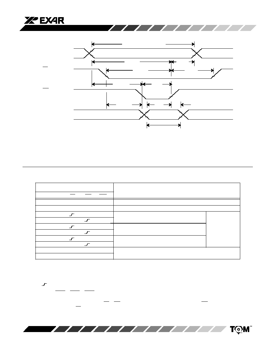
SWITCHING
CHARACTERISTICS
2, 4
WR Pulse Width
t
WR
120
220
ns
Address to WR Hold Time
t
AWH
50
65
ns
CS to WR Hold Time
t
CWH
50
100
ns
CLR Pulse Width
t
CLR
200
300
ns
Byte Loading, CS to WR Setup
t
CWS1
60
130
ns
Byte Loading, Address to WR Setup
t
AWS1
80
180
ns
Byte Loading, WR to Data Setup
t
DS
50
65
ns
Byte Loading, WR to Data Hold
t
DH
50
65
ns
DAC Loading, CS to WR Setup
t
CWS2
60
150
ns
DAC Loading, Address to WR Setup
t
AWS2
120
240
ns
ABSOLUTE MAXIMUM RATINGS (T
A
= +25
∞
C unless otherwise noted)
1, 2, 3
V
DD
to GND
+7 V
. . . . . . . . . . . . . . . . . . . . . . . . . . . . . . . . . . . .
Digital Input Voltage to GND (2)
GND ≠0.5 to V
DD
+0.5 V
.
I
OUT1
, I
OUT2
to GND
GND ≠0.5 to V
DD
+0.5 V
. . . . . . . . . . .
V
REF
to GND (2)
+25 V
. . . . . . . . . . . . . . . . . . . . . . . . . . . . . . .
V
RFB
to GND (2)
+25 V
. . . . . . . . . . . . . . . . . . . . . . . . . . . . . . .
AGND to DGND
+1 V
. . . . . . . . . . . . . . . . . . . . . . . . . . . . . . . . .
(Functionality Guaranteed +0.5 V)
Storage Temperature
≠65
∞
C to +150
∞
C
. . . . . . . . . . . . . . . . .
Lead Temperature (Soldering, 10 seconds)
+300
∞
C
. . . . . .
Package Power Dissipation Rating to 75
∞
C
CDIP, PDIP, SOIC
700mW
. . . . . . . . . . . . . . . . . . . . . . . . .
Derates above 75
∞
C
10mW/
∞
C
. . . . . . . . . . . . . . . . . . . . .
NOTES:
1
Stresses above those listed under "Absolute Maximum Ratings" may cause permanent damage to the device. This is a
stress rating only and functional operation at or above this specification is not implied. Exposure to maximum rating
conditions for extended periods may affect device reliability.
2
Any input pin which can see a value outside the absolute maximum ratings
should be protected by Schottky diode clamps
(HP5082-2835) from input pin to the supplies.
3
GND refers to AGND and DGND.
MP7542
5
Rev. 2.00
Figure 1. Timing Diagram
t
AWS1
ADDRESS BUS VALID
DATA
BUS VALID
t
CWS1
t
AWH
t
CWH
t
AWS2
t
WR
t
CWS2
t
DS
t
DH
V
INH
V
INL
V
INH
V
INL
V
INH
V
INL
A0 - A1
CS
WR
DB3 - DB0
MP7542 Operation
MP7542 Control Inputs
A
1
A
0
CS
WR
X
X
X
Resets DAC 12-bit register to code 0000 0000 0000
NOTES
1.
1 indicates logic HIGH
2.
0 indicates logic LOW
3.
X indicates don't care
4.
indicates LOW to HIGH transition
5.
MSB XXXX XXXX XXXX LSB
6.
Although positive-going edge of either CS or WR will load data register, timing is optimized by using WR to
latch data and using CS as a device enable.
Table 1. Truth Table
CLR
X
0
0
0
0
1
1
1
1
X
0
0
1
1
0
0
1
1
1
0
0
0
0
0
X
1
0
0
0
0
0
0
1
1
1
1
1
1
1
1
1
No operation; device not selected
Load LOW byte data register on edges as shown
Load MIDDLE byte data register on edges as shown
Load HIGH byte data register on edges as shown
Load 12-bit DAC register with data in LOW byte, MIDDLE
byte, & HIGH byte data registers
Load applicable
data register
with data at
D
0
- D
3
high
byte
middle
byte
low
byte