 | –≠–ª–µ–∫—Ç—Ä–æ–Ω–Ω—ã–π –∫–æ–º–ø–æ–Ω–µ–Ω—Ç: MP7543BD | –°–∫–∞—á–∞—Ç—å:  PDF PDF  ZIP ZIP |

MP7543
1
Rev. 2.00
5 V CMOS
Serial Input 12-Bit
Digital-to-Analog Converter
FEATURES
∑
12-Bit DAC with Serial Digital Input Interface
∑
Nonlinearity +1/2 LSB from Tmin to Tmax
∑
Lowest Sensitivity to Amplifier V
OS
∑
Low Output Capacitance
∑
Full 4-Quadrant Multiplication
∑
Latch-Up Free
∑
Asynchronous CLEAR Input
∑
Serial Load On Positive or Negative Strobes
∑
+5 V Supply Operation
∑
3 V Version: MP75L43
∑
4-Bit Parallel Version: MP7542
BENEFITS
∑
Compatible with Serial Addressing Systems
GENERAL DESCRIPTION
The MP7543 is a precision, 12-bit CMOS 4-quadrant multi-
plying Digital-to-Analog Converter designed for serial interface
applications.
The MP7543 consists of two 12-bit registers, control logic and
a 12-bit multiplying D/A converter. The input register (register A)
is a 12-bit serial-in parallel-out shift register. Serial data at the
SR1 pin is clocked into Register A on the leading or trailing edge
(user selected) of the strobe input, with the MSB loaded first.
Register B is a 12-bit parallel-in parallel-out register that follows
register A. The contents of register A are loaded into register B
under control of the Load inputs.
A CLEAR input is provided for the asynchronous resetting of
register B to all 0's.
The MP7543 is manufactured using an advanced thin film
monolithic CMOS fabrication process. A unique decoding tech-
nique is utilized yielding excellent accuracy and stability. 12-bit
linearity is achieved without laser trimming.
The MP7543 reduces the additional linearity errors due to
output amplifier offset to only 330
µ
V per millivolt of offset - half
the value of a standard R-2R CMOS DAC design approach.
SIMPLIFIED BLOCK DIAGRAM
12-Bit D/A Converter
DAC Register B
Register A
12-Bit Shift Register
Load
STB1
STB4
STB2
AGND
SRI
DGND
V
REF
R
FB
V
DD
I
OUT1
I
OUT2
CLR
LD1
LD2
STB3
MP7543
2
Rev. 2.00
ORDERING INFORMATION
Package
Type
Temperature
Range
Part No.
Ceramic Dip
MP7543AD
Ceramic Dip
MP7543BD
Ceramic Dip
MP7543TD*
Plastic Dip
MP7543JN
Plastic Dip
MP7543KN
PLCC
MP7543JP
PLCC
MP7543KP
≠40 to +85
∞
C
≠40 to +85
∞
C
≠55 to +125
∞
C
SOIC
MP7543JS
SOIC
MP7543KS
+1
+1
+1
+1
+1/2
+1/2
+1/2
+1/2
+1/2
+2
+2
+2
+2
+1
+1
+1
+1
+1
+14.5
+14.5
+14.5
+14.5
+14.5
+14.5
+14.5
+14.5
+14.5
≠40 to +85
∞
C
≠40 to +85
∞
C
≠40 to +85
∞
C
≠40 to +85
∞
C
≠40 to +85
∞
C
≠40 to +85
∞
C
Ceramic Dip
MP7543SD*
≠55 to +125
∞
C
+1
+2
+14.5
INL
(LSB)
Gain Error
(LSB)
DNL
(LSB)
*Contact factory for non-compliant military processing
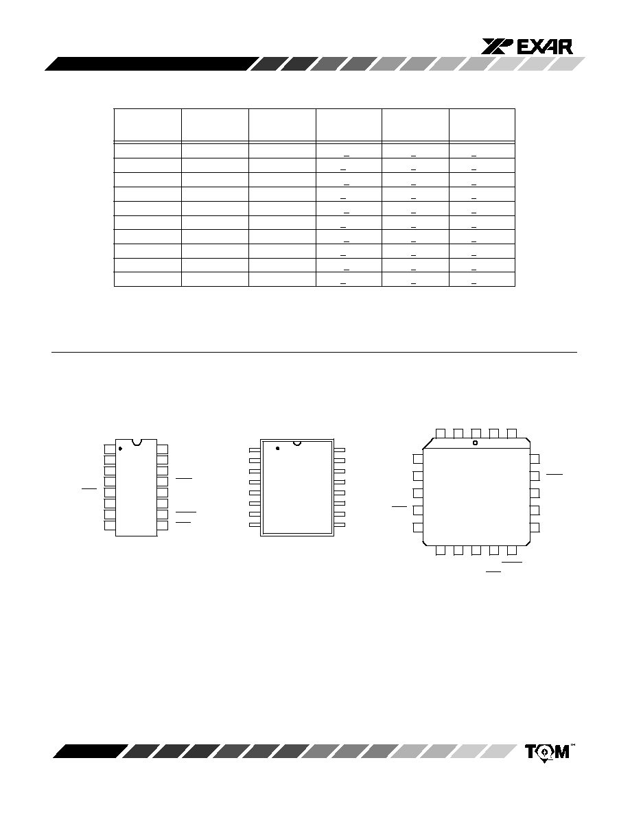
PIN CONFIGURATIONS
See Packaging Section for
Package Dimensions
AGND
STB1
N/C
SRI
STB2
DGND
STB4
1
2
3
4
5
6
7
8
16
15
14
13
12
11
10
9
16 Pin CDIP, PDIP (0.300")
D16, N16
3
2
1
20
19
9
10
11
12
13
4
5
6
7
8
18
17
16
15
14
20 Pin PLCC
P20
R
FB
V
REF
V
DD
16
1
9
8
2
3
4
5
6
7
15
14
13
12
11
10
See
Pin Out
at Left
16 Pin SOIC (Jedec, 0.300")
S16
AGND
STB1
SRI
STB2
STB4
DGND
V
DD
V
REF
R
FB
N/C
N/C
N/C
N/C
N/C
I
OUT1
I
OUT2
I
OUT1
I
OUT2
CLR
LD1
LD2
STB3
LD2
STB3
CLR
LD1

MP7543
3
Rev. 2.00
1
N/C
No Connection.
2
I
OUT1
DAC current output pin. Normally
terminated at op amp virtual ground.
3
I
OUT2
DAC current output pin. Normally
terminated at AGND.
4
AGND
Analog Ground.
5
STB1
Register A Strobe 1 input,
See Table 1.
6
N/C
No Connection.
7
LD1
DAC Register B Load 1 input. When
LD1 and LD2 go low the contents of
Register A are loaded into DAC
Register B.
8
N/C
No Connection.
9
SR1
Serial Data Input to Register A.
10
STB2
Register A Strobe 2 input,
See Table 1.
11
N/C
No Connection.
12
LD2
DAC Register B Load 2 input. When
LD1 and LD2 go low the contents of
Register A are loaded into DAC
Register B.
13
STB3
Register A Strobe 3 input,
See Table 1.
14
STB4
Register A Strobe 4 input,
See Table 1.
15
DGND
Digital Ground.
16
N/C
No Connection.
17
CLR
Register B CLEAR input (active
LOW), can be used to asynchronously
reset Register B to 0000 0000 0000.
18
V
DD
+5 V Supply Input.
19
V
REF
Reference input. Can be positive or
negative DC voltage or AC signal.
20
R
FB
DAC Feedback Resistor.
PIN OUT DEFINITIONS
1
I
OUT1
DAC current output pin. Normally
terminated at op amp virtual ground.
2
I
OUT2
DAC current output pin. Normally
terminated at AGND.
3
AGND
Analog Ground.
4
STB1
Register A Strobe 1 input,
See Table 1.
5
LD1
DAC Register B Load 1 input. When
LD1 and LD2 go low the contents of
Register A are loaded into DAC
Register B.
6
N/C
No Connection.
7
SRI
Serial Data Input to Register A.
8
STB2
Register A Strobe 2 input,
See Table 1.
9
LD2
DAC Register B Load 2 input. When
LD1 and LD2 go low the contents of
Register A are loaded into DAC
Register B.
10
STB3
Register A Strobe 3 input,
See Table 1.
11
STB4
Register A Strobe 4 input,
See Table 1.
12
DGND
Digital Ground.
13
CLR
Register B CLEAR input (active
LOW), can be used to asynchronously
reset Register B to 0000 0000 0000.
14
V
DD
+5 V Supply Input.
15
V
REF
Reference input. Can be positive or
negative DC voltage or AC signal.
16
R
FB
DAC Feedback Resistor.
PIN NO.
NAME
DESCRIPTION
PIN NO.
NAME
DESCRIPTION
PDIP, CDIP and SOIC
PLCC
MP7543
4
Rev. 2.00
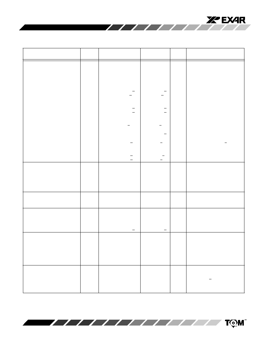
ELECTRICAL CHARACTERISTICS
(V
DD
= + 5 V, V
REF
= +10 V unless otherwise noted)
25
∞
C
Tmin to Tmax
Parameter
Symbol
Min
Typ
Max
Min
Max
Units
Test Conditions/Comments
STATIC PERFORMANCE
1
Resolution (All Grades)
N
12
12
Bits
Integral Non-Linearity
INL
LSB
Best Fit Straight Line Spec.
(Relative Accuracy)
(Max INL ≠ Min INL) / 2
J, A, S
+1
+1
K, B, T
+1/2
+1/2
Differential Non-Linearity
DNL
LSB
Monotonicity:
J, A, S
+2
+2
11 Bits Guaranteed
K, B, T
+1
+1
12 Bits Guaranteed
Gain Error
GE
LSB
Using Internal R
FB
J, A, K, B, S, T
+12.3
+14.5
Gain Temperature Coefficient
2
TC
GE
+2
ppm/
∞
C
Gain/
Temperature
Power Supply Rejection Ratio
PSRR
+50
+100
ppm/%
|
Gain/
V
DD
|
V
DD
= + 5%
Output Leakage Current
I
OUT
nA
J, K, A, B
+10
+10
S, T
+10
+200
DYNAMIC PERFORMANCE
Current Output Settling Time
2
t
S
2
2
µ
s
R
L
=100
, C
L
=13pF
Full Scale Output Settles to
1/2 LSB of Final Value
AC Feedthrough at I
OUT1
2
F
T
2.5
2.5
mV p-p
V
REF
= 10kHz, 20 Vp-p, sinewave
REFERENCE INPUT
Input Resistance
R
IN
5
10
20
5
20
k
DIGITAL INPUTS
3
Logical "1" Voltage
V
IH
3.0
3.0
V
Logical "0" Voltage
V
IL
0.8
0.8
V
Input Leakage Current
I
LKG
+1
+1
µ
A
ANALOG OUTPUTS
2
Output Capacitance
C
OUT1
260
260
pF
DAC Inputs all 1's
C
OUT1
100
100
pF
DAC Inputs all 0's
C
OUT2
50
50
pF
DAC Inputs all 1's
C
OUT2
210
210
pF
DAC Inputs all 0's
POWER SUPPLY
Supply Voltage
V
DD
4.75
5.25
4.75
5.25
V
V
DD
= +5 V +5% for specified
performance
Supply Current
I
DD
2.5
2.5
mA
All digital inputs = 0 V or all = 5 V
MP7543
5
Rev. 2.00
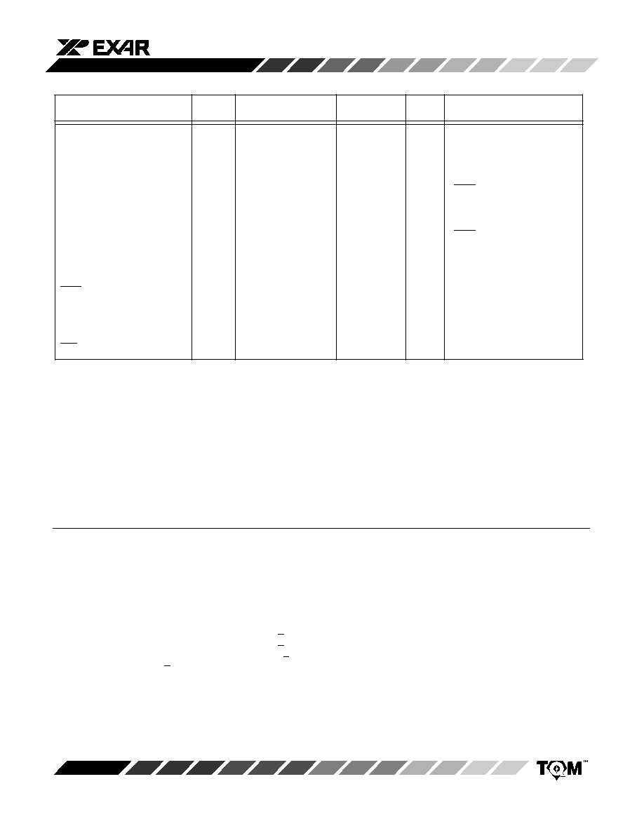
ELECTRICAL CHARACTERISTICS (CONT'D)
25
∞
C
Tmin to Tmax
NOTES:
Specifications are subject to change without notice
1
Full Scale Range (FSR) is 10V for unipolar mode.
2
Guaranteed but not production tested.
3
Digital input levels should not go below ground or exceed the positive supply voltage, otherwise damage may occur.
4
See timing diagram.
Parameter
Symbol
Min
Typ
Max
Min
Max
Units
Test Conditions/Comments
SWITCHING
CHARACTERISTICS
2, 4
Serial Input to Strobe Set-up Time
t
DS1
50
100
ns
STB1 used as a strobe
Serial Input to Strobe Set-up Time
t
DS4
0
0
ns
STB4 used as a strobe
Serial Input to Strobe Set-up Time
t
DS3
0
0
ns
STB3 used as a strobe
Serial Input to Strobe Set-up Time
t
DS2
20
40
ns
STB2 used as a strobe
Serial Input to Strobe Hold Time
t
DH1
30
60
ns
STB1 used as a strobe
Serial Input to Strobe Hold Time
t
DH4
80
160
ns
STB4 used as a strobe
Serial Input to Strobe Hold Time
t
DH3
80
160
ns
STB3 used as a strobe
Serial Input to Strobe Hold Time
t
DH2
60
120
ns
STB2 used as a strobe
SRI Data Pulse Width
t
SRI
80
160
ns
STB1 Pulse Width
t
STB1
80
160
ns
STB4 Pulse Width
t
STB4
100
200
ns
STB3 Pulse Width
t
STB3
100
200
ns
STB2 Pulse Width
t
STB2
80
160
ns
Load Pulse Width
t
LD1, 2
150
300
ns
Minimum time between strobing
t
ASB
0
0
ns
Reg. A and loading Reg. B
CLR pulse width
t
CLR
200
400
ns
ABSOLUTE MAXIMUM RATINGS (T
A
= +25
∞
C unless otherwise noted)
1, 2, 3
V
DD
to GND
+7 V
. . . . . . . . . . . . . . . . . . . . . . . . . . . . . . . . . . . .
Digital Input Voltage to GND (2)
GND ≠0.5 to V
DD
+0.5 V
.
I
OUT1
, I
OUT2
to GND
GND ≠0.5 to V
DD
+0.5 V
. . . . . . . . . . .
V
REF
to GND (2)
+25 V
. . . . . . . . . . . . . . . . . . . . . . . . . . . . . . .
V
RFB
to GND (2)
+25 V
. . . . . . . . . . . . . . . . . . . . . . . . . . . . . . .
AGND to DGND
+1 V
. . . . . . . . . . . . . . . . . . . . . . . . . . . . . . . . .
(Functionality Guaranteed +0.5 V)
Storage Temperature
≠65
∞
C to +150
∞
C
. . . . . . . . . . . . . . . . .
Lead Temperature (Soldering, 10 seconds)
+300
∞
C
. . . . . .
Package Power Dissipation Rating to 75
∞
C
CDIP, PDIP, SOIC, PLCC
700mW
. . . . . . . . . . . . . . . . . .
Derates above 75
∞
C
10mW/
∞
C
. . . . . . . . . . . . . . . . . . . . .
NOTES:
1
Stresses above those listed under "Absolute Maximum Ratings" may cause permanent damage to the device. This is a
stress rating only and functional operation at or above this specification is not implied. Exposure to maximum rating
conditions for extended periods may affect device reliability.
2
Any input pin which can see a value outside the absolute maximum ratings
should be protected by Schottky diode clamps
(HP5082-2835) from input pin to the supplies.
All inputs have protection diodes which will protect the device from short
transients outside the supplies of less than 100mA for less than 100
µ
s.
3
GND refers to AGND and DGND.