 | –≠–ª–µ–∫—Ç—Ä–æ–Ω–Ω—ã–π –∫–æ–º–ø–æ–Ω–µ–Ω—Ç: MP7610 | –°–∫–∞—á–∞—Ç—å:  PDF PDF  ZIP ZIP |
MP7610
Rev. 4.01
1
EXAR Corporation, 48720 Kato Road, Fremont, CA 94538 z (510) 668-7000 z (510) 668-7017
E
1998
FEATURES
∑ Eight Independent 14-Bit DACs with Output Amplifiers
∑ Low Power 320 mW (typ.)
∑ Serial Digital Data and Address Port (3-Wire Standard)
∑ 14-Bit Resolution, 12-Bit Accuracy
∑ Extremely Well Matched DACs
∑ Extremely Low Analog Ground Current (<60mA/Channel)
∑ +10 V Output Swing with +11.4 V Supplies
∑ Zero Volt Output Preset (Data = 10 .. 00)
∑ Rugged Construction -- Latch-Up Free
∑ Parallel Version: MP7611
Octal 14-Bit DAC Array
TM
D/A Converter with Output Amplifier
and Serial Data/Address mP Control Logic
APPLICATIONS
∑ Data Acquisition Systems
∑ ATE
∑ Process Control
∑ Self-Diagnostic Systems
∑ Logic Analyzers
∑ Digital Storage Scopes
∑ PC Based Controller/DAS
June 1998-3
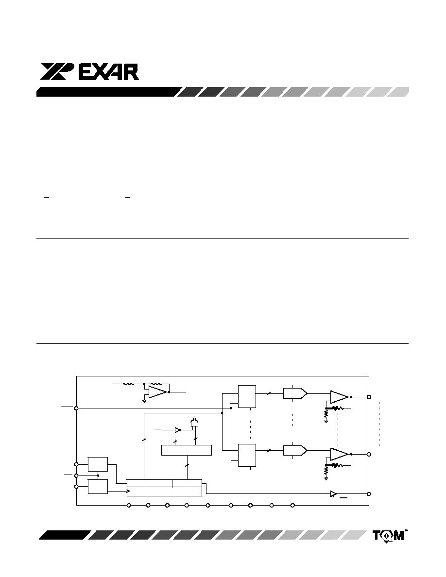
GENERAL DESCRIPTION
The MP7610 provides eight independent 14-bit resolution
Digital-to-Analog Converters with voltage output
amplifiers and a 3-wire standard serial digital address and
data port.
The output amplifier is capable of sinking and sourcing
5mA, and the output voltage settles to 12-bits in less than
30ms (typ.).
The MP7610 is equipped with a serial data (3-wire
standard) m-processor logic interface to reduce pin count,
package size, and board space.
Built using an advanced linear BiCMOS, these devices
offer rugged solutions that are latch-up free, and take
advantage of EXAR's patented thin-film resistor process
which exhibits excellent long term stability and reliability.
SIMPLIFIED BLOCK DIAGRAM
VO0
VO7
SDO
V
RP
V
RN
DAC0
DAC7
V
RP
V
RN
+
--
+
--
D
Q
XR XE
LAT0
LAT7
D
Q
XR XE
14
14
RST
V
RN
V
RP
+
--
Tri-State Buffer
XE0 - XE7
4 to 16 Decoder
Not Used
8
LD
14
4
SDI
CLK
LD
LAT
D
Q
EN
LAT
D
Q
EN
A0 to A3
D0 to D13
18-Bit Shift Register
V
EE
V
EE
V
CC
V
CC
AGND
AGND V
REF
DGND DV
DD
V
RP
XE0
XE7
LD
8

MP7610
2
Rev. 4.01
ORDERING INFORMATION
Package
Type
Temperature
Range
INL
(LSB)
Part No.
PLCC
--40 to +85
∞
C
MP7610AP
¶8
PLCC
--40 to +85
∞
C
MP7610BP
¶4
Res.
(Bits)
14
14
DNL
(LSB)
¶4
¶3
FSE
(LSB)
¶32
¶24
SOIC
--40 to +85
∞
C
MP7610AS
¶8
SOIC
--40 to +85
∞
C
MP7610BS
¶2
14
14
¶4
¶2
¶32
¶16
PLCC
0 to +70
∞
C
MP7610CP
¶2
14
¶2
¶16
SOIC
0 to +70
∞
C
MP7610CS
¶4
14
¶3
¶24
PIN CONFIGURATIONS
28 Pin SOIC (Jedec, 0.346")
VO0
VO1
VO2
VO3
V
EE
V
CC
V
REF
V
CC
V
EE
VO4
VO5
VO6
DGND
DV
DD
N/C or DV
DD
N/C
SDO
SDI
CLK
AGND
28
1
15
14
2
3
4
5
6
7
17
16
8
9
19
18
10
11
23
22
21
20
27
26
25
24
12
13
VO7
AGND
N/C
N/C
N/C
N/C
LD
RST
44 Pin PLCC
1
See the following page for
pin descriptions
MP7610
3
Rev. 4.01
PIN DESCRIPTION
SOIC
Pin #
PLCC
Pin #
Symbol
Description
1
2
AGND
Analog Ground
2
3
VO0
DAC 0 Output
3
4
VO1
DAC 1 Output
4
5
VO2
DAC 2 Output
5
6
VO3
DAC 3 Output
6
7
V
EE
Analog Negative Power Supply (--12 V)
7
9
V
CC
Analog Positive Power Supply (+12 V)
8
12
V
REF
Voltage Reference Input (+5 V)
9
13
V
CC
Analog Positive Power Supply (+12 V)
10
15
V
EE
Analog Negative Power Supply (--12 V)
11
18
VO4
DAC 4 Output
12
19
VO5
DAC 5 Output
13
20
VO6
DAC 6 Output
14
21
VO7
DAC 7 Output
15
24
AGND
Analog Ground
16
N/C
No Connection
17
26
RST
Reset all DACs to 0 V Output
18
N/C
No Connection
19
29
LD
Load Signal; Load Data to Selected DAC
20
31
CLK
Serial Data Clock
21
32
SDI
Serial Data Input
22
34
SDO
Shift Register Serial Output
23
N/C
No Connection
24
37
N/C
No Connection or DV
DD
25
40
DV
DD
Digital Positive Power Supply (+5 V)
26
N/C
No Connection
27
1, 8, 10, 11, 14,
16, 17, 22, 23,
25, 27, 28, 30,
33, 35, 36, 38,
39, 41, 42, 43
N/C
No Connection
28
44
DGND
Digital Ground

MP7610
4
Rev. 4.01
25
∞
C
Tmin to Tmax
ELECTRICAL CHARACTERISTICS
V
CC
= +12 V, V
EE
= --12 V, V
REF
= 5 V, DV
DD
= 5.0 V, T = 25∞C, Output Load = 5kW (unless otherwise noted)
Parameter
Symbol
Min
Typ
Max
Min
Max
Units
Test Conditions/Comments
STATIC PERFORMANCE
Resolution (All Grades)
N
14
Bits
Integral Non-Linearity
INL
LSB
End Point Linearity Spec
(Relative Accuracy)
A
¶8
¶8
B
¶4
¶4
C
¶2
¶2.5
Differential Non-Linearity
DNL
LSB
A
¶4
¶4
B
¶3
¶3
C
¶2
¶2.5
Positive Full Scale Error
+FSE
LSB
A
24
¶32
¶32
B
16
¶24
¶24
C
12
¶16
¶16
Positive Full Scale Error
D+FSE/
4
ppm/∞C
0∞C to 85∞C
Temperature Coefficient
DT
Negative Full Scale Error
--FSE
LSB
A
24
¶32
¶32
B
16
¶24
¶24
C
12
¶16
¶16
Negative Full Scale Error
D--FSE/
4
ppm/∞C
0∞C to 85∞C
Temperature Coefficient
DT
Bipolar Zero Offset
ZOFS
LSB
A
¶16
¶16
B
¶12
¶12
C
¶12
¶12
Bipolar Zero Offset
DZOFS/
2
ppm/∞C
0∞C to 85∞C
Temperature Coefficient
DT
INL Matching
DINL
LSB
A
¶8
¶8
B
¶6
¶6
C
¶6
¶6
All Channels Maximum Error
ME
LSB
with DAC 0 adjusted to minimum error
A
¶16
¶16
B
¶8
¶8
C
¶6
¶6
Bipolar Zero Matching
DZOFS
LSB
A
¶16
¶16
B
¶12
¶12
C
¶12
¶12
Full Scale Error Matching
DFSE
LSB
A
¶16
¶16
B
¶12
¶12
C
¶12
¶12
MP7610
5
Rev. 4.01
25
∞
C
Tmin to Tmax
ELECTRICAL CHARACTERISTICS (CONT'D)
Parameter
Symbol
Min
Typ
Max
Min
Max
Units
Test Conditions/Comments
DYNAMIC PERFORMANCE
Voltage Settling from LD
t
sd
30
50
50
ms
ZS to FS (20 V Step)
to VDAC Out
1
5k, 50pF load
Channel-to-Channel Crosstalk
6
CT
0.04
LSB
DC
Digital Feedthrough
1, 6
Q
--70
dB
CLK and Data to V
OUTi
Power Supply Rejection Ratio
PSRR
5
ppm/%
DV
EE
& DV
CC
= ±5%, ppm of FS
REFERENCE INPUTS
Impedance of V
REF
REF
350
700
1.05k
350
1.05k
W
See Application Hints for Driving
the reference input
V
REF
Voltage1,
2
V
REF
3.5
6
V
DIGITAL INPUTS
3
Logic High
V
IH
2.4
V
Logic Low
V
IL
0.8
V
Input Current
I
L
±10
mA
Input Capacitance
1
C
L
8
pF
ANALOG OUTPUTS
Output Swing
--V
EE
+1.4 V
CC
--1.4
V
Output Drive Current
--5
5
mA
Output Impedance
R
O
1
W
Output Short Circuit Current
I
SC
25
mA
+FS to AGND
30
mA
+FS to V
EE
40
mA
--FS to AGND
55
mA
--FS to V
CC
DIGITAL OUTPUTS
Output High Voltage
V
OH
4.5
V
Output Low Voltage
V
OL
0.5
V
POWER SUPPLIES
V
CC
Voltage
5
V
CC
V
REF
+1.5 12
12.75
V
REF
+1.5 12.75
V
V
EE
Voltage
5
V
EE
--12.75
--12
--5
--12.75
--5
V
DV
DD
Voltage
DV
DD
4.5
5
5.5
4.5
5.5
V
Positive Supply Current
I
CC
8
10
10
mA
Bipolar zero
Negative Supply Current
I
EE
15
20
20
mA
Bipolar zero
Digital Supply Current
I
DD
2
2
mA
Bipolar zero
Power Dissipation
PD
ISS
320
420
450
mW
Bipolar zero
ANALOG GROUND CURRENT
Per Channel
1
I
AGND
±60
mA
See Application Notes
DIGITAL TIMING
SPECIFICATIONS
1,4
V
IL
= 0, V
IH
= 5.0, C
L
= 20 pF
Input Clock Pulse Width
t
CH
, t
CL
60
ns
Data Setup Time
t
DS
15
ns
Data Hold Time
t
DH
15
ns
CLK to SDO Propagation Delay
t
PD
40
ns
DAC Register Load Pulse Width
t
LD
45
ns
Preset Pulse Width
t
PR
65
ns
Clock Edge to Load Time
t
CKLD1
140
ns
Note: t
LD
and t
CKLD2
cannot both
t
CKLD2
0
be min. since t
CKLD1
=t
CKLD2
+t
LD
LD Falling Edge to SDO
t
HZ1
50
ns
Tri-state Enable

MP7610
6
Rev. 4.01
25
∞
C
Tmin to Tmax
ELECTRICAL CHARACTERISTICS (CONT'D)
Specifications are subject to change without notice
Parameter
Symbol
Min
Typ
Max
Min
Max
Units
Test Conditions/Comments
DIGITAL TIMING
SPECIFICATIONS
1, 4
(CONT'D)
LD Rising Edge to SDO
t
HZ2
50
ns
Tri-state Disable
LD Rising Edge to CLK Enable
t
LDCK
50
ns
LD Set-up Time with Respect
t
LDSU
45
ns
to CLK
NOTES:
1
Guaranteed; not tested.
2
Specified values guarantee functionality.
3
Digital inputs should not go below digital GND or exceed DV
DD
supply voltage.
4
See Figures 2 and 3. All digital input signals are specified with t
R
= t
F
= 10 ns 10% to 90% and timed from a 50% voltage level.
5
For power supply values < ¶2£V
REF
, the output swing is limited as specified in Analog Outputs.
6
Digital feedthrough and channel-to-channel crosstalk are heavily dependent on the board layout and environment.
ABSOLUTE MAXIMUM RATINGS (TA = +25
∞
C unless otherwise noted)
1, 2
V
CC
to AGND
+16.5 V
. . . . . . . . . . . . . . . . . . . . . . . . . . .
V
EE
to AGND
--16.5 V
. . . . . . . . . . . . . . . . . . . . . . . . . . .
DV
DD
to DGND
+6.5 V
. . . . . . . . . . . . . . . . . . . . . . . . . .
V
REF
to DGND
+7.0 V
. . . . . . . . . . . . . . . . . . . . . . . . . . .
AGND to DGND
+1 V
. . . . . . . . . . . . . . . . . . . . . . . . . . . .
(Functionality guaranteed for ¶0.5 V only)
Digital Input & Output Voltage
to DGND
--0.5 to DV
DD
+0.5V
. . . . . . . . . . . . . . . . . . . .
Analog Inputs & Outputs
Indefinite Shorts to
. . . . . . .
V
CC
, V
EE
, DV
DD
, AGND, DGND (provided that power
dissipation of the package spec is not exceeded)
Operating Temperature Range
Extended Industrial
--40∞C to +85∞C
. . . . . . . . . . . . . .
Maximum Junction Temperature
--65∞C to 150∞C
. . .
Storage Temperature
150∞C
. . . . . . . . . . . . . . . . . . . . . .
Lead Temperature (Soldering, 10 sec)
+300∞C
. . . . .
Package Power Dissipation Rating @ 75∞C
SOIC, PLCC
1150mW
. . . . . . . . . . . . . . . . . . . . . . . . . . .
Derates above 75∞C
15mW/∞C
. . . . . . . . . . . . . . . . . . . .
NOTES:
1
Stresses above those listed under "Absolute Maximum Ratings" may cause permanent damage to the device. This is a
stress rating only and functional operation at or above this specification is not implied. Exposure to maximum rating
conditions for extended periods may affect device reliability.
2
Any input pin which can see a value outside the absolute maximum ratings should be protected by Schottky diode clamps
(HP5082-2835) from input pin to the supplies. All inputs have protection diodes which will protect the device from short
transients outside the supplies of less than 100mA for less than 100
m
s.
APPLICATION NOTES
NOTE: When using these DACs to drive remote devices, the accuracy of the output can be improved by utilizing a remote analog
ground connection. The difference between the DGND and AGND should be limited to ¶300 mV to assure normal operation. If there
is any chance that the AGND to DGND can be greater than ¶1 V, we recommend two back-to-back diodes be used between DGND
and AGND to clamp the voltage and prevent damage to the DAC. Using a buffer between the remote ground location and AGND may
help reduce noise induced from long lead or trace lengths.

MP7610
7
Rev. 4.01
A3
A2
A1
A0
D13
D12
D11
D10
D9
D8
D0
1
0
SDI
(Data In)
CLK
LD
SDO
V
OUT
Previous Data
DAC Register
Loaded
A3 (1)
1
0
1
0
1
0
Figure 1. Serial Data Timing and Loading
Figure 2. Serial Data Input Timing (RST = "1")
Figure 3. Reset Operation
1
0
SDI
SDO
CLK
LD
V
OUT
t
CH
t
CL
t
PD
t
DH
t
DS
t
LDSU
t
HZ1
t
HZ2
HIGH Z
t
LDCK2
t
CKLD1
t
LD
t
SD
+2 LSB Band
t
CKLD2
1
0
1
0
1
0
+FS
--FS
Note:
(1) CLK should be high during the falling edge of LD to insure proper function of the shift register.
RST
t
PR
1
0
V
OUT
V
OUT
= 0 V
Note: Reset settling time is <t
SD
Note:
(1) Because A3 is available immediately after 18th clock edge of DATA Shift-in, only 17 clock cycles are
needed to complete the readback.
MSB
MP7610
8
Rev. 4.01
The MP7610 is equipped with a serial data (3-wire standard)
m
-processor logic interface to reduce pin count, package size,
and board wire (space). If the LD signal is high, the CLK signal
loads the digital input bits (SDI) into the shift register (4 bits ad-
dress A3 to A0 plus 14 bits data D13 to D0 for the MP7610). The
LD signal going low loads the data into the selected DAC. The
LD signal going low also disables the serial data (SDI), output
(SDO tri-stated) and the CLK input. This design tremendously
reduces digital noise and glitch transients into the DACs due to
free running CLK and SDI. Note also that the preset signal
(RST) resets all analog outputs to 0 volt regardless of digital in-
puts.
A3 A2 A1 A0
X
X
X
X
1
1
DAC 0
0
0
0
1
DAC 1
0
0
1
0
DAC 2
0
0
1
1
DAC 3
0
1
0
0
DAC 4
0
1
0
1
DAC 5
0
1
1
0
DAC 6
0
1
1
1
DAC 7
1
0
0
0
X
X
X
X
X
X
X
X
1
1
1
1
1
1
1
1
X
X
X
X
X
X
0
1
1
1
0
1
1
1
1
1
1
Function
LD
CLK
RST
Shift Data In
and Out
0
Æ
1
Repeat
Load DACs
1
Æ
0
1
Æ
0
1
Æ
0
1
Æ
0
1
Æ
0
1
Æ
0
1
Æ
0
Reset all DACs
to 0 V
No Operation
No Operation
Table 1. Digital Function Truth Table
Serial In/Serial Out
1
Æ
0
X
X
X
X
X
SDI
Data Input
Valid
X
X
X
X
X
X
X
X
X
X
X
SDO
Data Output
Valid
Hi-Z
Hi-Z
Hi-Z
Hi-Z
Hi-Z
Hi-Z
Hi-Z
Hi-Z
Hi-Z
Hi-Z
0
0
0
0
No Operation
Stop Shifting
Data In and
Out
X
X
X
X
0
1
Hi-Z
X
X
X
No Operation
Note: For timing information See Electrical Characteristics.
Table 2. MP7610 Ideal DAC Output vs. Input Code
Hex Code
Output Voltage = 2
∑
Vr (--1 +
O O O O
10
∑
(--1 + 0) = --10
1 F F F
10
∑
(--1 +
) = --1.22 mV
Binary Code
2
∑
D
16384
)
(Vr = +5 V)
00000000000000
01111111111111
16382
16384
10000000000000
16384
16384
2 O O O
10
∑
(--1 +
) = 0
10000000000001
16386
16384
2 O O 1
10
∑
(--1 +
) = 1.22 mV
11111111111111
32766
16384
3 F F F
10
∑
(--1 +
) = 9.99878
Note: See Electrical Characteristics for real system accuracy

MP7610
9
Rev. 4.01
SERIAL INTERFACE DIAGRAMS
Figure 4. Simplified Diagram
VRI1
VOI1
1
8
VRI2
VOI2
1
8
1
8
VRIn
VOIn
IC(n)
IC(2)
IC(1)
SDI LD
SDO
SDI LD
SDO
SDI LD
SDO
m
PC
Data
LD
CLK
Figure 5. Simplified Diagram
VRIm
VOIm
VRI1
VOI1
VRI2
VOI2
1
8
1
8
1
8
IC(n)
IC(2)
IC(1)
#1
#2
#n
n
SDI LD
SDO
SDI LD
SDO
SDI LD
SDO
m
PC
Data
CS or LD
CLK
Data Out
VRI1 VOI1
VRI2 VOI2
VRIn VOIn
IC(n)
IC(2)
IC(1)
SDI LD SDO1
SDI LD SDO2
SDI LD SDOm
1
2
2
n
n
Address
WR
(SDI) Data In
CLK
SDO
m
PC
Figure 6. Simplified Diagram
A
d
d
r
e
s
s
D
e
c
o
d
e
r

MP7610
10
Rev. 4.01
A0 to A15
02
R/W
DBO to DB7
MC6800
8
16
E1
E3
E2
A0 to A2
3
16
8
74LS138
Address
Decoder
SDI
DB7
RST
LD
CLK
Data Bus
Address Bus
From SYSTEM RESET
NOTES
1.
Execute consecutive memory write instructions while manipulating the data between WRITEs so that each
WRITE presents the next bit.
2.
The serial data loading is triggered by the CLK pulse which is asserted by a decoded memory WRITE to
memory location 2000, R/W, and 02. A WRITE to address 4000 transfers data from input shift register to DAC
register.
Figure 7. MC6800 Interface
Figure 8. 8085 Interface
ALE
WR
SOD
8085
8212
8
8
8
Address Bus
Data Bus
+5
E1
E3
E2
A0 to A2
3
74LS138
Address
Decoder
SDI
LD
RST
CLK
From SYSTEM RESET
NOTES:
1.
Clock generated by WR and decoding address 8000.
2.
Data is clocked in the DAC shift register by executing memory write instructions. The clock input is generated
by decoding address 8000 and WR. Data is then loaded into the DAC register with a memory write instruction
to address 4000.
3.
Serial data must be present in the right justified format in registers H & L of the microprocessor.

MP7610
11
Rev. 4.01
PERFORMANCE CHARACTERISTICS
Graph 1. Typical Output Settling Characteristic
V
REF
= 5 V, R
L
= 5K, C
L
= 500pF
11 V
0 V
--11 V
2.5mV
0 V
--2.5mV
V
OUT
V
OUT
Settling
50ms/Division
Graph 1 shows the typical output settling characteristic of the MP7610 Family for a RESET !ZS!FS!ZS series
of code transitions. The top graph shows the output voltage transients, while the bottom graph shows the differ-
ence between the output and the ideal output.
Graph 2. Linearity with
V
REF
= 5 V, All DACs, All Codes
0
16384
4
--4
1
4
-
B
I
T
L
S
B
CODE

MP7610
12
Rev. 4.01
Graph 3. DAC 0 INL vs. V
REF
Graph 4. DAC 0 DNL vs. V
REF
Graph 5. DAC 0 Linearity with
V
REF
= 5 V, V
OUT
= ¶10
Graph 6. DAC 0 Linearity with
V
REF
= 4.5 V, V
OUT
= ¶9
Graph 7. DAC 0 Linearity with
V
REF
= 4 V, V
OUT
= ¶8
Graph 8. DAC 0 Linearity with
V
REF
= 3.5 V, V
OUT
= ¶7
0
16384
4
--4
1
4
-
B
I
T
L
S
B
CODE
0
16384
4
--4
1
4
-
B
I
T
L
S
B
CODE
0
16384
4
--4
1
4
-
B
I
T
L
S
B
CODE
0
16384
4
--4
1
4
-
B
I
T
L
S
B
CODE

MP7610
13
Rev. 4.01
MP7610
Family
V
OUT
5k
500pF
C
L
50
V
O
I
2mA
CL = 500pF, 5nF, 50nF, 500nF
Figure 9. Circuit for Determining Typical Analog Output Pulse Response
Graph 9. Typical Response of the MP7610 Family Analog Output to
a Current Pulse with CL=500pF, 5nF, 50nF, 500nF
(See Figure 9. above)
2.0mA
0.0
400mV
--400mV
200mV
--200mV
0s
1.0ms
2.0ms
3.0ms
4.0ms
5.0ms
6.0ms
C
L
= 500pF
C
L
= 5nF
C
L
= 50nF
C
L
= 500nF
I
V
O
V
OUT

MP7610
14
Rev. 4.01
44 LEAD PLASTIC LEADED CHIP CARRIER
(PLCC)
Rev. 1.00
1
D
D1
A
A
1
D
D
1
D
3
A
0.165
0.180
4.19
4.57
A
1
0.090
0.120
2.29
3.05
A
2
0.020
------.
0.51
------
B
0.013
0.021
0.33
0.53
B
1
0.026
0.032
0.66
0.81
C
0.008
0.013
0.19
0.32
D
0.685
0.695
17.40
17.65
D
1
0.650
0.656
16.51
16.66
D
2
0.590
0.630
14.99
16.00
D
3
0.500 typ.
12.70 typ.
e
0.050 BSC
1.27 BSC
H1
0.042
0.056
1.07
1.42
H2
0.042
0.048
1.07
1.22
R
0.025
0.045
0.64
1.14
SYMBOL
MIN
MAX
MIN
MAX
INCHES
MILLIMETERS
B
A
2
B
1
e
Seating Plane
D
2
2
44
Note: The control dimension is the inch column
D
3
45∞ x H2
45∞ x H1
C
R

MP7610
15
Rev. 4.01
SYMBOL
MIN
MAX
MIN
MAX
A
0.093
0.104
2.35
2.65
A
1
0.004
0.012
0.10
0.30
B
0.013
0.020
0.33
0.51
C
0.009
0.013
0.23
0.32
D
0.706
0.718
17.93
18.24
E
0.340
0.350
8.64
8.89
e
0.050 BSC
1.27 BSC
H
0.460
0.485
11.68
12.32
L
0.016
0.050
0.40
1.27
a
0
∞
8
∞
0
∞
8
∞
INCHES
MILLIMETERS
28 LEAD SMALL OUTLINE
(350 MIL JEDEC SOIC)
Rev. 1.00
e
D
E
H
B
A
L
C
A
1
Seating
Plane
a
28
15
14
Note: The control dimension is the millimeter column
1

MP7610
16
Rev. 4.01
NOTICE
EXAR Corporation reserves the right to make changes to the products contained in this publication in order to im-
prove design, performance or reliability. EXAR Corporation assumes no responsibility for the use of any circuits de-
scribed herein, conveys no license under any patent or other right, and makes no representation that the circuits are
free of patent infringement. Charts and schedules contained here in are only for illustration purposes and may vary
depending upon a user's specific application. While the information in this publication has been carefully checked;
no responsibility, however, is assumed for inaccuracies.
EXAR Corporation does not recommend the use of any of its products in life support applications where the failure or
malfunction of the product can reasonably be expected to cause failure of the life support system or to significantly
affect its safety or effectiveness. Products are not authorized for use in such applications unless EXAR Corporation
receives, in writing, assurances to its satisfaction that: (a) the risk of injury or damage has been minimized; (b) the
user assumes all such risks; (c) potential liability of EXAR Corporation is adequately protected under the circum-
stances.
Copyright 1998 EXAR Corporation
Datasheet June 1998
Reproduction, in part or whole, without the prior written consent of EXAR Corporation is prohibited.