 | –≠–ª–µ–∫—Ç—Ä–æ–Ω–Ω—ã–π –∫–æ–º–ø–æ–Ω–µ–Ω—Ç: MP7611BP | –°–∫–∞—á–∞—Ç—å:  PDF PDF  ZIP ZIP |
MP7611
Rev. 3.01
EXAR Corporation, 48720 Kato Road, Fremont, CA 94538 z (510) 668-7000 z (510) 668-7017
E
1998
FEATURES
∑ Eight Independent Channel 14-Bit DACs with
Output Amplifiers
∑ Low Power 320 mW (typ.)
∑ Parallel Digital Data and Address Port
∑ Double Buffered Data Interface
∑ Readback of DAC Latches
∑ Zero Volt Output Preset (Data = 10 .. 00)
∑ 14-Bit Resolution, 12-Bit Accuracy
∑ Extremely Well Matched DACs
∑ Extremely Low Analog Ground Current (<60mA/Channel)
∑ +10 V Output Swing with +11.4 V Supplies
Octal 14-Bit DAC Array
TM
D/A Converter with Output Amplifier
and Parallel Data/Address mP Control Logic
∑ Rugged Construction -- Latch-Up Free
∑ Serial Version: MP7610
APPLICATIONS
∑ Data Acquisition Systems
∑ ATE
∑ Process Control
∑ Self-Diagnostic Systems
∑ Logic Analyzers
∑ Digital Storage Scopes
∑ PC Based Controller/DAS
June 1998-3
GENERAL DESCRIPTION
The MP7611 provides eight independent 14-bit resolution
Digital-to-Analog Converters with voltage output
amplifiers and a parallel digital address and data port.
Built using an advanced linear BiCMOS, these devices
offer rugged solutions that are latch-up free, and take
advantage of EXAR's patented thin-film resistor process
which exhibits excellent long term stability and reliability.
A standard m-processor and TTL/CMOS compatible
14-bit input data port loads the data into the pre-selected
DACS.
This device can easily be interfaced to a data bus, and
digital readback of each channel is available.
Typical DAC matching for C grade versions is 1.5 LSB
across all codes. The output amplifier is capable of
sinking and sourcing 5mA, and the output voltage settles
to 12-bits in less than 30ms (typ.).
ORDERING INFORMATION
Package
Type
Temperature
Range
INL
(LSB)
Part No.
PQFP
--40 to +85
∞
C
MP7611AE
¶8
PQFP
--40 to +85
∞
C
MP7611BE
¶4
Res.
(Bits)
14
14
DNL
(LSB)
¶4
¶3
FSE
(LSB)
¶32
¶24
PLCC
--40 to +85
∞
C
MP7611AP
¶8
PLCC
--40 to +85
∞
C
MP7611BP
¶4
14
14
¶4
¶3
¶32
¶24
PQFP
0 to +70
∞
C
MP7611CE
¶2
14
¶2
¶16
PLCC
0 to +70
∞
C
MP7611CP
¶2
14
¶2
¶16

MP7611
2
Rev. 3.01
SIMPLIFIED BLOCK DIAGRAM
VO0
VO7
+
--
+
--
LAT0B
LAT7B
V
RP
V
RN
V
RP
V
RN
DAC0
DAC7
D
Q
XR XE
D
Q
XR XE
14
14
LAT0A
D
Q
XRXE
LAT7A
D
Q
XR XE
RB0
RB7
XE0
XE7
V
EE
V
EE
V
CC
V
CC
AGND AGND V
REF
DGND DV
DD
V
RP
+
--
V
RN
V
RP
14
Bus
I/O
D0 - D13
14
XE0 - XE7
RB0 - RB7
Control
Logic
A0 - A2
LD1
RD
CS
R1
R2
LD2
3
8
8
V
REFN
PIN CONFIGURATIONS
33
23
22
12
1
11
34
44
Index
44-Pin PQFP (14 mm x 14 mm)
See the following
page for pin numbers
and descriptions
1
44-Pin PLCC
See the following
page for pin numbers
and descriptions

MP7611
Rev. 3.01
3
PIN OUT DEFINITIONS
29
1
N/C
No Connection
30
2
VO3
DAC 3 Output
31
3
V
EE
Analog Negative Power Supply (--12 V)
32
4
V
CC
Analog Positive Power Supply (+12 V)
33
5
N/C
No Connection or DV
DD
34
6
V
REF
Analog Voltage Reference Input (+5 V)
35
7
V
REFN
Analog Negative Voltage Reference
Output (--2.5 V)
36
8
V
CC
Analog Positive Power Supply (+12 V)
37
9
V
EE
Analog Negative Power Supply (--12 V)
38
10
VO4
DAC 4 Output
39
11
N/C
No Connection
40
12
VO5
DAC 5 Output
41
13
VO6
DAC 6 Output
42
14
VO7
DAC 7 Output
43
15
AGND
Analog Ground ( 0 V)
44
16
CS
Chip Select Enable
1
17
RD
Read Back Enable
2
18
R2
Second--Latch-Bank Reset Enable
3
19
R1
First--Latch-Bank Reset Enable
4
20
LD2
Second--Latch-Bank Load Enable
5
21
LD1
First--Latch-Bank Load Enable
6
22
A2
Digital Address Bit 2
7
23
A1
Digital Address Bit 1
8
24
A0
Digital Address Bit 0
9
25
DB0
Digital Input Data Bit 0
10
26
DB1
Digital Input Data Bit 1
11
27
DB2
Digital Input Data Bit 2
12
28
DB3
Digital Input Data Bit 3
13
29
DB4
Digital Input Data Bit 4
14
30
DB5
Digital Input Data Bit 5
15
31
DB6
Digital Input Data Bit 6
16
32
DB7
Digital Input Data Bit 7
17
33
DB8
Digital Input Data Bit 8
18
34
DB9
Digital Input Data Bit 9
19
35
DB10
Digital Input Data Bit 10
20
36
DB11
Digital Input Data Bit 11
21
37
DB12
Digital Input Data Bit 12
22
38
DB13
Digital Input Data Bit 13 (MSB)
23
39
DV
DD
Digital Positive Power Supply (+5 V)
24
40
DGND
Digital Ground (0 V)
25
41
AGND
Analog Ground (0 V)
26
42
VO0
DAC 0 Output
27
43
VO1
DAC 1 Output
28
44
VO2
DAC 2 Output
PLCC
PIN NO.
DESCRIPTION
NAME
PQFP
PIN NO.

MP7611
4
Rev. 3.01
25
∞
C
Tmin to Tmax
ELECTRICAL CHARACTERISTICS
V
CC
= +12 V, V
EE
= --12 V, V
REF
= 5 V, DV
DD
= 5.0 V, T = 25∞C, Output Load = 5kW (unless otherwise noted)
Parameter
Symbol
Min
Typ
Max
Min
Max
Units
Test Conditions/Comments
STATIC PERFORMANCE
Resolution (All Grades)
N
14
Bits
Integral Non-Linearity
INL
LSB
End Point Linearity Spec
(Relative Accuracy)
A
¶8
¶8
B
¶4
¶4
C
¶2
¶2.5
Differential Non-Linearity
DNL
LSB
A
¶4
¶4
B
¶3
¶3
C
¶2
¶2.5
Positive Full Scale Error
+FSE
LSB
A
24
¶32
¶32
B
16
¶24
¶24
C
12
¶16
¶16
Positive Full Scale Error
D
+FSE/
4
ppm/∞C
0∞C to 85∞C
Temperature Coefficient
D
T
Negative Full Scale Error
--FSE
LSB
A
24
¶32
¶32
B
16
¶24
¶24
C
12
¶16
¶16
Negative Full Scale Error
D
--FSE/
4
ppm/∞C
0∞C to 85∞C
Temperature Coefficient
D
T
Bipolar Zero Offset
ZOFS
LSB
A
¶16
¶16
B
¶12
¶12
C
¶12
¶12
Bipolar Zero Offset
D
ZOFS/
2
ppm/∞C
0∞C to 85∞C
Temperature Coefficient
D
T
INL Matching
D
INL
LSB
A
¶8
¶8
B
¶6
¶6
C
¶6
¶6
All Channels Maximum Error
ME
LSB
with DAC 0 adjusted to
minimum error
A
¶16
¶16
B
¶8
¶8
C
¶6
¶6
Bipolar Zero Matching
D
ZOFS
LSB
A
¶16
¶16
B
¶12
¶12
C
¶12
¶12
Full Scale Error Matching
D
FSE
LSB
A
¶16
¶16
B
¶12
¶12
C
¶12
¶12
MP7611
Rev. 3.01
5
25
∞
C
Tmin to Tmax
ELECTRICAL CHARACTERISTICS (CONT'D)
Parameter
Symbol
Min
Typ
Max
Min
Max
Units
Test Conditions/Comments
DYNAMIC PERFORMANCE
Voltage Settling from LD
t
sd
30
50
50
ms
ZS to FS (20 V Step)
to VDAC Out
1
5k, 50pF load
Channel-to-Channel Crosstalk
6
CT
0.04
LSB
DC
Digital Feedthrough
1, 6
Q
--70
dB
CLK and Data to V
OUTi
Power Supply Rejection Ratio
PSRR
5
ppm/%
DV
EE
& DV
CC
= +5%, ppm of FS
REFERENCE INPUTS
Impedance of V
REF
REF
350
700
1.05k
350
1.05k
W
See Application Hints for driving
the reference input
V
REF
Voltage1,
2
V
REF
3.5
6
V
DIGITAL INPUTS
3
Logic High
V
IH
2.4
V
Logic Low
V
IL
0.8
V
Input Current
I
L
+10
mA
Input Capacitance
1
C
L
8
pF
ANALOG OUTPUTS
Output Swing
--V
EE
+1.4 V
CC
--1.4
V
Output Drive Current
--5
5
mA
V
REFN
Output Drive Current
--10
+10
mA
For test purposes only
Output Impedance
R
O
1
W
Output Short Circuit Current
I
SC
25
mA
+FS to AGND
30
mA
+FS to V
EE
40
mA
--FS to AGND
55
mA
--FS to V
CC
DIGITAL OUTPUTS
Output High Voltage
V
OH
4.5
V
Output Low Voltage
V
OL
0.5
V
POWER SUPPLIES
V
CC
Voltage
5
V
CC
V
REF
+1.5 12
12.75
V
REF
+1.5 12.75
V
V
EE
Voltage
5
V
EE
--12.75
--12
--5
--12.75
--5
V
DV
DD
Voltage
DV
DD
4.5
5
5.5
4.5
5.5
V
Positive Supply Current
I
CC
8
10
10
mA
Bipolar zero
Negative Supply Current
I
EE
15
20
20
mA
Bipolar zero
Digital Supply Current
I
DD
2
2
mA
Bipolar zero
Power Dissipation
PD
ISS
320
420
450
mW
Bipolar zero
ANALOG GROUND CURRENT
Per Channel
1
I
AGND
±60
mA
See Application Notes
DIGITAL TIMING
SPECIFICATIONS
1,4
V
IL
= 0 V, V
IH
= 5 V, C
L
= 20 pF
Data Setup Time
t
DS
20
ns
Data Hold Time
t
DH
20
ns
Address Set-up Time
t
AS
100
ns
Address Hold Time
t
AH
0
ns
Chip Select to LD1 Set-up Time
t
CS1
6
ns
Chip Select to LD1 Hold Time
t
CH1
0
ns
LD1 Pulse Width
t
LD1W
50
ns
LD1 Negative Edge to LD2
t
LD1LD2
60
ns
Positive Edge
LD2 Pulse Width
t
LD2W
60
ns
Chip Select to RD Set-Up Time
t
CS2
6
ns
Chip Select to RD Hold Time
t
CH2
0
ns
MP7611
6
Rev. 3.01
25
∞
C
Tmin to Tmax
ELECTRICAL CHARACTERISTICS (CONT'D)
Specifications are subject to change without notice
NOTES:
Parameter
Symbol
Min
Typ
Max
Min
Max
Units
Test Conditions/Comments
DIGITAL TIMING
SPECIFICATIONS
1, 4
(CONT'D)
RD Pulse Width
t
RD
600
ns
High Z to Data Valid for Readback
t
DA
600
ns
Data Valid for Readback to High Z
t
DR
200
ns
R1 Pulse Width
t
R1W
100
ns
R2 Pulse Width
t
R2W
100
ns
1
Guaranteed; not tested.
2
Specified values guarantee functionality.
3
Digital inputs should not go below digital GND or exceed DV
DD
supply voltage.
4
See Figures 1, 2 and 3. All digital input signals are specified with t
R
= t
F
= 10 ns 10% to 90% and timed from a 50% voltage level.
5
For power supply values < ¶2£V
REF
, the output swing is limited as specified in Analog Outputs.
6
Digital feedthrough and channel-to-channel crosstalk are heavily dependent on the board layout and environment.
ABSOLUTE MAXIMUM RATINGS (TA = +25
∞
C unless otherwise noted)
1, 2
V
CC
to AGND
+16.5 V
. . . . . . . . . . . . . . . . . . . . . . . . . . .
V
EE
to AGND
--16.5 V
. . . . . . . . . . . . . . . . . . . . . . . . . . .
DV
DD
to DGND
+6.5 V
. . . . . . . . . . . . . . . . . . . . . . . . . .
VREF to DGND
+7.0 V
. . . . . . . . . . . . . . . . . . . . . . . . . .
Analog Outputs & Inputs
Infinite Shorts to V
CC
, V
EE
, DV
DD
, AGND and DGND
(provided that power dissipation of the package spec is
not exceeded)
AGND to DGND
+1 V
. . . . . . . . . . . . . . . . . . . . . . . . . . . .
(Functionality guaranteed for ¶0.5 V only)
Digital Input & Digital Output Voltage to:
DV
DD
+.5 V
. . . . . . . . . . . . . . . . . . . . . . . . . . . . . . . . . . .
DGND
--.5 V
. . . . . . . . . . . . . . . . . . . . . . . . . . . . . . . . .
Operating Temperature Range
Extended Industrial
--40∞C to +85∞C
. . . . . . . . . . . . . . .
Military
--55∞C to +125∞C
. . . . . . . . . . . . . . . . . . . . . . . . .
Maximum Junction Temperature
150∞C
. . . . . . . . . . . .
Storage Temperature Range
--65∞C to +150∞C
. . . . . .
Lead Temperature (Soldering, 10 sec)
+300∞C
. . . . .
Package Power Dissipation Rating to 75∞C
PQFP, PGA, PLCC
800mW
. . . . . . . . . . . . . . . . . .
Derates above 75∞C
11mW/∞C
. . . . . . . . . . . . . . . .
NOTES:
1
Stresses above those listed under "Absolute Maximum Ratings" may cause permanent damage to the device. This is a
stress rating only and functional operation at or above this specification is not implied. Exposure to maximum rating
conditions for extended periods may affect device reliability.
2
Any input pin which can see a value outside the absolute maximum ratings should be protected by Schottky diode clamps
(HP5082-2835) from input pin to the supplies. All inputs have protection diodes which will protect the device from short
transients outside the supplies of less than 100mA for less than 100
m
s.
APPLICATION NOTES
NOTE: When using these DACs to drive remote devices, the accuracy of the output can be improved by utilizing a remote analog
ground connection. The difference between the DGND and AGND should be limited to ¶300 mV to assure normal operation. If there
is any chance that the AGND to DGND can be greater than ¶1 V, we recommend two back-to-back diodes be used between DGND
and AGND to clamp the voltage and prevent damage to the DAC. Using a buffer between the remote ground location and AGND may
help reduce noise induced from long lead or trace lengths.

MP7611
Rev. 3.01
7
Data
Input/Output
Bus
Address
A0-A2
Chip Select
CS
Load Latch A
LD1
Load Latch B
LD2
1
0
1
0
1
0
1
0
1
0
+FS
--FS
Analog Output
t
DS
t
DH
t
AS
t
AH
t
CH1
t
CS1
t
LD1W
t
LD1LD2
t
LD2W
t
SD
don't care
don't care
Notes:
(1)
Chip Select (CS) and Load LATCHA (LD1) Signals follow the same timing constraints and are interchangeable
in the above diagram.
(2)
R1 = R2 = 1.
(3)
For the case where LD2 is in the low state, analog output would respond to the falling edge of LD1 (transparent mode).
Address
A0-A2
Chip Select
CS
Data Readback
RD
Digital Output Data
D0 to D113
don't care
t
AS
t
AH
t
CS2
t
RD
t
CH2
don't care
HIGH-Z
HIGH-Z
t
DR
t
DA
1
0
1
0
1
0
1
0
Notes:
(1)
Chip Select (CS) and Data Readback (RD) Signals follow the same timing constraints and are interchangeable
in the above diagram.
(2)
R1 = R2 = 1.
R1
R2
Reset first latch bank to
1000 . . . . .0000
t
R1W
t
R2W
Reset second latch bank to 1000 . . . . .0000 and analog
output to zero volt.
1
0
1
0
Figure 1. Loading Latch A and Updating Latch B
Figure 2. Read Back First Latch Bank of One DAC
Figure 3. Reset Operations

MP7611
8
Rev. 3.01
A standard
m
-processor and TTL/CMOS compatible input
data port loads the data into the pre-selected DACS. If CS = 0,
the chip accesses digital data on the bus. Then address bits A0
to A2 select the appropriate DAC and LD1 loads the data into the
first-latch-bank. When all 8-channels first-latch-banks are
loaded, then LD2 enables the second-latch-bank and updates
all 8-channels simultaneously. The selected DAC becomes
transparent (activity on the digital inputs appear at the analog
output) when both LD1 = LD2 = 0.
R1 = 0 resets the first-latch-bank. R2 = 0 resets the second-
latch-bank which sets the analog output to zero volts (data =
100...00), regardless of digital inputs.
0
Æ
1
Function
A2
A1 A0
Table 1. Octal Parallel Data Input 14-Bit DAC Truth Table
Load Latch 1 of DAC1
Load Latch 1 of DAC2
Load Latch 1 of DAC3
Load Latch 1 of DAC4
Load Latch 1 of DAC5
Load Latch 1 of DAC6
Load Latch 1 of DAC7
Load Latch 1 of DAC8
0
0
0
0
0
1
0
1
0
0
1
1
1
0
0
1
0
1
1
1
0
1
1
1
1
1
1
1
1
1
1
1
0
Æ
1
0
Æ
1
0
Æ
1
0
Æ
1
0
Æ
1
0
Æ
1
0
Æ
1
0
Æ
1
1
1
1
1
1
1
1
1
1
1
1
1
1
1
1
1
1
1
1
1
1
1
1
1
0
0
0
0
0
0
0
0
Load Latch 2 of DAC1
Æ
8
X
X
X
1
1
X
1
1
Read Latch 1 of DAC1
Read Latch 1 of DAC2
Read Latch 1 of DAC3
Read Latch 1 of DAC4
Read Latch 1 of DAC5
Read Latch 1 of DAC6
Read Latch 1 of DAC7
Read Latch 1 of DAC8
0
0
0
0
0
1
0
1
0
0
1
1
1
0
0
1
0
1
1
1
0
1
1
1
1
1
1
1
1
1
1
1
1
1
1
1
1
1
1
1
1
1
1
1
1
1
1
1
0
0
0
0
0
0
0
0
0
0
0
0
0
0
0
0
1
1
1
1
1
1
1
1
Reset Latch 1 of DAC1
Æ
8
Reset Latch 2 of DAC1
Æ
8
X
X
X
X
X
X
X
X
X
X
X
X
0
1
1
0
X
X
Note: 1: High, 0: Low, X: Don't Care
RD
LD1
LD2
CS
R1
R2
Note: For timing information see Electrical Characterist
ics

MP7611
Rev. 3.01
9
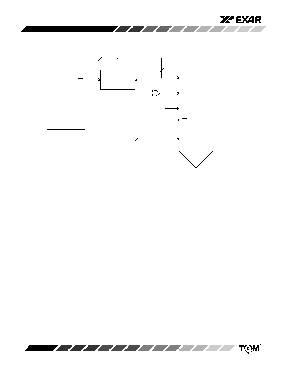
Figure 4. Simplified Parallel Logic Port
3-8
Decoder
3
8
8
8
To first latch bank enable
To switches across the first latch
bank for readback enable
To second latch bank enable
To reset all first latch bank
To reset all second latch bank
A0 to A2
LD1
CS
RD
LD2
R1
R2
8
Table 2. MP7611
Ideal DAC Output vs. Input Code
Hex Code
Output Voltage = 2
∑
Vr (--1 +
O O O O
10
∑
(--1 + 0) = --10
1 F F F
10
∑
(--1 +
) = --1.22 mV
Binary Code
2
∑
D
16384
)
(Vr = +5 V)
00000000000000
01111111111111
16382
16384
10000000000000
16384
16384
2 O O O
10
∑
(--1 +
) = 0
10000000000001
16386
16384
2 O O 1
10
∑
(--1 +
) = 1.22 mV
11111111111111
32766
16384
3 F F F
10
∑
(--1 +
) = 9.99878
Note: See Electrical Characteristics for real system accuracy
MP7611
10
Rev. 3.01
A0 to A15
AS
R
DB0 to DB16
m
P
16
Address
Decoder
3
A0 to A2
LD1
R1
R2
DB0 to DB11
or DB13
From System Reset
From System Reset
12 or 14
Figure 5. Parallel mP Interface
MP7611
Rev. 3.01
11
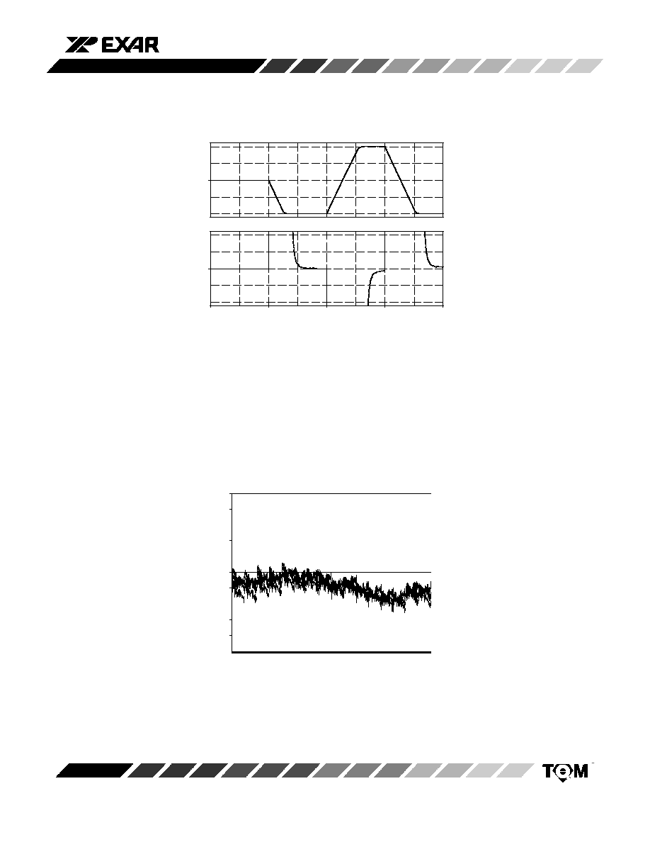
PERFORMANCE CHARACTERISTICS
Graph 1. Typical Output Settling Characteristic
V
REF
= 5 V, R
L
= 5K, C
L
= 500pF
11 V
0 V
--11 V
2.5mV
0 V
--2.5mV
V
OUT
V
OUT
Settling
50ms/Division
Graph 1 shows the typical output settling characteristic of the MP7610 Family for a RESET !ZS!FS!ZS series of code
transitions. The top graph shows the output voltage transients, while the bottom graph shows the difference between the output
and the ideal output.
Graph 2. Linearity with
V
REF
= 5 V, All DACs, All Codes
0
16384
4
--4
1
4
-
B
I
T
L
S
B
CODE

MP7611
12
Rev. 3.01
Graph 3. DAC 0 INL vs. V
REF
Graph 4. DAC 0 DNL vs. V
REF
Graph 5. DAC 0 Linearity with
V
REF
= 5 V, V
OUT
= ¶10
Graph 6. DAC 0 Linearity with
V
REF
= 4.5 V, V
OUT
= ¶9
Graph 7. DAC 0 Linearity with
V
REF
= 4 V, V
OUT
= ¶8
Graph 8. DAC 0 Linearity with
V
REF
= 3.5 V, V
OUT
= ¶7
0
16384
4
--4
1
4
-
B
I
T
L
S
B
CODE
0
16384
4
--4
1
4
-
B
I
T
L
S
B
CODE
0
16384
4
--4
1
4
-
B
I
T
L
S
B
CODE
0
16384
4
--4
1
4
-
B
I
T
L
S
B
CODE

MP7611
Rev. 3.01
13
MP7610
Family
V
OUT
5k
500pF
C
L
50
V
O
I
2mA
CL = 500pF, 5nF, 50nF, 500nF
Figure 6. Circuit for Determining Typical Analog Output Pulse Response
Graph 9. Typical Response of the MP7610 Family Analog Output to
a Current Pulse with CL=500pF, 5nF, 50nF, 500nF
(See Figure 9. above)
2.0mA
0.0
400mV
--400mV
200mV
--200mV
0s
1.0ms
2.0ms
3.0ms
4.0ms
5.0ms
6.0ms
C
L
= 500pF
C
L
= 5nF
C
L
= 50nF
C
L
= 500nF
I
V
O
V
OUT

MP7611
14
Rev. 3.01
A
0.110
0.134
2.80
3.40
A
1
0.010
0.014
0.25
0.35
A
2
0.100
0.120
2.55
3.05
B
0.014
0.020
0.35
0.50
C
0.005
0.009
0.13
0.23
D
0.667
0.687
16.95
17.45
D
1
0.547
0.555
13.90
14.10
e
0.039 BSC
1.00 BSC
L
0.026
0.37
0.65
0.95
a
0
∞
7
∞
0
∞
7
∞
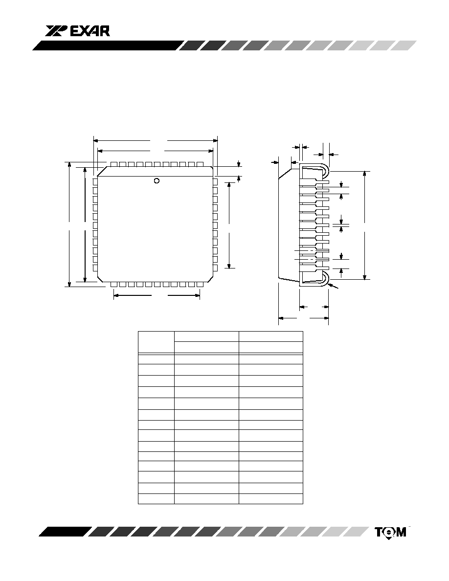
44 LEAD PLASTIC QUAD FLAT PACK
(14 mm x 14 mm QFP)
Rev. 1.00
SYMBOL
MIN
MAX
MIN
MAX
INCHES
MILLIMETERS
33
23
22
12
1
11
34
44
D
D
1
D
D
1
B
e
a
A
2
A
1
A
Seating Plane
Note: The control dimension is the millimeter column
L
C
MP7611
Rev. 3.01
15
44 LEAD PLASTIC LEADED CHIP CARRIER
(PLCC)
Rev. 1.00
1
D
D1
A
A
1
D
D
1
D
3
A
0.165
0.180
4.19
4.57
A
1
0.090
0.120
2.29
3.05
A
2
0.020
------.
0.51
------
B
0.013
0.021
0.33
0.53
B
1
0.026
0.032
0.66
0.81
C
0.008
0.013
0.19
0.32
D
0.685
0.695
17.40
17.65
D
1
0.650
0.656
16.51
16.66
D
2
0.590
0.630
14.99
16.00
D
3
0.500 typ.
12.70 typ.
e
0.050 BSC
1.27 BSC
H1
0.042
0.056
1.07
1.42
H2
0.042
0.048
1.07
1.22
R
0.025
0.045
0.64
1.14
SYMBOL
MIN
MAX
MIN
MAX
INCHES
MILLIMETERS
B
A
2
B
1
e
Seating Plane
D
2
2
44
Note: The control dimension is the inch column
D
3
45∞ x H2
45∞ x H1
C
R

MP7611
16
Rev. 3.01
NOTICE
EXAR Corporation reserves the right to make changes to the products contained in this publication in order to im-
prove design, performance or reliability. EXAR Corporation assumes no responsibility for the use of any circuits de-
scribed herein, conveys no license under any patent or other right, and makes no representation that the circuits are
free of patent infringement. Charts and schedules contained here in are only for illustration purposes and may vary
depending upon a user's specific application. While the information in this publication has been carefully checked;
no responsibility, however, is assumed for inaccuracies.
EXAR Corporation does not recommend the use of any of its products in life support applications where the failure or
malfunction of the product can reasonably be expected to cause failure of the life support system or to significantly
affect its safety or effectiveness. Products are not authorized for use in such applications unless EXAR Corporation
receives, in writing, assurances to its satisfaction that: (a) the risk of injury or damage has been minimized; (b) the
user assumes all such risks; (c) potential liability of EXAR Corporation is adequately protected under the circum-
stances.
Copyright 1998 EXAR Corporation
Datasheet June 1998
Reproduction, in part or whole, without the prior written consent of EXAR Corporation is prohibited.