 | –≠–ª–µ–∫—Ç—Ä–æ–Ω–Ω—ã–π –∫–æ–º–ø–æ–Ω–µ–Ω—Ç: MP7652AS | –°–∫–∞—á–∞—Ç—å:  PDF PDF  ZIP ZIP |

MP7652
1
Rev. 1.00
4-Channel Voltage Output
15 MHz, Input Bandwidth, 8-Bit Multiplying
DACs with 3-Wire Serial Digital Port
and Independent References
FEATURES
∑
Independent References
∑
4 Independent 2-Quadrant Multiplying 8-Bit DACs
∑
Dual Positive (+10 V and +5 V) Supplies or
Dual (+5 V) Supplies Capability
∑
High Speed:
≠
12.5 MHz Digital Clock Rate
≠
V
REF to
V
OUT
Settling Time: 150ns to 8≠bit
(typ)
≠
Voltage Reference Input Bandwidth:
15 MHz
∑
Low Power: 80mW
∑
Low AC Voltage Reference Feedthrough
∑
Excellent Channel-to-Channel Isolation
∑
DNL = +0.5 LSB, INL = +1 LSB (typ)
∑
DACs Matched to +0.5% (typ)
∑
Very Low Noise
∑
Low Harmonic Distortion: 0.25% typical with
V
REF
= 1 V p-p @ 1 MHz
∑
V
REF
/2 Output Preset Level
∑
Latch-Up Free
∑
ESD Protection: 2000 V Minimum
APPLICATIONS
∑
Direct High-Frequency Automatic Gain Control
∑
Video AGC & CCD Level AGC
∑
Convergence Adjustment for High-Resolution
Monitors (Workstations)
GENERAL DESCRIPTION
The MP7652 is ideal for digital gain control of high frequency
analog signals such as video, composite video, CCD and oth-
ers. The device includes 4-channels of high speed, wide
bandwidth, two quadrant multiplying, 8-bit accurate digital-to-
analog converter. It includes an output drive buffer per channel
capable of driving a +1mA (typ) load. DNL of better than +0.5
LSB is achieved with a channel-to-channel matching of typically
0.5%. Stability, matching, and precision of the DACs are
achieved by using MPS' thin film technology. Also, excellent
channel-to-channel isolation is achieved with EXAR's BiCMOS
process which cannot be achieved using a typical CMOS tech-
nology.
An open loop architecture (patent pending) provides wide
small signal bandwidth from V
REF
to output up to 15 MHz (typ),
fast output settling time of 150 ns, and excellent V
REF
feedthrough isolation. The bottom of each DAC reference string
is brought out separately for totally isolated operation. In addi-
tion, low distortion in the order of 0.25% with a 1 V p-p, 1 MHz
signal is achieved.
The combination of a constant input Z and the ability to vary
V
REFN
within V
CC
≠1.8 and V
EE
+1.5 V allows flexibility for opti-
mum system design.
The MP7652 is fabricated on a junction isolated, high speed
BiCMOS (BiCMOS IV
TM
) process with thin film resistors. This
process enables precision high speed analog/digital (mixed-
mode) circuits to be fabricated on the same chip.
ORDERING INFORMATION
Package
Type
Temperature
Range
Part No.
Gain Error
(% FSR)
SOIC
≠40 to +85
∞
C
MP7652AS
+0.5
+1
+1.5
Plastic Dip
≠40 to +85
∞
C
MP7652AN
+0.5
+1
+1.5
INL
(LSB)
DNL
(LSB)
MP7652
2
Rev. 1.00
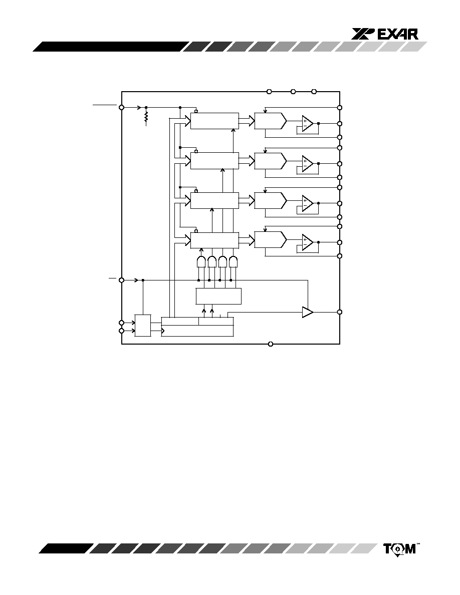
SIMPLIFIED BLOCK DIAGRAM
LATCH1
LATCH2
LATCH3
LATCH4
DAC1
2 to 4
Decoder
DB0 to DB7
A0 A1 X
X
12-BIT SHIFT REGISTER
DGND
V
DD
V
CC
V
EE
V
REFP1
PRESET
LD
V
OUT1
CLK
SDO
SDI
DAC1
DAC1
DAC1
V
REFN1
V
REFP2
V
OUT2
V
REFN2
V
REFP3
V
OUT3
V
REFN3
V
REFP4
V
OUT4
V
REFN4
V
DD
D
Q
EN
D
Q

MP7652
3
Rev. 1.00
PIN CONFIGURATIONS
24 Pin PDIP (0.300")
NN24
V
REFN1
DGND
24 Pin SOIC (Jedec, 0.300")
S24
N/C
V
DD
V
CC
V
EE
V
REFP1
V
REFP2
V
OUT2
PRESET
LD
V
REFP4
V
REFP3
V
OUT3
V
OUT1
CLK
SDO
SDI
V
OUT4
1
2
3
4
5
6
7
8
9
10
24
23
22
21
20
19
18
17
16
15
11
14
12
13
24
1
13
12
2
3
4
5
6
7
15
14
17
16
8
9
19
18
10
11
23
22
21
20
N/C
V
REFN2
N/C
V
REFN4
V
REFN3
PRESET
LD
V
REFP4
V
REFP3
V
OUT3
CLK
SDO
SDI
V
OUT4
N/C
V
REFN4
V
REFN3
V
REFN1
DGND
N/C
V
DD
V
CC
V
EE
V
REFP1
V
REFP2
V
OUT2
V
OUT1
N/C
V
REFN2
PIN OUT DEFINITIONS
1
N/C
No Connection
2
N/C
No Connection
3
V
DD
Digital Positive Supply
4
V
CC
Analog Positive Supply
5
V
EE
Analog Negative Supply
6
DGND
Digital Ground
7
V
REFN1
DAC 1 Negative Reference Input
8
V
OUT1
DAC 1 Output
9
V
REFP1
DAC 1 Positive Reference Input
10
V
REFP2
DAC 2 Positive Reference Input
11
V
OUT2
DAC 2 Output
12
V
REFN2
DAC 2 Negative Reference Input
13
V
REFN3
DAC 3 Negative Reference Input
PIN NO.
NAME
DESCRIPTION
14
V
OUT3
DAC 3 Output
15
V
REFP3
DAC 3 Positive Reference Input
16
V
REFP4
DAC 4 Positive Reference Input
17
V
OUT4
DAC 4 Output
18
V
REFN4
DAC 4 Negative Reference Input
19
SDI
Serial Data and Address Input
20
SDO
Serial Data Output
21
CLK
Shift Register Clock Input
22
LD
Load Data to Selected DAC
23
PRESET
Preset all DACs to 1/2
(V
REF
≠ V
REFN
). PRESET is
internally connected to V
DD
through 300 k
.
24
N/C
No Connection
PIN NO.
NAME
DESCRIPTION
MP7652
4
Rev. 1.00
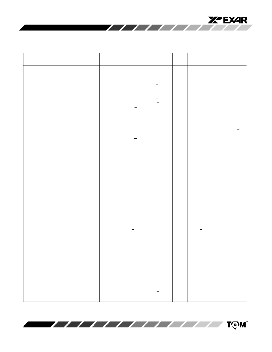
ELECTRICAL CHARACTERISTICS TABLE FOR DUAL SUPPLIES
Unless Otherwise Noted: V
DD
= 5 V, V
CC
= +5 V, V
EE
= ≠5 V, V
REFP
= 3 V and ≠3 V, T = 25
∞
C,
Output Load = Open, DGND=V
REFN
= 0 V
25
∞
C
Parameter
Symbol
Min
Typ
Max
Units
Test Conditions/Comments
DC CHARACTERISTICS
Resolution (All Grades)
N
8
Bits
Differential Non-Linearity
DNL
+0.8
LSB
Integral Non-Linearity
INL
+1
LSB
Monotonicity
Guaranteed
Gain Error
GE
+1.5
% FSR
FSR = Full Scale Range
1
Zero Scale Offset
Z
OFS
+50
mV
Output Drive Capability
I
O
+1
mA
REFERENCE/INV INPUTS
Impedance of V
REF
REF
6
18
k
Voltage Range
V
R
V
EE
+1.5
V
CC
≠1.8
V
V
REFP
Max Swing is V
REFN
+3 V
V
REFN
DC Voltage Range
INV Pos.
V
O
V
INV Neg.
V
EE
+ 1
V
DYNAMIC
CHARACTERISTICS
2
R
L
= 5 k
, C
L
= 20 pF
Input to Output Bandwidth
15
MHz
V
REFP
=1.6 Vp≠p, R
L
=5k
, to V
EE
Input to Output Settling Time
6
150
ns
V
REFP
=1.6Vp≠p, R
L
=5k
, to V
EE
Small Signal Voltage Reference
t
r
15
MHz
V
OUT
=50mV p-p above code 16
Input to Output Bandwidth
Small Signal Voltage Reference
t
r
15
MHz
V
OUT
=50mV p-p for all codes
Input to Output Bandwidth
Voltage Settling from V
REF
to
t
sr
275
ns
V
REFP
=0 to V
REFP
= 3V Step
6
V
DAC
Out
to 1 LSB
Voltage Settling from Digital
t
sd
275
ns
ZS to FS to 1 LSB
Code to V
DAC
Out
V
REF
Feedthrough
F
DT
TBD
dB
Codes=0 @ 1 MHz
Group Delay
GD
TBD
ns
Harmonic Distortion
T
HD
TBD
%
V
REFP
=1MHz Sine 3V p-p
Channel-to-Channel Crosstalk
C
T
TBD
dB
@ 1 MHz, single channel
Digital Feedthrough
Q
TBD
nVs
CLK to V
OUT
Power Supply
PSRR
+0.5
%/%
V=+5%
Rejection Ratio
POWER CONSUMPTION
Positive Supply Current
I
CC
12
mA
V
REFP
= 0 V
Negative Supply Current
I
EE
12
mA
V
REFP
= 0 V
Power Dissipation
P
DISS
80
mW
V
REFP
= 0 V, Codes = all 1
DIGITAL INPUT
CHACTERISTICS
Logic High
3
V
IH
2.4
V
Logic Low
3
V
IL
0.8
V
Input Current
I
L
+10
µ
A
Input Capacitance
2
C
L
8
pF
MP7652
5
Rev. 1.00
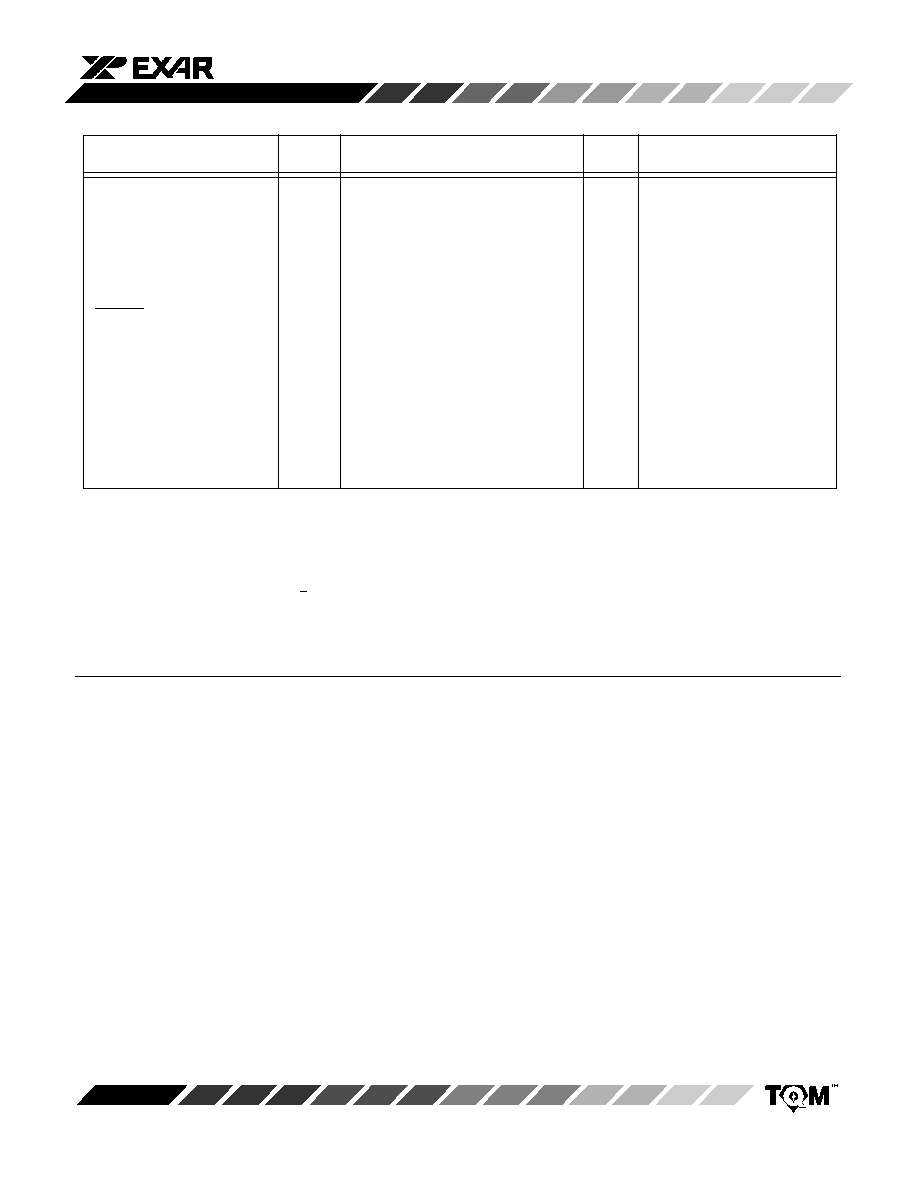
ELECTRICAL CHARACTERISTICS TABLE
Description
Symbol
Min
Typ
Max
Units
Conditions
DIGITAL TIMING
SPECIFICATIONS
2, 4
Input Clock Pulse Width
t
CH
, t
CL
60
ns
Data Setup Time
t
DS
70
ns
Data Hold Time
t
DH
0
ns
CLK to SDO Propagation Delay
t
PD
150
ns
DAC Register Load Pulse Width
t
LD
100
ns
PRESET Pulse Width
t
PR
50
ns
Clock Edge to Load Rising Edge
t
CKLD1
100
ns
Clock Edge to Load Falling Edge
t
CKLD2
0
ns
Load Falling Edge to SDO
t
HZ1
80
ns
Tri-state Enable
Load Rising Edge to SDO
t
HZ2
40
ns
Tri-state Disable
Load Falling Edge to CLK Disable
t
LDCK1
30
ns
Load Rising Edge to CLK Enable
t
LDCK2
60
ns
LD Set-up Time with Respect
t
LDSU
20
ns
to CLK
25
∞
C
NOTES
1
Full Scale Range (FSR) is 3V.
2
Guaranteed but not production tested.
3
Digital input levels should not go below ground or exceed the positive supply voltage, otherwise damage may occur.
4
See Figures 1 and 2.
5
For reference input pulse: t
R
= t
F
> 100 ns.
Specifications are subject to change without notice
ABSOLUTE MAXIMUM RATINGS (TA = +25
∞
C unless otherwise noted)
1, 2
V
CC
to V
REFN
+6.5 V
. . . . . . . . . . . . . . . . . . . . . . . . . . . . . . . . .
V
EE
to V
REFN
≠6.5 V
. . . . . . . . . . . . . . . . . . . . . . . . . . . . . . . . .
V
CC
to DGND
+13.0 V
. . . . . . . . . . . . . . . . . . . . . . . . . . . . . . . .
V
EE
to DGND
≠6.5 V
. . . . . . . . . . . . . . . . . . . . . . . . . . . . . . . . .
V
REFP
1-4 to DGND, V
REFN
V
CC
to V
EE
. . . . . . . . . . . . . . . . .
Digital Input & Output Voltage to DGND ≠0.5 to V
DD
+0.5 V
Operating Temperature Range
Extended Industrial
≠40
∞
C to +85
∞
C
. . . . . . . . . . . . . . . . . . .
Maximum Junction Temperature
≠65
∞
C to 150
∞
C
. . . . . . . . .
Storage Temperature
150
∞
C
. . . . . . . . . . . . . . . . . . . . . . . . . .
Lead Temperature (Soldering, 10 sec)
+300
∞
C
. . . . . . . . . . .
Package Power Dissipation Rating @ 75
∞
C
PDIP, SOIC
1000mW
. . . . . . . . . . . . . . . . . . . . . . . . . . . . .
Derates above 75
∞
C
6mW/
∞
C
. . . . . . . . . . . . . . . . . . . . . .
NOTES:
1
Stresses above those listed under "Absolute Maximum Ratings" may cause permanent damage to the device. This is a
stress rating only and functional operation at or above this specification is not implied. Exposure to maximum rating
conditions for extended periods may affect device reliability.
2
Any input pin which can see a value outside the absolute maximum ratings
should be protected by Schottky diode clamps
(HP5082-2835) from input pin to the supplies.
All inputs have protection diodes which will protect the device from short
transients outside the supplies of less than 100mA for less than 100
µ
s.