 | –≠–ª–µ–∫—Ç—Ä–æ–Ω–Ω—ã–π –∫–æ–º–ø–æ–Ω–µ–Ω—Ç: MP7680KE | –°–∫–∞—á–∞—Ç—å:  PDF PDF  ZIP ZIP |
MP7680
Rev. 3.10
EXAR Corporation, 48720 Kato Road, Fremont, CA 94538 z (510) 668-7000 z (510) 668-7017
E
1998
FEA TURES
∑ Exar Pioneered Segmented DAC Approach
∑ Four Double-Buffered 12-bit DACs on a Single Chip
∑ Independent Reference Inputs
∑ Lowest Gain Error in a Multiple DAC Chip
∑ Guaranteed Monotonic
∑ TTL/5 V CMOS Compatible Inputs
∑ Industry Standard Digital Interface
∑ Four Quadrant Multiplication
∑ Latch-Up Free
5 V CMOS 12-Bit
Quad Double-Buffered Multiplying
Digital-to-Analog Converter
BENEFITS
∑ Reduced Board Space; Lower System Cost.
∑ Independent Control of DACs
∑ Excellent DAC-to-DAC Matching and Tracking
APPLICA TIONS
∑ Function Generators
∑ Automatic Test Equipment
∑ Precision Process Controls
∑ Recording Studio Control Boards
June 2000-2
GENERAL
DESCRIPTIONS
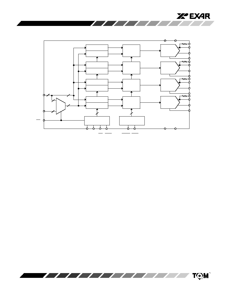
The MP7680 and the integrate four 12-bit four-quadrant-
multiplying DACs with independent reference inputs and
excellent matching characteristics. The MP7680 grades
offer 1/2, 1 and 2 LSB of relative accuracy. The superior
offers a low 2 LSB of gain error.
Each DAC has double-buffering (an 8 and 4-bit latch and
a 12-bit latch) between the data bus (DB11 - DB0) and the
DAC. The internal 4-bit mux allows the use of 8 or 16-bit
buses. The flexible latch control logic allows to update
one or more DACs simultaneously.
ORDERING
INFORMA TION
Package
Type
Temperature
Range
Part No.
PQFP
PQFP
Plastic Dip
Plastic Dip
-40 to +85∞∞C
MP7680JE
-40 to +85∞∞C
MP7680KE
-40 to +85∞∞C
-40 to +85∞∞C
MP7680JN
MP7680KN
+2
+4
+1
+2
+2
+4
+1
+2
+16
+16
+16
+16
INL
(LSB)
Gain Error
(LSB)
DNL
(LSB)
MP7680
2
Rev. 3.10
Figure 1. Simplified
Block Diagram
12-Bit
Latch
DAC D
8-Bit Latch
4-Bit Latch
DAC Latches
Control
Input Latches
Control
MUX
0
1
12-Bit
Latch
DAC C
8-Bit Latch
4-Bit Latch
12-Bit
Latch
DAC B
8-Bit Latch
4-Bit Latch
12-Bit
Latch
DAC A
8-Bit Latch
4-Bit Latch
1
8
A1 A0
DGND AGND
8
4
4
DB11 - DB4
(MSB)
DB3 - DB0
(LSB)
B1/B2
8
4
DV
DD
AV
DD
R
FBA
R
FBB
R
FBC
R
FBD
I
OUT1A
I
OUT2A
I
OUT1B
I
OUT2B
I
OUT1C
I
OUT2C
I
OUT1D
I
OUT2D
V
REFA
V
REFB
V
REFC
V
REFD
CS WR2
XFER WR2
MP7680
3
Rev. 3.10
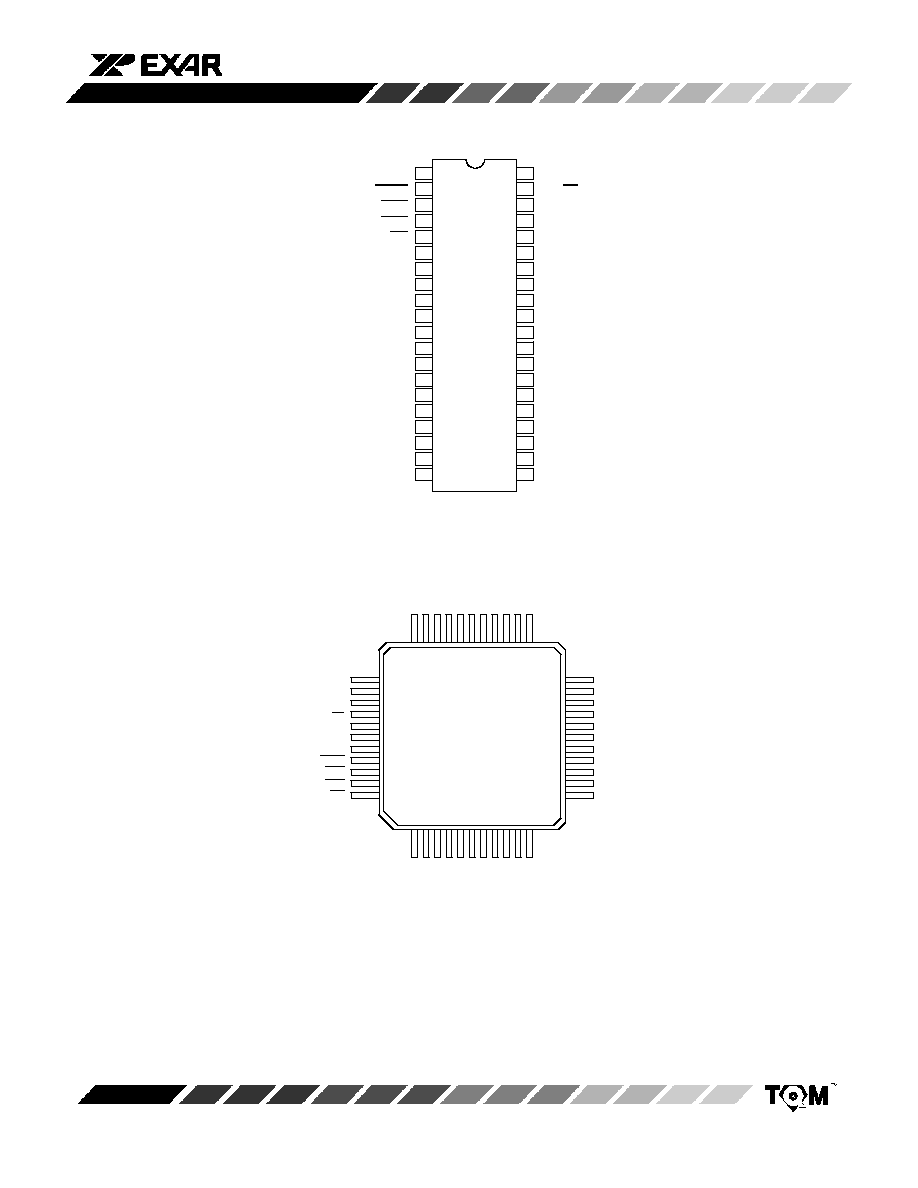
PIN CONFIGURA
TIONS
15
16
17
18
19
20
26
25
24
23
22
21
1
2
3
4
5
6
7
8
9
10
40
39
38
37
36
35
34
33
32
31
11
12
13
14
30
29
28
27
A1
XFER
WR2
WR1
CS
NC
V
REFA
R
FBA
I
OUT1A
I
OUT2A
I
OUT2B
I
OUT1B
R
FBB
V
REFB
(MSB) DB11
DB10
DB9
DB8
DB7
DB6
A0
B1/B2
DV
DD
AV
DD
DGND
AGND
V
REFD
R
FBD
I
OUT1D
I
OUT2D
I
OUT2C
I
OUT1C
R
FBC
V
REFC
DB0 (LSB)
DB1
DB2
DB3
DB4
DB5
40 Pin PDIP , (0.600")
33
23
22
12
1
11
34
44
44 Pin PQFP
See the following
page for
pin descriptions
DBO
V
I OUT1C
NC
IOUT2C
I OUT2D
I OUT1D
R
FBD
V
REFD
AGND
NC V
REF
A
R
FBA
IOUT1A IOUT2A NC IOUT2B IOUT1B RFBB VREFB DB1
1
DGND
AV DD
DVDD
B1/B2
AO
NC
A1
XFER
WR2
WR1
CS
DB1
DB2
DB3
DB4
DB5
NC
DB6
DB7
DB8
DB9
DB10
FBC
REFC
V
MP7680
4
Rev. 3.10
1
NC
No Connection
2
V
REFA
Reference Input for DAC A
3
R
FBA
Feedback Resistor for DAC A
4
I
OUT1A
Current Output A
5
I
OUT2A
Complement of Output A
6
NC
No Connection
7
I
OUT2B
Complement of Output B
8
I
OUT1B
Current Output B
9
R
FBB
Feedback Resistor for DAC B
10
V
REFB
Reference Input for DAC B
11-
DB11 to Input Data Bits 11 (MSB) to 6
16
DB6
17
NC
No Connection
18-
DB5-
Input Data Bits 5 to 0 (LSB)
23
DB0
24
V
REFC
Reference input for DAC C
25
R
FBC
Feedback Resistor for DAC C
26
I
OUT1C
Current Output C
27
I
OUT2C
Complement of Output C
28
NC
No Connection
29
I
OUT2D
Complement of Output D
30
I
OUT1D
Current Output D
31
R
FBD
Feedback Resistor for DAC D
32
V
REFD
Reference input for DAC D
33
AGND
Analog Ground
34
DGND
Digital Ground
35
AV
DD
Analog Power Supply
36
DV
DD
Digital Power Supply
37
B1/B2
Select Input Format (8/4 or 12 bits in)
38
A0
DAC Address Bit 0
39
NC
No Connection
40
A1
DAC Address Bit 1
41
XFER
Transfer: Updates all DAC's
42
WR2
Write 2: Gates the XFER Function
43
WR1
Write 1: Gates the DAC Selection
44
CS
Chip Select
PIN DESCRIPTION
1
A1
DAC Address Bit 1
2
XFER
Transfer: Updates all DAC's
3
WR2
Write 2: Gates the XFER Function
4
WR1
Write 1: Gates the DAC Selection
5
CS
Chip Select
6
NC
No Connection
7
V
REFA
Reference Input for DAC A
8
R
FBA
Feedback Resistor for DAC A
9
I
OUT1A
Current Output A
10
I
OUT2A
Complement of Output A
11
I
OUT2B
Complement of Output B
12
I
OUT1B
Current Output B
13
R
FBB
Feedback Resistor for DAC B
14
V
REFB
Reference Input for DAC B
15 -
DB11 to Input Data Bits 11 (MSB) to 0 (LSB)
26
DB0
27
V
REFC
Reference input for DAC C
28
R
FBC
Feedback Resistor for DAC C
29
I
OUT1C
Current Output C
30
I
OUT2C
Complement of Output C
31
I
OUT2D
Complement of Output D
32
I
OUT1D
Current Output D
33
R
FBD
Feedback Resistor for DAC D
34
V
REFD
Reference input for DAC D
35
AGND
Analog Ground
36
DGND
Digital Ground
37
AV
DD
Analog Power Supply
38
DV
DD
Digital Power Supply
39
B1/B2
Select Input Format (8/4 or 12 bits in)
40
A0
DAC Address Bit 0
40 Pin PDIP , CDIP
PIN NO.
NAME
DESCRIPTION
PIN NO.
NAME
DESCRIPTION
44 Pin PQFP
MP7680
5
Rev. 3.10
ELECTRICAL
CHARACTERISTICS
(V
D D
= + 5 V, V
R E F
= +10 V, I
O U T 1
= I
O U T 2
= DGND = AGND = 0 V Unless Otherwise
Noted)
25
∞
C
Tmin to Tmax
Parameter
Symbol
Min
Typ
Max
Min
Max
Units
Test Conditions/Comments
ST ATIC PERFORMANCE
1
Resolution (All Grades)
N
12
12
Bits
Integral Non-Linearity
INL
LSB
Best Fit Straight Line Spec.
(Relative Accuracy)
(Max INL - Min INL) / 2
K
+1
+1
J
+2
+2
Differential Non-Linearity
DNL
LSB
K
+1
+2.0
J
+4
+4.0
Gain Error
GE
LSB
Using Internal R
FB
K
+16
+16
J
+16
+16
Gain Temperature Coefficient
2
TC
GE
+2
ppm/∞∞C DGain/DTemperature
Power Supply Rejection Ratio
PSRR
+50
+70
ppm/%
|DGain/DV
DD
| DV
DD
= + 5%
Output Leakage Current
I
OUT
+50
+200
nA
I
OUT1
V
IN
= 0 V
I
OUT2
V
IN
= V
DD
DYNAMIC
PERFORMANCE
2
R
L
=100W, C
EXT
=13pF
Current Settling Time
t
S
1.0
ms
Full scale change to 1/2 LSB
REFERENCE
INPUT
Input Resistance
R
IN
3
5
7
3
7
kW
Voltage Input Range
2
V
IN
+10
+25
V
DIGIT AL INPUTS
Input High Voltage
V
IH
2.4
2.4
V
Input Low Voltage
V
IL
0.8
0.8
V
Input Current
I
LKG
+1
+4
mA
V
IN
= 0 V and V
DD
Input Capacitance
2
Data
C
IN
7.0
pF
Control
C
IN
7.0
pF
ANALOG
OUTPUTS
2
Output Capacitance
C
OUT1
100
pF
DAC all 1's
C
OUT1
50
pF
DAC all 0's
C
OUT2
50
pF
DAC all 1's
C
OUT2
100
pF
DAC all 0's
MP7680
6
Rev. 3.10
ELECTRICAL
CHARACTERISTICS
(CONT'D)
25
∞
C
Tmin to Tmax
Notes:
1
Full Scale Range (FSR) is 10V for unipolar mode.
2
Guaranteed
but not production
tested.
3
See timing diagram (Figure 2.).
4
DV
D D
and AV
D D
are connected
through the silicon substrate.
Connect
together at the package.
DC voltage differences
will cause undesirable
internal currents.
Specifications
are subject to change
without
notice
Parameter
Symbol
Min
Typ
Max
Min
Max
Units
Test Conditions/Comments
POWER
SUPPL Y 4
Functional Voltage Range
V
DD
4.5
5.5
4.5
5.5
V
Supply Current
I
DD
2
2
mA
Digital inputs = V
IL
or V
IH
1
1
mA
Digital inputs = 0 or 5 V
TIMING CHARACTERISTICS
2 , 3
Write Pulse Width
t
WR
75
85
ns
Chip Select Set-Up Time
t
CS
100
120
ns
Address Set-Up Time
t
AS
100
120
ns
Chip Select and Address Hold
t
H
0
0
ns
Time
Latch Select Set-Up Time
t
BS
120
150
ns
Latch Select Hold Time
t
BH
10
15
ns
Data Valid Set-Up Time
t
DS
100
120
ns
Data Valid Hold Time
t
DH
0
0
ns
Transfer Pulse Width
t
XFER
65
75
ns
Write Cycle (per DAC)
t
WC
175
200
ns
ABSOLUTE
MAXIMUM
RA TINGS
(TA = +25
∞
C unless otherwise
noted)
1, 2
V
DD
to AGND
-0.5 to +7 V
. . . . . . . . . . . . . . . . . . . . . . . . . . . .
V
DD
to DGND
-0.5 to +7 V
. . . . . . . . . . . . . . . . . . . . . . . . . . . .
Digital Input Voltage to DGND
GND -0.5 to V
DD
+0.5 V
. . . .
Any I
OUT1
, I
OUT2
to AGND
GND -0.5 to V
DD
+0.5 V
. . . . . . .
Any V
REF
to AGND
+25 V
. . . . . . . . . . . . . . . . . . . . . . . . . . . .
AGND to DGND
+1 V
. . . . . . . . . . . . . . . . . . . . . . . . . . . . . . . . .
(Functionality Guaranteed +0.5 V)
Any V
RFB
to AGND
+25 V
. . . . . . . . . . . . . . . . . . . . . . . . . . . .
Storage Temperature
-65
∞
C to +150
∞
C
. . . . . . . . . . . . . . . . . .
Lead Temperature (Soldering, 10 seconds)
+300
∞
C
. . . . . . .
Package Power Dissipation Rating to 75
∞
C
CDIP, PDIP, PQFP
800mW
. . . . . . . . . . . . . . . . . . . . . . . . .
Derates above 75
∞
C
11mW/
∞
C
. . . . . . . . . . . . . . . . . . . . .
Notes:
1
Stresses
above those listed under "Absolute
Maximum
Ratings" may cause permanent
damage to the device.
This is a
stress rating only and functional
operation
at or above this specification
is not implied.
Exposure
to maximum
rating
conditions
for extended
periods may affect device reliability .
2
Any input pin which can see a value outside the absolute
maximum
ratings should be protected
by Schottky
diode clamps
(HP5082-2835)
from input pin to the supplies.
All inputs have protection
diodes which will protect the device from short
transients
outside the supplies of less than 100mA for less than 100
m
s.

MP7680
7
Rev. 3.10
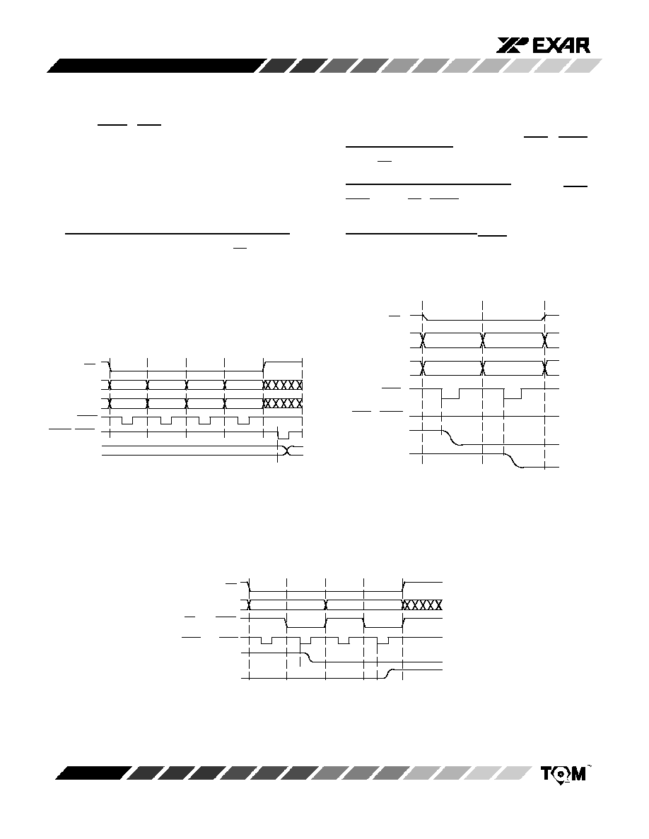
Figure 2. W rite Cycle T iming (Each DAC)
DATA
CS
WR1
XFER
WR2
VALID
VALID
B1/B2
NOTES:
1.
t
XFER
is the timing of the condition XFER = WR2
= Low .
2.
The timing of Figure 2. reproduces
graphically
the conditions
that all control signals must meet
in any of the many possible writing cycles (see
Theory of Operation).
t
CS
t
AS
t
BS
t
DS
t
WR
t
H
t
H
t
BH
t
DH
t
WC
t
XFER
A
0
, A
1
MP7680
8
Rev. 3.10
MUX
0
1
DAC
B1
Latch
B2
Latch
D
E
Q
D
E
Q
D
E
Q
12
4
8
8
4
12
4
8
8
4
DAC
B1
Latch
B2
Latch
D
E
Q
D
E
Q
D
E
Q
12
4
8
8
4
DAC
B1
Latch
B2
Latch
D
E
Q
D
E
Q
D
E
Q
12
4
8
8
4
DAC
B1
Latch
B2
Latch
D
E
Q
D
E
Q
D
E
Q
Latch
Address
Decoder
DA11 - DA0
LA11 - LA0
DAC LA TCHES
INPUT LA TCHES
DB11-DB4
(MSB)
DB3-DB0
(LSB)
B1/B2
A1 (MSB)
A0 (LSB)
CS
WR1
WR2
XFER
DB11-
DB8
Enable A
Enable B
Enable C
Enable D
DB11 - DB0
DC11 - DC0
DD11 - DD0
Transfer
Disable-B1
R
FBA
R
FBB
R
FBC
R
FBD
I
OUT1A
I
OUT2A
I
OUT1B
I
OUT2B
I
OUT1C
I
OUT2C
I
OUT1D
I
OUT2D
V
REFA
V
REFB
V
REFC
V
REFD
Figure 3. Latches
Control
Logic
THEOR Y OF OPERA TION
Digital Interface
Figure 3.
shows the internal control logic. The logic that
controls the writing of the input latches and the one that
controls the DAC latches are completely separated. It is
easy to understand how the MP7680/80A works by
understanding each basic operation.
W riting to Input Latches
By keeping B1/B2 = high, a 12-bit bus has direct access to
the 12 bits of the input latches. The condition CS = WR1 =
0 loads the values contained in the data bus DB11-DB0
into the input latch addresses by A
1
, A
0
(
Figure 4.
,
Table 1.
).
MP7680
9
Rev. 3.10
Table 1. DAC Selection
A 0
A 1
SELECTED
DAC
0
1
0
1
0
0
1
1
A
B
C
D
An 8-bit bus must use two cycles. The second cycle is
like the first one with the difference that B1/B2 = low
(
Figure 5.
) During the second cycle the condition B1/B2 =
low muxes DB11-DB8 to the B2 latches (
Figure 3.
).
Two important notes:
1) Timing diagrams show the inputs CS, A
1
, A
0
,
DB11-DB0 to be stable during the entire writing cycle.
In reality all the above signals can change (
Figure 4.
)
as long as they meet the timing conditions specified in
the Electrical Characteristic Table.
2) Only 16-bit bus cycles are shown in the next few exam-
ples of interface timing. It is possible to generate an
8-bit interface timing by replacing a single 12-bit write
cycle (
Figure 4.
) with a double 8-bit write cycles
(
Figure 5.
) 8-bit applications should ground inputs
DB3-DB0.
DATA
CS
WR1
B1/B2
Figure 4. 12 Bit W rite Cycle
or
Figure 5. 8-Bit Double W rite Cycle
WR1
CS
B1/B2
DATA
High
High
to B1
to B2
to B1 & B2
A
1
, A
0
A
1
, A
0
WR2
XFER
DA11-0
or
Figure 6. Transfer Cycles from Input Latches
to DAC Latches
or
I
OUT
t
S
MP7680
10
Rev. 3.10
Transferring
Data to the DAC Latches
Once one or all of the input latches have been loaded, the
condition XFER = WR2= low transfers the content of ALL
the input latches in the DAC latches. The output of the
DAC latches (DA11-DA0) changes and the DAC current
(I
OUT
) will reach a new stable value within the settling time
t
S
(
Figure 6.
).
Examples of DACs updating sequences:
1) Simultaneous updates of any number of DACs. The
system uses from one (two) to four (eight) cycles to
write from a 12 (8) bit bus into B1/B2 latches. One
transfer cycle updates the output of all DACs
(
Figure 7.
)
2) Individual DAC update. The condition WR2 = XFER =
low makes the DAC latches transparent. A writing to
the B1/B2 latches updates the DAC outputs (
Figure 8.
).
3) Automatic transfer to DAC latches. An 8-bit bus can
update any DAC with two cycles by connecting WR1 =
WR2 and B1/B2= XFER. This is the correct individual
DAC update for 8-bit busses (
Figure 9.
).
4) Transfer by a second device. A processor may load the
input latches while the final XFER pulse is left to an-
other device.
DATA
CS
WR1
Figure 7. Simultaneous
Updates
of DACs
XFER=WR2
= 0
= 1
= 2
= 3
Valid
Valid
Valid
Valid
A
0,
A
1
I
OUT1A, B, C, D
CS
DATA
WR1
WR2 = XFER
= 1
= 3
Figure 8. Individual
DAC Update
Valid
Valid
A
1
, A
0
I
OUT1B
I
OUT1D
CS
WR1 and WR2
Figure 9. Automatic
Transfer to DAC Latches
= 1
= 2
B1/B2 and XFER
A
1
, A
0
I
OUTB
I
OUTC

MP7680
11
Rev. 3.10
+
Figure 10. Digitally
Programmable
Quad Voltage Output + 10 V, + 5 V
0 V to -10 V
DAC A
+
0 V to +10 V
DAC B
+
+
0 V to +5 V
DAC C
0 V to -5 V
DAC D
8
9
10
13
12
11
28
29
30
33
32
31
+
REF01
6
2
4
5k
10k
10k
+10 V
7
10 V
14
+10 V
+15 V
+
6
4
2
10k
10k
5 V
27
34
REF02
5k
+5 V
+15 V
+5 V
R
FBA
I
OUT1A
I
OUT2A
R
FBB
I
OUT1B
I
OUT2B
R
FBC
I
OUT1C
I
OUT2C
R
FBD
I
OUT1D
I
OUT2D
V
OUTA
V
OUTB
V
OUTC
V
OUTD
V
REFA
V
REFB
V
REFC
V
REFD
+
Figure 11. "Clickless"
Audio Attenuator/Amplifier
DAC A
+
DAC B
+
+
DAC C
DAC D
Left
Channel
Input
+
+
Matched Pairs:
R
FBA
to RA
R
FBD
to RD
+
DAC A
DAC B
DAC C
DAC D
33k
10k
33k
10k
33k
10k
33k
10k
+
+5 V
10k
MP5010
10k
1.2 V
0.6 V
Figure 12. Quad DAC for Single +5 V Supply
R
FBA
R
FBB
R
FBC
R
FBD
Right
Channel
Input
RA
RD
Left
Channel
Output
(+10 V MAX)
Right
Channel
Output
(+10 V MAX)
+
+
+
V
OUTA
V
OUTB
V
OUTC
V
OUTD

MP7680
12
Rev. 3.10
Notes