 | –≠–ª–µ–∫—Ç—Ä–æ–Ω–Ω—ã–π –∫–æ–º–ø–æ–Ω–µ–Ω—Ç: MP8785A | –°–∫–∞—á–∞—Ç—å:  PDF PDF  ZIP ZIP |
MP8785
1
Rev. 2.00
CMOS
8-Bit High Speed
Analog-to-Digital Converter
FEATURES
∑
8-Bit Resolution
∑
20 MHz Sampling Rate
∑
DNL = +1/2 LSB, INL = +1 LSB (typ)
∑
Internal S/H Function
∑
Single Supply: 5 V
∑
V
IN
DC Range: 0 V to V
DD
∑
V
REF
DC Range: 1 V to V
DD
∑
Low Power: 85 mW typ. (excluding reference)
∑
Latch-Up Free
∑
ESD Protection: 1500 V Minimum
∑
20 Pin Package Available: MP8775
∑
Power Down Available: MP8776
∑
3 V Version: MP87L85
APPLICATIONS
∑
Digital Color Copiers
∑
Cellular Telephones
∑
CCD's and Scanners
∑
Video Capture Boards
GENERAL DESCRIPTION
The MP8785 is an 8-bit Analog-to-Digital Converter.
Designed using an advanced 5 V CMOS process, this part offers
excellent performance, low power consumption and latch-up
free operation.
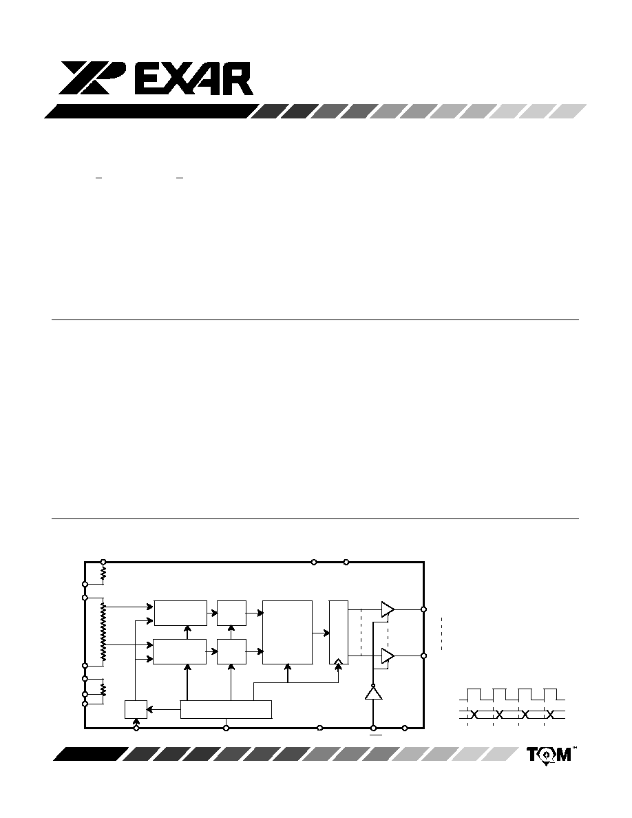
This device uses a two-step flash architecture to maintain low
power consumption at high conversion rates. The input circuitry
of the MP8785 includes an on-chip S/H function which allows
the user to digitize analog input signals between AGND and
AV
DD
. Careful design and chip layout have achieved a low ana-
log input capacitance. This reduces "kickback" and eases the
requirements of the buffer/amplifier used to drive the MP8785.
The designer can choose the internally generated reference
voltages by connecting V
RB
to V
RBS
and V
RT
to V
RTS
, or provide
external reference voltages to the V
RB
and V
RT
pins. The
internal reference generates 0.6 V at V
RB
and 2.6 V at V
RT
.
Providing external reference voltages allows easy interface to
any input signal range between AGND and AV
DD
. This also
allows the system to adjust these voltages to cancel zero scale
and full scale errors, or to change the input range as needed.
The device operates from a single +5 V supply. Power con-
sumption is 85 mW at F
S
= 20 MHz.
Specified for operation over the commercial / industrial (≠40
to +85
∞
C) temperature range, the MP8785 is available in Plas-
tic dual-in-line (PDIP) and Surface Mount (SOIC) packages in
EIAJ and Jedec.
SIMPLIFIED BLOCK AND TIMING DIAGRAM
MSB
Comparators
LSB
Comparators
Latch
Latch
Encoder
+
Error
Correction
F/F
S/H
Clock Logic
GND
DB7 (MSB)
DB0 (LSB)
OE
CLK
GND
V
RBS
V
RB
V
RT
V
RTS
AV
DD
DV
DD
/2
GND
GND
AV
DD
V
IN
N
N-3
N-2
N-1
N
CLK
DB7-
DB0
Sample
MP8785
2
Rev. 2.00
ORDERING INFORMATION
Package
Type
Temperature
Range
Part No.
DNL
(LSB)
SOIC (EIAJ)
≠40 to +85
∞
C
MP8785AR
INL
(LSB)
Plastic Dip (0.300")
≠40 to +85
∞
C
MP8785AN
3/4
1 1/2
3/4
1 1/2
SOIC (Jedec)
≠40 to +85
∞
C
MP8785AS
3/4
1 1/2
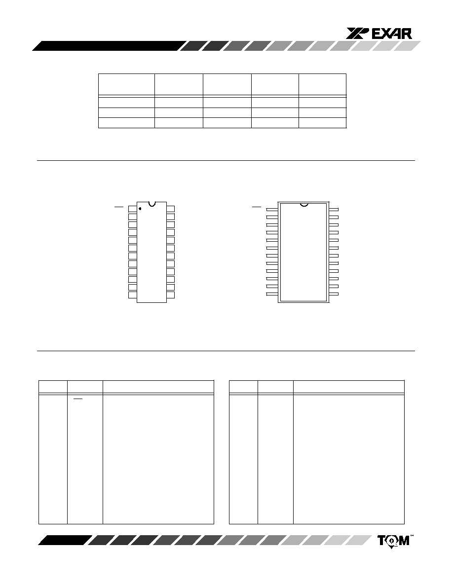
PIN CONFIGURATIONS
24 Pin PDIP (0.300")
NN24
1
2
3
4
5
6
7
8
9
10
24
23
22
21
20
19
18
17
16
15
11
14
12
13
DB0 (LSB)
DB1
DB2
DB3
DB4
DB5
DB6
DB7 (MSB)
CLK
DGND
DV
DD
DGND
V
RB
V
RBS
AGND
AGND
V
IN
AV
DD
V
RT
V
RTS
AV
DD
AV
DD
DV
DD
24
1
13
12
2
3
4
5
6
7
15
14
17
16
8
9
19
18
10
11
23
22
21
20
24 Pin SOIC (EIAJ, 0.300") ≠ RN24
24 Pin SOIC (Jedec, 0.300") ≠ S24
OE
DGND
V
RB
V
RBS
AGND
AGND
V
IN
AV
DD
V
RT
V
RTS
AV
DD
AV
DD
DV
DD
DB0 (LSB)
DB1
DB2
DB3
DB4
DB5
DB6
DB7 (MSB)
CLK
DGND
DV
DD
OE
See Packaging Section for Package Dimensions
PIN OUT DEFINITIONS
1
OE
Output Enable
2
DGND
Digital Ground
3
DB0
Data Output Bit 0 (LSB)
4
DB1
Data Output Bit 1
5
DB2
Data Output Bit 2
6
DB3
Data Output Bit 3
7
DB4
Data Output Bit 4
8
DB5
Data Output Bit 5
9
DB6
Data Output Bit 6
10
DB7
Data Output Bit 7 (MSB)
11
DV
DD
Digital Power Supply
12
CLK
Sampling Clock Input
PIN NO.
NAME
DESCRIPTION
13
DV
DD
Digital Power Supply
14
AV
DD
Analog Power Supply
15
AV
DD
Analog Power Supply
16
V
RTS
Generates 2.6 V if tied to V
RT
17
V
RT
Top Reference
18
AV
DD
Analog Power Supply
19
V
IN
Analog Input
20
AGND
Analog Ground
21
AGND
Analog Ground
22
V
RBS
Generates 0.6 V if tied to V
RB
23
V
RB
Bottom Reference
24
DGND
Digital Ground
PIN NO.
NAME
DESCRIPTION
MP8785
3
Rev. 2.00
ELECTRICAL CHARACTERISTICS TABLE
Unless Otherwise Specified: AV
DD
= DV
DD
= 5 V, FS = 15 MHz (50% Duty Cycle),
V
RT
= 2.6 V, V
RB
= 0.6 V, T
A
= 25
∞
C
25
∞
C
Parameter
Symbol
Min
Typ
Max
Units
Test Conditions/Comments
KEY FEATURES
Resolution
8
Bits
Sampling Rate
FS
20
MHz
ACCURACY (A Grade)
1
Differential Non-Linearity
DNL
3/4
LSB
@ 15 MHz
Differential Non-Linearity
DNL
1/2
LSB
@ 10 MHz
Integral Non-Linearity
INL
1 1/2
LSB
Best Fit Line
(Max INL ≠ Min INL)/2
Zero Scale Error
EZS
1 1/4
LSB
Full Scale Error
EFS
1 1/4
LSB
REFERENCE VOLTAGES
Positive Ref. Voltage
V
RT
2.6
AV
DD
V
Negative Ref. Voltage
V
RB
AGND
0.6
V
Differential Ref. Voltage
3
V
REF
1.0
AV
DD
V
V
REF
= V
RT
≠ V
RB
Ladder Resistance
R
L
245
350
455
Ladder Temp. Coefficient
R
TCO
2000
ppm/
∞
C
Self Bias 1
Short V
RB
and V
RBS
V
RB
0.6
V
Short V
RT
and V
RTS
V
RT
-V
RB
2
V
Self Bias 2
V
RB
= AGND,
V
RT
2.3
V
Short V
RT
and V
RTS
ANALOG INPUT
Input Bandwidth (≠1 dB)
4
BW
14
MHz
Input Voltage Range
V
IN
V
RB
V
RT
V
Input Capacitance
5
C
IN
16
pF
Aperture Delay
t
AP
15
20
25
ns
DIGITAL INPUTS
Logical "1" Voltage
V
IH
4.0
V
Logical "0" Voltage
V
IL
1.0
V
DC Leakage Currents
6
I
IN
V
IN
=DGND to DV
DD
CLK
5
µ
A
OE
5
µ
A
Input Capacitance
5
pF
Clock Timing (
See Figure 1.)
7
Clock Period
1/FS
50
ns
High Pulse Width
t
PWH
25
ns
Low Pulse Width
t
PWL
25
ns
DIGITAL OUTPUTS
C
OUT
=15 pF
Logical "1" Voltage
V
OH
4.5
V
I
LOAD
= 4 mA
Logical "0" Voltage
V
OL
0.4
V
I
LOAD
= 4 mA
3-state Leakage
I
OZ
10
µ
A
V
OUT
=DGND to DV
DD
Data Valid Delay
2, 8
t
DL
18
20
25
ns
Data Enable Delay
2
t
DEN
16
20
25
ns
Data 3-state Delay
2
t
DHZ
10
12
15
ns
MP8785
4
Rev. 2.00
ELECTRICAL CHARACTERISTICS TABLE (CONT'D)
Description
Symbol
Min
Typ
Max
Units
Conditions
AC PARAMETERS
Differential Gain Error
dg
2
%
FS = 4 x NTSC
Differential Phase Error
d
ph
1
Degree
FS = 4 x NTSC
POWER SUPPLIES
Operating Voltage (AV
DD
, DV
DD
)
9
V
DD
5
V
Current (AGND + DGND)
I
DD
17
25
mA
Does not include ref. current
25
∞
C
NOTES
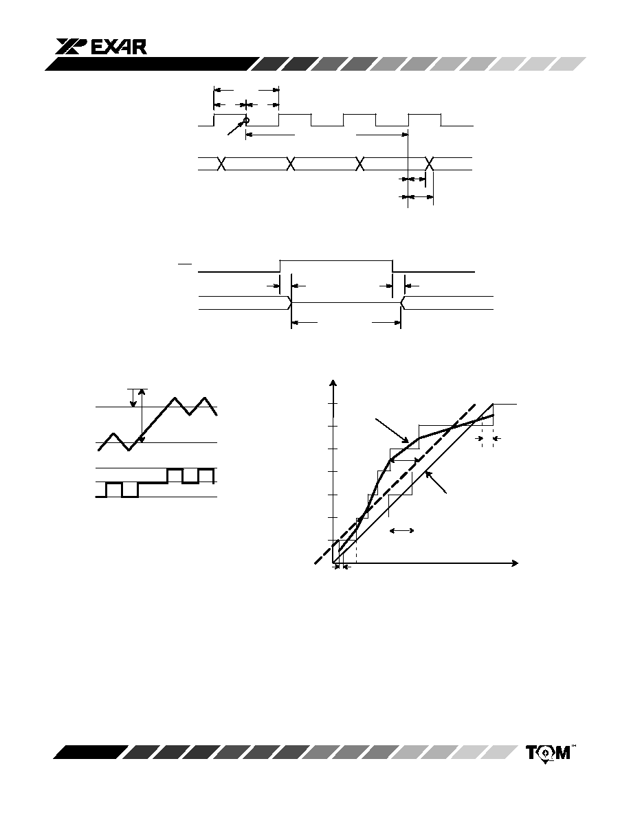
1
Tester measures code transitions by dithering the voltage of the analog input (V
IN
). The difference between the measured and the
ideal code width (V
REF
/256) is the DNL error (
Figure 3.). The INL error is the maximum distance (in LSBs) from the best fit line to
any transition voltage (
Figure 4.). Accuracy is a function of the sampling rate (FS).
2
Guaranteed. Not tested.
3
Specified values guarantee functionality. Refer to other parameters for accuracy.
4
≠1 dB bandwidth is a measure of performance of the A/D input stage (S/H + amplifier). Refer to other parameters for accuracy within
the specified bandwidth.
5
See V
IN
input equivalent circuit (
Figure 5.). Switched capacitor analog input requires driver with low output resistance.
6
All inputs have diodes to DV
DD
and DGND. Input DC currents will not exceed specified limits for any input voltage between
DGND and DV
DD
.
7
t
R
, t
F
should be limited to >5 ns for best results.
8
Depends on the RC load connected to the output pin.
9
AGND & DGND pins are connected through the silicon substrate. Connect together at the package and to the analog ground plane.
Specifications are subject to change without notice
ABSOLUTE MAXIMUM RATINGS (T
A
= +25
∞
C unless otherwise noted)
1, 2, 3
V
DD
to GND
7 V
. . . . . . . . . . . . . . . . . . . . . . . . . . . . . . . . . . . . .
V
RT
& V
RB
V
DD
+0.5 to GND ≠0.5 V
. . . . . . . . . . . . . . . . . . . .
V
IN
V
DD
+0.5 to GND ≠0.5 V
. . . . . . . . . . . . . . . . . . . . . . . . . .
All Inputs
V
DD
+0.5 to GND ≠0.5 V
. . . . . . . . . . . . . . . . . . . . .
All Outputs
V
DD
+0.5 to GND ≠0.5 V
. . . . . . . . . . . . . . . . . . .
Storage Temperature
≠65 to +150
∞
C
. . . . . . . . . . . . . . . . . . .
Lead Temperature (Soldering 10 seconds)
+300
∞
C
. . . . . . .
Package Power Dissipation Rating @ 75
∞
C
PDIP, SOIC
850mW
. . . . . . . . . . . . . . . . . . . . . . . . . . . . . .
Derates above 75
∞
C
12mW/
∞
C
. . . . . . . . . . . . . . . . . . . . .
NOTES:
1
Stresses above those listed under "Absolute Maximum Ratings" may cause permanent damage to the device. This is a
stress rating only and functional operation at or above this specification is not implied. Exposure to maximum rating
conditions for extended periods may affect device reliability.
2
Any input pin which can see a value outside the absolute maximum ratings
should be protected by Schottky diode clamps
(HP5082-2835) from input pin to the supplies.
All inputs have protection diodes which will protect the device from short
transients outside the supplies of less than 100mA for less than 100
µ
s.
3
V
DD
refers to AV
DD
and DV
DD
. GND refers to AGND and DGND.
MP8785
5
Rev. 2.00
CLK
PIPELINE DELAY
N + 1
N + 2
Sample "N"
t
HL
t
DL
N ≠ 3
N ≠ 2
N ≠ 1
DATA N
DATA
High
Impedance
OE
1/FS
t
PWH
t
PWL
t
DHZ
t
DEN
DATA
Figure 1. MP8785 Timing Diagram
Figure 2. Output Enable/Disable Timing Diagram
IDEAL
N + 1
N
N≠1
Output
Codes
Analog
Input
Code Width (N) = V
(
N+1)
≠ V
(
N)
LSB = [
V
RT
≠ V
RB
] / 256
DNL
(N)
= [ V
(N+1)
≠ V
(N)
] ≠ LSB
Figure 3. DNL Measurement
LSB
DNL
7
6
5
4
3
2
1
Output
Codes
Analog Input (Volt)
Figure 4. INL Error Calculation
Best Fit Line
EFS
EZS
LSB
Ideal Transfer Line
Real Transfer Line
INL
V
(N+1)
V
(N)