 | –≠–ª–µ–∫—Ç—Ä–æ–Ω–Ω—ã–π –∫–æ–º–ø–æ–Ω–µ–Ω—Ç: PE-65966 | –°–∫–∞—á–∞—Ç—å:  PDF PDF  ZIP ZIP |
Exar
Corporation 48720 Kato Road, Fremont CA, 94538
∑
(510) 668-7000
∑
FAX (510) 668-7017
∑
www.exar.com
·Á
·Á
·Á
·Á
XRT7300
E3/DS3/STS-1 LINE INTERFACE UNIT
FEBRUARY 2002
REV. 1.1.1
GENERAL DESCRIPTION
The XRT7300 DS3/E3/STS-1 Line Interface Unit is
designed to be used in DS3, E3 or SONET STS-1 ap-
plications and consists of a line transmitter and re-
ceiver integrated on a single chip.
XRT7300 can be configured to support the E3
(34.368 Mbps), DS3 (44.736 Mbps) or the SONET
STS-1 (51.84 Mbps) rates.
In the transmit direction, the XRT7300 encodes input
data to either B3ZS (for DS3/STS-1 applications) or
HDB3 (for E3 applications) format and converts the
data into the appropriate pulse shapes for transmis-
sion over coaxial cable via a 1:1 transformer.
In the receive direction the XRT7300 performs equal-
ization on incoming signals, performs Clock Recov-
ery, decodes data from either B3ZS or HDB3 format,
converts the receive data into TTL/CMOS format,
checks for LOS or LOL conditions and detects and
declares the occurrence of line code violations.
The XRT7300 also contains a 4-Wire Microprocessor
Serial Interface for accessing the on-chip Command
registers.
FEATURES
∑ Meets E3/DS3/STS-1 Jitter Tolerance Require-
ments
∑ Full Loop-Back Capability
∑ Transmit and Receive Power Down Modes
∑ Full Redundancy Support
∑ Contains a 4-Wire Microprocessor Serial Interface
∑ Uses Minimum External components
∑ Requires Single +5V Power Supply
∑ -40∞C to +85∞C Operating Temperature Range
∑ Available in a 44 pin TQFP package
APPLICATIONS
∑ Interfaces to E3, DS3 or SONET STS-1 Networks
∑ CSU/DSU Equipment
∑ PCM Test Equipment
∑ Fiber Optic Terminals
∑ Multiplexers
N
OTE
: This Device is Protected by US Patent # 6,157,270
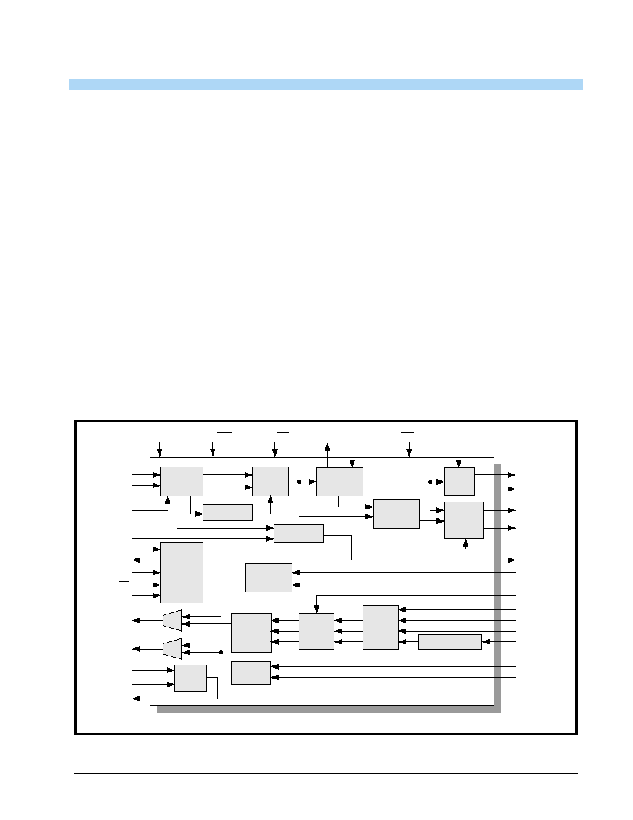
F
IGURE
1. B
LOCK
D
IAGRAM
OF
THE
XRT7300
AGC/
Equalizer
Serial
Processor
Interface
Peak
Detector
LOS Detector
Slicer
Clock
Recovery
Data
Recovery
Invert
Loop MUX
HDB3/
B3ZS
Decoder
LOSTHR
SDI
SDO/(LCV)
SClk
CS
REGRESET
RTIP
RRING
REQDIS
Device
Monitor
MTIP
MRING
DMO
Transmit
Logic
Duty Cycle Adjust
TTIP
TRING
Pulse
Shaping
HDB3/
B3ZS
Encoder
E3
STS-1/DS3
Host/(HW)
RLOL EXCLK
ICT
RCLK2INV
Tx
Control
DECODIS
RLOS
LLB
RLB
ENCODIS
TAOS
TPDATA
TNDATA
TClk
TXLEV
TXOFF
RCLK1
RNEG
RPOS
LCV/(RCLK2)

XRT7300
·Á
·Á
·Á
·Á
E3/DS3/STS-1 LINE INTERFACE UNIT
REV. 1.1.1
2
ORDERING INFORMATION
P
ART
N
UMBER
P
ACKAGE
T
YPE
O
PERATING
T
EMPERATURE
R
ANGE
XRT7300IV
44 Pin TQFP (10mm x 10mm)
-40∞C to +85∞C
F
IGURE
2. P
IN
O
UT
OF
THE
XRT7300
IN
THE
44 P
IN
TQFP
LCV/(RCLK2)
44
43
42
41
40
39
38
37
36
35
34
12
13
14
15
16
17
18
19
20
21
22
23
24
33
32
31
30
29
28
27
26
25
XRT7300
(Top View)
TxLEV
TAOS
VDD
DMO
GND
RTIP
GND
GND
RRING
VDD
REGRESET/
RCLK2INV
REQDIS
LOSTHR
LLB
RLB
STS1/DS3
E3
HOST/HW
SDI/(LOSMUTEN)
SDO/(LCV)
SCLK/(ENCODIS)
CS/(DECODIS)
RPOS
RNEG
RCLK1
VDD
VDD
GND
EXCLK
GND
RLOS
RLOL
MTIP
MRING
VDD
TTIP
TRING
GND
TNDATA
TPDATA
TCLK
TXOFF
ICT
11
10
1
2
3
4
5
6
7
8
9

·Á
·Á
·Á
·Á
E3/DS3/STS-1 LINE INTERFACE UNIT
XRT7300
REV. 1.1.1
I
TABLE OF CONTENTS
General description ........................................................................................................... 1
FEATURES ................................................................................................................................................. 1
APPLICATIONS .......................................................................................................................................... 1
Figure 1.Block Diagram of the XRT7300............................................................................................................ 1
Ordering Information ......................................................................................................... 2
Figure 2.Pin Out of the XRT7300 in the 44 Pin TQFP........................................................................................ 2
TABLE OF CONTENTS ......................................................................................................... I
Pin Description ................................................................................................................... 3
Electrical Characteristics ................................................................................................ 10
DC ELECTRICAL CHARACTERISTICS (TA = 25∞C, VDD = 5.0V + 5%, UNLESS OTHERWISE SPECI-
FIED) ............................................................................................................................................................... 10
AC ELECTRICAL CHARACTERISTICS (TA = 25∞C, VDD = 5.0V + 5%, UNLESS OTHERWISE SPECI-
FIED) ............................................................................................................................................................... 10
Figure 3.Timing Diagram of the Transmit Terminal Input Interface .................................................................. 11
Figure 4.Timing Diagram of the Receive Terminal Output Interface ................................................................ 11
AC ELECTRICAL CHARACTERISTICS (CONTINUED) (TA = 25∞C, VDD = 5.0V + 5%, UNLESS OTHER-
WISE SPECIFIED) .......................................................................................................................................... 12
AC ELECTRICAL CHARACTERISTICS (CONTINUED) (TA = 25∞C, VDD = 5.0V + 5%, UNLESS OTHER-
WISE SPECIFIED) .......................................................................................................................................... 13
ABSOLUTE MAXIMUM RATINGS ..................................................................................... 14
Figure 5.Transmit Pulse Amplitude Test Circuit for DS3, E3 and STS-1 Rates ............................................... 15
Figure 6.ITU-T G.703 Transmit Output Pulse Template for E3 Applications.................................................... 15
Figure 7.Bellcore GR-499-CORE Transmit Output Pulse Template for DS3 Applications............................... 16
Figure 8.Bellcore GR-253-CORE Transmit Output Pulse Template for SONET STS-1 Applications .............. 16
MICROPROCESSOR SERIAL INTERFACE TIMING (SEE FIGURE 9) .................................................. 17
Figure 9.Timing Diagram for the Microprocessor Serial Interface .................................................................... 17
System Description ......................................................................................................... 18
THE TRANSMIT SECTION ....................................................................................................................... 18
THE RECEIVE SECTION ......................................................................................................................... 18
THE MICROPROCESSOR SERIAL INTERFACE .................................................................................... 18
Table 1:Role of Microprocessor Serial Interface pins when the XRT7300 is operating in the Hardware Mode 18
1.0 SELECTING THE DATA RATE ............................................................................................................... 19
Table 2:Selecting the Data Rate for the XRT7300 via the E3 and STS-1/DS3 input pins (Hardware Mode)... 19
COMMAND REGISTER CR4 (ADDRESS = 0X04) .................................................................................. 19
Table 3:Selecting the Data Rate for the XRT7300 Via the STS-1/DS3 and the E3 Bit-fields Within Command
Register CR4 (HOST Mode)................................................................................................................ 19
2.0 THE TRANSMIT SECTION ...................................................................................................................... 20
2.1 T
HE
T
RANSMIT
L
OGIC
B
LOCK
................................................................................................................. 20
Figure 10.The Typical Interface for the Transmission of Data in a Dual-Rail Format From the Transmitting Ter-
minal Equipment to the Transmit Section of the XRT7300 ................................................................ 20
Figure 11.How the XRT7300 Samples the Data on the TPDATA and TNDATA Input Pins ............................. 20
Accepting Single-Rail Data from the Terminal Equipment .................................................................. 21
COMMAND REGISTER CR1 (ADDRESS = 0X01) .................................................................................. 21
Figure 12.The Behavior of the TPDATA and TCLK Input Signals While the Transmit Logic Block is Accepting
Single-Rail Data From the Terminal Equipment................................................................................. 21

XRT7300
E3/DS3/STS-1 LINE INTERFACE UNIT
·Á
·Á
·Á
·Á
REV. 1.1.1
II
2.2 T
HE
T
RANSMIT
C
LOCK
D
UTY
C
YCLE
A
DJUST
C
IRCUITRY
......................................................................... 21
2.3 T
HE
HDB3/B3ZS E
NCODER
B
LOCK
........................................................................................................ 22
B3ZS Encoding .................................................................................................................................... 22
Figure 13.An Example of B3ZS Encoding ........................................................................................................ 22
HDB3 Encoding.................................................................................................................................... 22
Figure 14.An Example of HDB3 Encoding ........................................................................................................ 23
Enabling/Disabling the HDB3/B3ZS Encoder ...................................................................................... 23
2.4 T
HE
T
RANSMIT
P
ULSE
S
HAPER
C
IRCUITRY
.............................................................................................. 23
COMMAND REGISTER CR2 (ADDRESS = 0X02 .................................................................................... 23
Enabling the Transmit Line Build-Out Circuit ....................................................................................... 23
Disabling the Transmit Line Build-Out Circuit ...................................................................................... 23
COMMAND REGISTER CR1 (ADDRESS = 0X01) ................................................................................... 23
Design Guideline for Setting the Transmit Line Build-Out Circuit ........................................................ 24
COMMAND REGISTER CR1 (ADDRESS = 0X01) ................................................................................... 24
The Transmit Line Build-Out Circuit and E3 Applications .................................................................... 24
2.5 I
NTERFACING
THE
T
RANSMIT
S
ECTION
OF
THE
XRT7300
TO
THE
L
INE
..................................................... 24
Figure 15.Recommended Schematic for Interfacing the Transmit Section of the XRT7300 to the Line...........24
TRANSFORMER RECOMMENDATIONS ........................................................................................................ 25
3.0 THE RECEIVE SECTION ......................................................................................................................... 25
3.1 I
NTERFACING
THE
R
ECEIVE
S
ECTION
OF
THE
XRT7300
TO
THE
L
INE
....................................................... 25
Figure 16.Recommended Schematic for Interfacing the Receive Section of the XRT7300 to the Line (Transform-
er-Coupling) ........................................................................................................................................ 26
Figure 17.Recommended Schematic for Interfacing the Receive Section of the XRT7300 to the Line (Capaci-
tive-Coupling)...................................................................................................................................... 26
3.2 T
HE
R
ECEIVE
E
QUALIZER
B
LOCK
............................................................................................................26
Figure 18. The Typical Application for the System Installer .............................................................................. 27
COMMAND REGISTER CR2 (ADDRESS = 0X02) ................................................................................... 28
3.3 P
EAK
D
ETECTOR
AND
S
LICER
................................................................................................................. 28
3.4 C
LOCK
R
ECOVERY
PLL .......................................................................................................................... 28
3.5 T
HE
HDB3/B3ZS D
ECODER
...................................................................................................................28
B3ZS Decoding DS3/STS-1 Applications ............................................................................................ 29
Figure 19.An Example of B3ZS Decoding ........................................................................................................ 29
HDB3 Decoding E3 Applications.......................................................................................................... 29
Figure 20.An Example of HDB3 Decoding........................................................................................................ 29
Enabling/Disabling the HDB3/B3ZS Decoder ...................................................................................... 30
3.6 LOS D
ECLARATION
/C
LEARANCE
............................................................................................................. 30
COMMAND REGISTER CR2 (ADDRESS = 0X02) ................................................................................... 30
The LOS Declaration/Clearance Criteria for E3 Applications...............................................................30
Figure 21.The Signal Levels that the XRT7300 Declares and Clears LOS (E3 Mode Only) ............................ 31
Figure 22.The Behavior the LOS Output Indicator In Response to the Loss of Signal and the Restoration of Sig-
nal ....................................................................................................................................................... 31
The LOS Declaration/Clearance Criteria for DS3 and STS-1 Applications.......................................... 32
Table 4:The ALOS Declaration and Clearance Thresholds for a Given Setting of LOSTHR (DS3 and STS-1 Ap-
plications) for Equalizer Enabled or Disabled ...................................................................................... 32
COMMAND REGISTER CR0 (ADDRESS = 0X00) ................................................................................... 32
COMMAND REGISTER CR2 (ADDRESS = 0X02) ................................................................................... 33
COMMAND REGISTER CR0 (ADDRESS = 0X00) ................................................................................... 33

·Á
·Á
·Á
·Á
E3/DS3/STS-1 LINE INTERFACE UNIT
XRT7300
REV. 1.1.1
III
COMMAND REGISTER CR2 (ADDRESS = 0X02) .................................................................................. 33
Muting the Recovered Data while the LOS is being Declared............................................................. 33
3.7 R
OUTING
THE
R
ECOVERED
T
IMING
AND
D
ATA
I
NFORMATION
TO
THE
R
ECEIVING
T
ERMINAL
E
QUIPMENT
.... 33
COMMAND REGISTER CR3 (ADDRESS = 0X03) .................................................................................. 33
Figure 23. The Typical Interface for the Transmission of Data in a Dual-Rail Format From the Receive Section
of the XRT7300 to the Receiving Terminal Equipment ...................................................................... 34
Figure 24. How the XRT7300 Outputs Data on the RPOS and RNEG Output Pins ........................................ 34
Figure 25.The Behavior of the RPOS, RNEG and RCLK1 Signals When RCLK1 is Inverted ......................... 35
Routing Single-Rail Format data (Binary Data Stream) to the Receive Terminal Equipment ............. 35
COMMAND REGISTER CR3 (ADDRESS = 0X03) .................................................................................. 35
COMMAND REGISTER CR3 (ADDRESS = 0X03) .................................................................................. 35
Figure 26.The Typical Interface for the Transmission of Data in a Single-Rail Format From the Receive Section
of the XRT7300 to the Receiving Terminal Equipment ...................................................................... 36
Figure 27.The Behavior of the RPOS and RCLK1 Output Signals While the XRT7300 is Transmitting Single-Rail
Data to the Receiving Terminal Equipment........................................................................................ 36
4.0 DIAGNOSTIC FEATURES OF THE XRT7300 ........................................................................................ 36
4.1 T
HE
A
NALOG
L
OCAL
L
OOP
-B
ACK
M
ODE
................................................................................................. 36
Figure 28.The Analog Local Loop-Back in the XRT7300 ................................................................................. 37
COMMAND REGISTER CR4 (ADDRESS = 0X04) .................................................................................. 37
4.2 T
HE
D
IGITAL
L
OCAL
L
OOP
-B
ACK
M
ODE
.................................................................................................. 37
Figure 29.The Digital Local Loop-Back path in the XRT7300 .......................................................................... 38
COMMAND REGISTER CR4 (ADDRESS = 0X04) .................................................................................. 38
4.3 T
HE
R
EMOTE
L
OOP
-B
ACK
M
ODE
............................................................................................................ 38
Figure 30.The Remote Loop-Back Path in the XRT7300 ................................................................................. 39
COMMAND REGISTER CR4 (ADDRESS = 0X04) .................................................................................. 39
4.4 TXOFF F
EATURES
................................................................................................................................. 40
COMMAND REGISTER CR1 (ADDRESS = 0X01) .................................................................................. 40
4.5 T
HE
T
RANSMIT
D
RIVE
M
ONITOR
F
EATURES
............................................................................................ 40
Figure 31.The XRT7300 Employing the Transmit Drive Monitor Features....................................................... 40
Figure 32. Two LIU's, Each Monitoring the Transmit Output Signal of the Other LIU IC ................................. 41
4.6 T
HE
TAOS (T
RANSMIT
A
LL
O
NE
S) F
EATURE
.......................................................................................... 41
COMMAND REGISTER CR1 (ADDRESS = 0X01) .................................................................................. 41
5.0 THE MICROPROCESSOR SERIAL INTERFACE ................................................................................... 42
5.1 D
ESCRIPTION
OF
THE
C
OMMAND
R
EGISTERS
.......................................................................................... 42
Table 5:Addresses and Bit Formats of XRT7300 Command Registers ........................................................... 42
DESCRIPTION OF BIT-FIELDS FOR EACH COMMAND REGISTER .................................................... 42
Command Register - CR0 ................................................................................................................... 42
Command Register - CR1 ................................................................................................................... 43
Command Register - CR2 ................................................................................................................... 44
Command Register - CR3 ................................................................................................................... 44
Command Register - CR4 ................................................................................................................... 45
5.2 O
PERATING
THE
M
ICROPROCESSOR
S
ERIAL
I
NTERFACE
. ......................................................................... 45
Table 6:Loop-Back Modes................................................................................................................................ 45
Figure 33.Microprocessor Serial Interface Data Structure ............................................................................... 46
Figure 34. How to Interface the XRT7300 IC to the XRT7234/45 E3/DS3 ATM UNI IC .................................. 47
Figure 35.How to Interface the XRT7300 IC to the XRT7250 DS3/E3 Framer IC............................................ 48
ORDERING INFORMATION ..................................................................................................................... 49
Package Dimensions ....................................................................................................... 49

XRT7300
E3/DS3/STS-1 LINE INTERFACE UNIT
·Á
·Á
·Á
·Á
REV. 1.1.1
IV
REVISION HISTORY ................................................................................................................................ 50

·Á
·Á
·Á
·Á
XRT7300
E3/DS3/STS-1 LINE INTERFACE UNIT
REV. 1.1.1
3
PIN DESCRIPTION
PIN DESCRIPTION
P
IN
#
S
YMBOL
T
YPE
D
ESCRIPTION
1
TXLEV
I
Transmit Line Build-Out Enable/Disable Select:
This input pin is used to enable or disable the Transmit Line Build-Out circuit in
the XRT7300.
Setting this pin to "High" disables the Line Build-Out circuit. In this mode, the
XRT7300 outputs partially shaped pulses onto the line via the TTIP and TRING
output pins.
Setting this pin to "Low" enables the Line Build-Out circuit. In this mode, the
XRT7300 outputs partially-shaped pulses onto the line via the TTIP and TRING
output pins.
To comply with the isolated DSX-3/STSX-1 Pulse Template Requirements per
Bellcore GR-499-Core or Bellcore GR-253-Core:
1. Set this input pin to a "1" if the cable length between the Cross-Connect and
the transmit output of the XRT7300 is greater than 225 feet.
2. Set this input pin to a "0" if the cable length between the Cross-Connect and
the transmit output of the XRT7300 is less than 225 feet.
This pin is active only if both of the following are true:
(a) The XRT7300 is configured to operate in either the DS3 or SONET STS-1
modes and
(b) The XRT7300 is configured to operate in the Hardware Mode.
N
OTE
: This pin should be tied to GND if the XRT7300 is to be operated in the
HOST mode.
2
TAOS
I
Transmit All Ones Select:
A "High" on this pin causes a continuous AMI all "1's" pattern to be transmitted
onto the line. The frequency of this "1's" pattern is determined by TCLK.
N
OTES
:
1. This input pin is ignored if the XRT7300 is operating in the HOST Mode.
2. Tie this pin to GND if the XRT7300 is going to be operating in the HOST
Mode.
3
VDD
****
Transmit Digital Power Supply
4
DMO
O
Drive Monitor Output:
If no transmitted AMI signal is present on MTIP and MRING input pins for
128±32 TCLK periods, then the DMO pin toggles and remains "High" until the
next AMI signal is detected.
5
GND
****
Transmit Digital GND
6
GND
****
Analog GND (Substrate)
7
GND
****
Receive Analog GND
8
RTIP
I
Receive TIP Input:
This input pin along with RRING is used to receive the line signal from the
Remote DS3/E3/STS-1 Terminal.
9
RRING
I
Receive RING Input:
This input pin along with RTIP is used to receive the line signal from the Remote
DS3/E3/STS-1 Terminal.
10
VDD
****
Receive Analog VDD

XRT7300
·Á
·Á
·Á
·Á
E3/DS3/STS-1 LINE INTERFACE UNIT
REV. 1.1.1
4
11
REGRESET/
(RCLK2INV)
I
Register Reset Input pin (Invert RCLK2 Output - Select):
The function of this pin depends upon whether the XRT7300 is operating in the
HOST Mode or in the Hardware Mode.
HOST Mode - Register Reset Input pin:
Setting this input pin "Low" causes the XRT7300 to reset the contents of the
Command Registers to their default settings and operating configuration. This
pin is internally pulled "High".
Hardware Mode - Invert RCLK2 Output Select:
Setting this input pin "Low" configures the Receive Section of the XRT7300 to
output the recovered data via the RPOS and RNEG output pins on the rising
edge of the RCLK2 output signal.
Setting this input pin "High" configures the Receive Section to output the recov-
ered data on the falling edge of the RCLK2 output signal.
12
REQDIS
I
Receive Equalization Disable Input:
Setting this input pin "High" disables the Internal Receive Equalizer in the
XRT7300. Setting this pin "Low" enables the Internal Receive Equalizer. The
guidelines for enabling and disabling the Receive Equalizer are described in
Section 3.2.
N
OTES
:
1. This input pin is ignored if the XRT7300 is operating in the HOST Mode.
2. Tie this pin to GND if the XRT7300 is going to be operating in the HOST
Mode.
13
LOSTHR
I
Loss of Signal Threshold Control:
The voltage forced on this pin controls the input loss of signal (LOS) threshold.
Two settings are provided by forcing this signal to either GND or VDD.
N
OTE
: This pin is only applicable during DS3 or STS-1 operations.
14
LLB
I
Local Loop-Back Select:
This input pin along with RLB dictates which Loop-Back mode the XRT7300 is
operating in.
A "High" on this pin with RLB being set to "Low" configures the XRT7300 to oper-
ate in the Analog Local Loop-Back Mode.
A "High" on this pin with RLB also being set to "High" configures the XRT7300 to
operate in the Digital Local Loop-Back Mode.
N
OTES
:
1. This input pin is ignored if the XRT7300 is operating in the HOST Mode.
2. Tie this pin to GND if the XRT7300 is going to be operating in the HOST
Mode.
15
RLB
I
Remote Loop-Back Select:
This input pin along with LLB dictates which Loop-Back mode the XRT7300 is be
operating in.
A "High" on this pin with LLB being set to "Low" configures the XRT7300 to oper-
ate in the Remote Loop-Back Mode.
A "High" on this pin with LLB also being set to "High" configures the XRT7300 to
operate in the Digital Local Loop-Back Mode.
N
OTES
:
1. This input pin is ignored if the XRT7300 is operating in the HOST Mode.
2. Tie this pin to GND if the XRT7300 is going to be operating in the HOST
Mode.
PIN DESCRIPTION
P
IN
#
S
YMBOL
T
YPE
D
ESCRIPTION

·Á
·Á
·Á
·Á
XRT7300
E3/DS3/STS-1 LINE INTERFACE UNIT
REV. 1.1.1
5
16
STS-1/DS3
I
STS-1/DS3 Select Input:
A "High" on this pin configures the Clock Recovery Phase Locked Loop to set its
VCO Center frequency to around 51.84 MHz (optimal for SONET STS-1 opera-
tions). A "Low" on this pin configures the Clock Recovery Phase Locked Loop to
set its VCO Center frequency to around 44.736 MHz (optimal for DS3 opera-
tions).
N
OTES
:
1. The XRT7300 ignores this pin if the E3 pin (pin 17) is set to "1".
2. This input pin is ignored if the XRT7300 is operating in the HOST Mode.
3. Tie this pin to GND if the XRT7300 is going to be operating in the HOST
Mode.
17
E3
I
E3 Select Input:
A "High" on this pin configures the XRT7300 to operate in the E3 Mode.
A "Low" on this pin configures the XRT7300 to check the state of the STS-1/DS3
input pin.
N
OTES
:
1. This input pin is ignored if the XRT7300 is operating in the HOST Mode.
2. Tie this pin to GND if the XRT7300 is going to be operating in the HOST
Mode.
18
HOST/HW
I
HOST/HW Mode Select:
This input pin is used to enable or disable the Microprocessor Serial Interface
(e.g., consisting of the SDI, SDO, SCLK, CS and REGRESET pins).
Setting this input pin "High" enables the Microprocessor Serial Interface (e.g.
configures the XRT7300 to operate in the HOST Mode). In this mode, the
XRT7300 is configured by writing data into the on-chip Command Registers via
the Microprocessor Serial Interface. When the XRT7300 is operating in the
HOST Mode, it ignores the states of many of the discrete input pins.
Setting this input pin "Low" disables the Microprocessor Serial Interface (e.g.,
configures the XRT7300 to operate in the Hardware Mode). In this mode, many
of the external input control pins are functional.
19
SDI/
(LOSMUTEN)
I
Serial Data Input for the Microprocessor Serial Interface (HOST Mode) or
MUTE-upon-LOS Enable Input (Hardware Mode):
The function of this input pin depends upon whether the XRT7300 is operating in
the HOST or the Hardware Mode.
Serial Data Input for the Microprocessor Serial Interface (HOST Mode):
This pin is used to read or write data into the Command Registers of the Micro-
processor Serial Interface. The Read/Write bit, the Address Values of the Com-
mand Registers and Data Value to be written during Write Operations are
applied to this pin.
This input is sampled on the rising edge of the SCLK pin (pin 21).
MUTE-upon-LOS Enable Input (Hardware Mode):
When in the Hardware Mode, this input pin is used to configure the XRT7300 to
MUTE the recovered data via the RPOS and RNEG output pins whenever it
declares an LOS condition.
Setting this input pin "High" configures the XRT7300 to automatically pull the
RPOS and RNEG output pins to GND whenever it is declaring an LOS condition,
thereby MUTing the data being output to the Terminal Equipment.
Setting this input pin "Low" configures the XRT7300 to NOT automatically MUTE
the recovered data whenever an LOS condition is declared.
PIN DESCRIPTION
P
IN
#
S
YMBOL
T
YPE
D
ESCRIPTION

XRT7300
·Á
·Á
·Á
·Á
E3/DS3/STS-1 LINE INTERFACE UNIT
REV. 1.1.1
6
20
SDO/(LCV)
O
Serial Data Output from the Controller Port/(Line Code Violation Output
(LCV) Indicator.):
The function of this input pin depends upon whether the XRT7300 is operating in
the HOST or the Hardware Mode.
HOST Mode - Microprocessor Serial Interface - Serial Data Output.
This pin serially outputs the contents of the specified Command Register during
Read Operations. The data on this pin is updated on the falling edge of the
SCLK input signal. This pin is tri-stated upon completion of data transfer.
Hardware Mode - Line Code Violation Output Indicator.
This pin pulses "High" for one bit period any time the Receive Section of the
XRT7300 detects a Line Code Violation in the incoming E3, DS3 or STS-1 Data
Stream.
21
SCLK/(ENCO-
DIS)
I
Microprocessor Serial Interface Clock Signal/Encoder Disable:
HOST Mode - Microprocessor Serial Interface Clock Signal
This signal is used to sample the data on the SDI pin on the rising edge of this
signal. Additionally, during Read operations the Microprocessor Serial Interface
updates the SDO output on the falling edge of this signal.
Hardware Mode - B3ZS/HDB3 Encoder Disable
Setting this input pin "High" disables the B3ZS/HDB3 Encoder and configures
the XRT7300 to transmit the line signal in an AMI Format.
Setting this input pin "Low" enables the B3ZS/HDB3 Encoder and configures the
XRT7300 to transmit the line signal in the B3ZS format (for DS3/STS-1 opera-
tion) or in the HDB3 format (for E3 operation).
22
CS/(DECODIS)
I
Microprocessor Serial Interface - Chip Select/Decoder Disable
The function of this input pin depends upon whether the XRT7300 is operating in
the HOST or the Hardware Mode.
HOST Mode - Chip Select Input:
The Local Microprocessor must assert this pin (e.g., set it to "0") in order to
enable communication with the XRT7300 via the Microprocessor Serial Inter-
face.
Hardware Mode - (B3ZS/HDB3 Decoder Disable)
Setting this input pin "High" disables the B3ZS/HDB3 Decoder. Setting this input
pin "Low" enables the B3ZS/HDB3 Decoder.
23
RLOL
O
Receive Loss of Lock Output Indicator
This output pin toggles "High" if the XRT7300 has detected a Loss of Lock Con-
dition. The XRT7300 declares an LOL (Loss of Lock) Condition if the recovered
clock frequency deviates from the Reference Clock frequency (available at the
EXCLK input pin) by more than 0.5%.
24
RLOS
O
Receive Loss of Signal Output Indicator
This output pin toggles "High" if the XRT7300 has detected a Loss of Signal
Condition in the incoming line signal.
The criteria the XRT7300 uses to declare an LOS Condition depends upon
whether the device is operating in the E3 or DS3/STS-1 Mode.
25
GND ****
Digital GND
26
VDD
****
Digital VDD
PIN DESCRIPTION
P
IN
#
S
YMBOL
T
YPE
D
ESCRIPTION

·Á
·Á
·Á
·Á
XRT7300
E3/DS3/STS-1 LINE INTERFACE UNIT
REV. 1.1.1
7
27
EXCLK
I
External Reference Clock Input:
Apply a 34.368MHz clock signal for E3 applications, a 44.736 MHz clock signal
for DS3 applications or a 51.84 MHz clock signal for SONET STS-1 applications.
28
GND
****
Receiver Digital Ground
29
VDD
****
Receiver Digital VDD
30
LCV/(RCLK2)
O
Line Code Violation Indicator/Receive Clock Output pin 2:
The function of this pin depends upon whether the XRT7300 is operating in the
HOST Mode, the Hardware Mode or User selection.
HOST Mode - Line Code Violation Indicator Output:
If the XRT7300 is configured to operate in the HOST Mode, then this pin func-
tions as the LCV output pin by default. However, by using the on-chip Command
Registers, this pin can be configured to function as the second Receive Clock
signal output pin (RCLK2).
Hardware Mode - Receive Clock Output pin 2:
This output pin is the Recovered Clock signal from the incoming line signal. The
receive section of the XRT7300 outputs data via the RPOS and RNEG output
pins on the rising edge of this clock signal.
N
OTE
: If the XRT7300 is operating in the HOST Mode and this pin is configured
to function as the additional Receive Clock signal output pin, then the XRT7300
can be configured to update the data on the RPOS and RNEG output pins on the
falling edge of this clock signal.
31
RCLK1
O
Receive Clock Output pin 1:
This output pin is the Recovered Clock signal from the incoming line signal. The
receive section of the XRT7300 outputs data via the RPOS and RNEG output
pins on the rising edge of this clock signal.
N
OTE
: If the XRT7300 device is operating in the "Host" Mode, then the user can
configure the device to update the data on the RPOS and RNEG output pins on
the falling edge of this clock signal.
32
RNEG
O
Receive Negative Pulse Output:
This output pin pulses "High" whenever the XRT7300 has received a Negative
Polarity pulse in the incoming line signal at the RTIP/RRING inputs.
N
OTE
: If the B3ZS/HDB3 Decoder is enabled, then the zero suppression pat-
terns in the incoming line signal (such as: "00V", "000V", "B0V", "B00V") is not
reflected at this output.
33
RPOS
O
Receive Positive Pulse Output:
This output pin pulses "High" whenever the XRT7300 has received a Positive
Polarity pulse in the incoming line signal at the RTIP/RRING inputs.
N
OTE
: If the B3ZS/HDB3 Decoder is enabled, then the zero suppression pat-
terns in the incoming line signal (such as: "00V", "000V", "B0V", "B00V") is not
reflected at this output.
34
ICT
I
In-Circuit Test Input:
Setting this pin "Low" causes all digital and analog outputs to go into a high-
impedance state to allow for in-circuit testing. This pin is internally pulled "High".
PIN DESCRIPTION
P
IN
#
S
YMBOL
T
YPE
D
ESCRIPTION

XRT7300
·Á
·Á
·Á
·Á
E3/DS3/STS-1 LINE INTERFACE UNIT
REV. 1.1.1
8
35
TXOFF
I
Transmitter OFF Input:
Setting this input pin "High" configures the XRT7300 to turn off the Transmitter in
the device.
N
OTES
:
1. This input pin is ignored if the XRT7300 is operating in the HOST Mode.
2. Tie this pin to GND if the XRT7300 is going to be operating in the HOST
Mode.
36
TCLK
I
Transmit Clock Input for TPDATA and TNDATA:
This input pin must be driven at 34.368 MHz for E3 applications, 44.736MHz for
DS3 applications, or 51.84MHz for SONET STS-1 applications. The XRT7300
uses this signal to sample the TPDATA and TNDATA input pins. By default, the
XRT7300 is configured to sample these two pins on the falling edge of this sig-
nal.
If the XRT7300 is operating in the HOST Mode, then the device can be config-
ured to sample the TPDATA and TNDATA input pins on the rising edge of TCLK.
37
TPDATA
I
Transmit Positive Data Input:
The XRT73L00 samples this pin on the falling edge of TCLK. If the device sam-
ples a "1" at this input pin, then it generates and transmits a positive polarity
pulse to the line.
N
OTES
:
1. The data should be applied to this input pin if the Transmit Section is
configured to accept Single-Rail data from the Terminal Equipment.
2. If the XRT73L00 is operating in the HOST Mode, then the XRT73L00
can be configured to sample the TPDATA pin on either the rising or fall-
ing edge of TCLK.
38
TNDATA
I
Transmit Negative Data Input:
The XRT7300 samples this pin on the falling edge of TCLK. If the device sam-
ples a "1" at this input pin, then it generates and transmits a negative polarity
pulse to the line.
N
OTES
:
1. This input pin is ignored and should be tied to GND if the Transmit Sec-
tion is configured to accept Single-Rail data from the Terminal Equip-
ment.
2. If the XRT7300 is operating in the HOST Mode, then the XRT7300 can
be configured to sample the TNDATA pin on either the rising or falling
edge of TCLK.
39
GND
-
Transmit Analog Ground
40
TRING
O
Transmit TIP Output:
The XRT7300 uses this pin, along with TTIP, to transmit a bipolar line signal via a
1:1 transformer.
41
TTIP
O
Transmit RING Output:
The XRT7300 uses this pin, along with TRING, to transmit a bipolar line signal
via a 1:1 transformer.
42
VDD
-
Transmit Analog Power Supply
PIN DESCRIPTION
P
IN
#
S
YMBOL
T
YPE
D
ESCRIPTION

·Á
·Á
·Á
·Á
XRT7300
E3/DS3/STS-1 LINE INTERFACE UNIT
REV. 1.1.1
9
43
MRING
I
Monitor Ring Input:
The bipolar line output signal from TRING can be connected to this pin via a 270
resistor in order to check for line driver failure. This pin is internally pulled
"High".
44
MTIP
I
Monitor Tip Input:
The bipolar line output signal from TTIP can be connected to this pin via a 270
resistor in order to check for line driver failure. This pin is internally pulled "High".
PIN DESCRIPTION
P
IN
#
S
YMBOL
T
YPE
D
ESCRIPTION

XRT7300
·Á
·Á
·Á
·Á
E3/DS3/STS-1 LINE INTERFACE UNIT
REV. 1.1.1
10
ELECTRICAL CHARACTERISTICS
* Not applicable to pins with pull-up/pull-down resistors.
DC ELECTRICAL CHARACTERISTICS (T
A
= 25
∞
C, V
DD
= 5.0V + 5%,
UNLESS
OTHERWISE
SPECIFIED
)
S
YMBOL
P
ARAMETER
M
IN
.
T
YP
.
M
AX
.
U
NITS
V
DDD
DC Supply Voltage
4.75
5
5.25
V
V
DDA
DC Supply Voltage
4.75
5
5.25
V
I
CC
Supply Current (Measured while Transmitting and Receiving all "1's")
DS-3 Mode
167
200
mA
STS-1 Mode
180
220
mA
V
IL
Input Low Voltage
0.8
V
V
IH
Input High Voltage
2.0
VDD
V
V
OL
Output Low Voltage, IOUT = -4.0mA
0
0.4
V
V
OH
Output High Voltage, IOUT = 4.0mA
2.8
VDD
V
I
L
Input Leakage Current*
±10
mA
AC ELECTRICAL CHARACTERISTICS (T
A
= 25
∞
C, V
DD
= 5.0V + 5%,
UNLESS
OTHERWISE
SPECIFIED
)
S
YMBOL
P
ARAMETER
M
IN
.
T
YP
.
M
AX
.
U
NITS
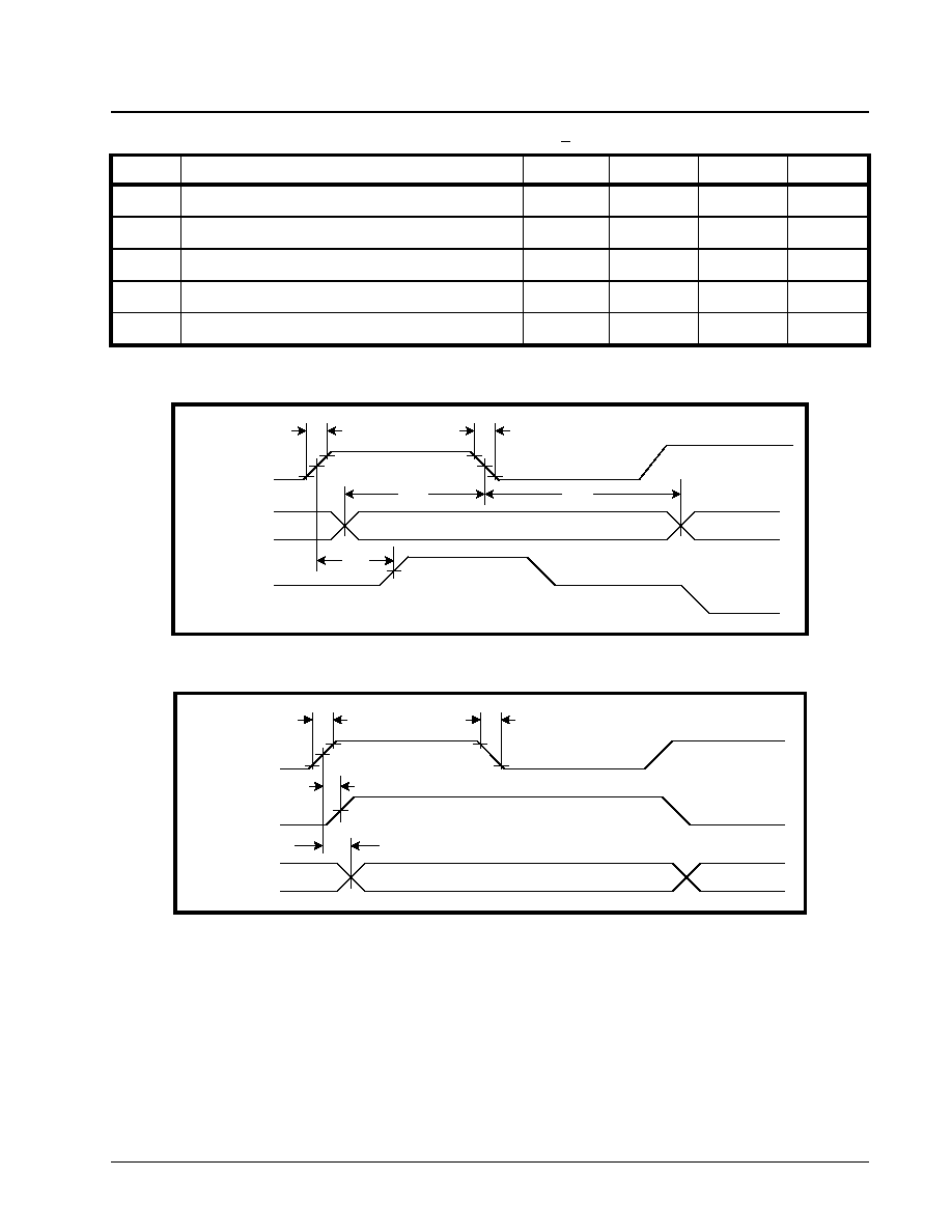
Terminal Side Timing Parameters (See Figure 3 & Figure 4)
TCLK Clock Duty Cycle (DS3/STS-1)
30
50
70
%
TCLK Clock Duty Cycle (E3)
30
50
70
%
TCLK Frequency (SONET STS-1)
51.84
MHz
TCLK Frequency (DS3)
44.736
MHz
TCLK Frequency (E3)
34.368
MHz
t
RTX
TCLK Clock Rise Time (10% to 90%)
4
ns
t
FTX
TCLK Clock Fall Time (90% to 10%)
4
ns
t
TSU
TPDATA/TNDATA to TCLK Falling Set up time
3
ns
t
THO
TPDATA/TNDATA to TCLK Falling Hold time
3
ns
t
LCVO
RCLK to rising edge of LCV output delay
2.5
ns
t
TDY
TTIP/TRING to TCLK Rising Propagation Delay time
0.6
14
ns
RCLK Clock Duty Cycle
45
50
55
%
RCLK Frequency (SONET STS-1)
51.84
MHz
RCLK Frequency (DS3)
44.736
MHz
RCLK Frequency (E3)
34.368
MHz
·Á
·Á
·Á
·Á
XRT7300
E3/DS3/STS-1 LINE INTERFACE UNIT
REV. 1.1.1
11
t
CO
RCLK to RPOS/RNEG Delay Time
4
ns
t
RRX
RCLK Clock Rise Time (10% to 90%)
2
4
ns
t
FRX
RCLK Clock Fall Time (10% to 90%)
1.5
3
ns
C
i
Input Capacitance
10
pF
C
L
Load Capacitance
10
pF
AC ELECTRICAL CHARACTERISTICS (T
A
= 25
∞
C, V
DD
= 5.0V + 5%,
UNLESS
OTHERWISE
SPECIFIED
)
S
YMBOL
P
ARAMETER
M
IN
.
T
YP
.
M
AX
.
U
NITS
F
IGURE
3. T
IMING
D
IAGRAM
OF
THE
T
RANSMIT
T
ERMINAL
I
NPUT
I
NTERFACE
T P D A T A o r
T N D A T A
TTIP or
T R I N G
TClk
t
T S U
t
T H O
t
R T X
t
F T X
t
T D Y
F
IGURE
4. T
IMING
D
IAGRAM
OF
THE
R
ECEIVE
T
ERMINAL
O
UTPUT
I
NTERFACE
R C l k
t
R R X
t
F R X
R P O S o r
R N E G
L C V
t
L C V O
t
C O

XRT7300
·Á
·Á
·Á
·Á
E3/DS3/STS-1 LINE INTERFACE UNIT
REV. 1.1.1
12
(1) Measured at Nominal DSX3 level, Equalizer enabled,
VDD = 5V and TA = 25
o
C
AC ELECTRICAL CHARACTERISTICS (CONTINUED) (TA = 25
∞
C, VDD = 5.0V + 5%, UNLESS OTHER-
WISE SPECIFIED)
Line Side Parameters
S
YMBOL
P
ARAMETER
M
IN
.
T
YP
.
M
AX
.
U
NITS
DS3 Application Parameters
Transmit Line Characteristics (See Figure 5)
Transmit Output Pulse Amplitude (Measured at 0 feet, TXLEV = 0)
0.68
0.75
0.85
Vpk
Transmit Output Pulse Amplitude (Measured at 0 feet, TXLEV = 1)
0.90
1.0
1.1
Vpk
Transmit Output Pulse Width
10.10
11.18
12.28
ns
Transmit Output Pulse Amplitude Ratio
0.9
1.0
1.1
Transmit Output Jitter with jitter-free input clock at TCLK
0.02
0.05
UIpp
Receive Line Characteristics
Receive Sensitivity (Length of Cable)
900
1000
feet
Receive Intrinsic Jitter (All One's Pattern)
0.01
UI
Receive Intrinsic Jitter (100 Pattern)
(1)
0.02
UI
LOS Level With Equalizer Enabled (Table 4)
Signal Level to Declare Loss of Signal (LOSTHR = 0)
55
mV
Signal Level to Clear Loss of Signal (LOSTHR = 0)
220
mV
Signal Level to Declare Loss of Signal (LOSTHR = 1)
22
mV
Signal Level to Clear Loss of Signal (LOSTHR = 1)
90
mV
LOS Level With Equalizer Disabled (Table 4)
Signal Level to Declare Loss of Signal (LOSTHR = 0)
35
mV
Signal Level to Clear Loss of Signal (LOSTHR = 0)
155
mV
Signal Level to Declare Loss of Signal (LOSTHR = 1)
17
mV
Signal Level to Clear Loss of Signal (LOSTHR = 1)
70
mV
Max Jitter Tolerance @ Jitter Frequency = 100Hz
64
UI
Max Jitter Tolerance @ Jitter Frequency = 1KHz
64
UI
Max Jitter Tolerance @ Jitter Frequency = 10KHz
5
UI
Max Jitter Tolerance @ Jitter Frequency = 800KHz
0.4
UI

·Á
·Á
·Á
·Á
XRT7300
E3/DS3/STS-1 LINE INTERFACE UNIT
REV. 1.1.1
13
AC ELECTRICAL CHARACTERISTICS (CONTINUED) (TA = 25
∞
C, VDD = 5.0V + 5%, UNLESS OTHER-
WISE SPECIFIED)
Line Side Parameters
S
YMBOL
P
ARAMETER
M
IN
.
T
YP
.
M
AX
.
U
NITS
E3 Application Parameters
Transmit Line Characteristics (See Figure 5)
Transmit Output Pulse Amplitude (Measured at Secondary Out-
put of Transformer)
0.9
1.00
1.1
Vpk
Transmit Output Pulse Amplitude Ratio
0.95
1.00
1.05
Transmit Output Pulse Width
12.5
14.55
16.5
ns
Transmit Output Pulse Width Ratio
0.95
1.00
1.05
Transmit Output Jitter with jitter-free input clock at TCLK
0.02
0.05
UIpp
Receive Line Characteristics
Receive Sensitivity (Length of cable)
1100
feet
Interference Margin
-20
-17
dB
Signal Level to Declare Loss of Signal
-35
dB
Signal Level to Clear Loss of Signal
-15
dB
Occurrence of LOS to LOS Declaration Time
10
100
255
UI
Termination of LOS to LOS Clearance Time
10
100
255
UI
Intrinsic Jitter (all "1's" Pattern)
(1)
0.01
UI
Intrinsic Jitter (100 Pattern)
0.03
Max Jitter Tolerance @ Jitter Frequency = 100Hz
64
UI
Max Jitter Tolerance @ Jitter Frequency = 1KHz
30
UI
Max Jitter Tolerance @ Jitter Frequency = 10KHz
4
UI
Max Jitter Tolerance @ Jitter Frequency = 800KHz
0.15
UI
SONET STS-1 Application Parameters
Transmit Line Characteristics (See Figure 5)
Transmit Output Pulse Amplitude (Measured with TXLEV = 0)
0.68
0.75
0.85
Vpk
Transmit Output Pulse Amplitude (Measured with TXLEV = 1)
0.93
0.98
1.08
Vpk
Transmit Output Pulse Width
8.6
9.65
10.6
ns
Transmit Output Pulse Amplitude Ratio
0.9
1.0
1.1
Transmit Output Jitter with jitter-free clock input at TCLK
0.02
0.05
UIpp

XRT7300
·Á
·Á
·Á
·Á
E3/DS3/STS-1 LINE INTERFACE UNIT
REV. 1.1.1
14
(1) Measured with Equalizer enabled, 12db cable attenua-
tion, VDD = 5V and TA = 25∞C
(2) Measured at nominal STSX-1 level with Equalizer en-
abled, VDD = 5V and TA = 25∞C
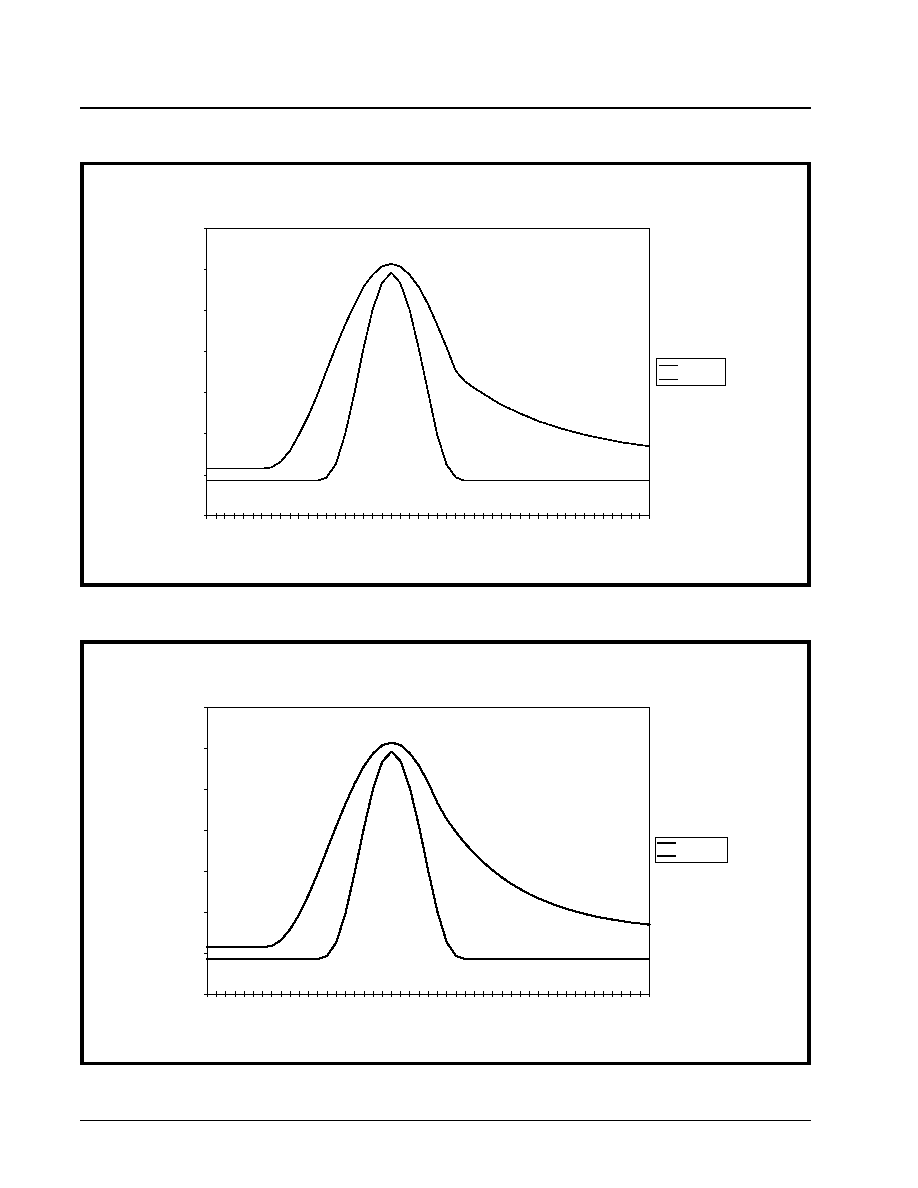
Figure 5 presents the test circuit that was used to test
and measure the pulse amplitudes as listed in the
ELECTRICAL CHARACTERISTICS tables.
Figure 6, Figure 7 and Figure 8 present the Pulse
Template requirements for the E3, DS3 and STS-1
Rates.
Receive Line Characteristics
Receive Sensitivity (Length of cable)
900
feet
Signal Level to Declare or Clear Loss of Signal (see Table 4)
mV
Intrinsic Jitter (all "1's" Pattern)
(2)
0.03
UI
Intrinsic Jitter (100 Pattern)
0.03
UI
Max Jitter Tolerance @ Jitter Frequency = 100Hz
64
UI
Max Jitter Tolerance @ Jitter Frequency = 1KHz
64
UI
Max Jitter Tolerance @ Jitter Frequency = 10KHz
5
UI
Max Jitter Tolerance @ Jitter Frequency = 800KHz
0.4
UI
AC ELECTRICAL CHARACTERISTICS (CONTINUED) (TA = 25
∞
C, VDD = 5.0V + 5%, UNLESS OTHER-
WISE SPECIFIED)
Line Side Parameters
S
YMBOL
P
ARAMETER
M
IN
.
T
YP
.
M
AX
.
U
NITS
ABSOLUTE MAXIMUM RATINGS
P
OWER
S
UPPLY
-0.5
TO
+6.5V
S
TORAGE
T
EMPERATURE
-65
O
C
TO
150
O
C
I
NPUT
V
OLTAGE
AT
A
NY
P
IN
-0.5V
TO
VDD +0.5V
P
OWER
D
ISSIPATION
TQFP P
ACKAGE
1.2W
I
NPUT
C
URRENT
AT
A
NY
P
IN
+100
M
A
ESD R
ATING
(M
IL
-S
TD
-883, M-3015)
A
T
L
EAST
1500V

·Á
·Á
·Á
·Á
XRT7300
E3/DS3/STS-1 LINE INTERFACE UNIT
REV. 1.1.1
15
F
IGURE
5. T
RANSMIT
P
ULSE
A
MPLITUDE
T
EST
C
IRCUIT
FOR
DS3, E3
AND
STS-1 R
ATES
R1
36
R2
36
TTIP
TRING
1:1
R3
75
T1
F
IGURE
6. ITU-T G.703 T
RANSMIT
O
UTPUT
P
ULSE
T
EMPLATE
FOR
E3 A
PPLICATIONS
0%
50%
V = 100%
14.55ns
Nominal Pulse
12.1ns
(14.55 - 2.45)
17 ns
(14.55 + 2.45)
8.65 ns
10%
10%
20%
XRT7300
·Á
·Á
·Á
·Á
E3/DS3/STS-1 LINE INTERFACE UNIT
REV. 1.1.1
16
F
IGURE
7. B
ELLCORE
GR-499-CORE T
RANSMIT
O
UTPUT
P
ULSE
T
EMPLATE
FOR
DS3 A
PPLICATIONS
DS3 Pulse Template
-0.2
0
0.2
0.4
0.6
0.8
1
1.2
-1
-0.9
-0.8
-0.7
-0.6
-0.5
-0.4
-0.3
-0.2
-0.1
0
0.1
0.2
0.3
0.4
0.5
0.6
0.7
0.8
0.9
1
1.1
1.2
1.3
1.4
Time, in UI
Normalized Amplitude
Lower Curve
Upper Curve
F
IGURE
8. B
ELLCORE
GR-253-CORE T
RANSMIT
O
UTPUT
P
ULSE
T
EMPLATE
FOR
SONET STS-1 A
PPLICATIONS
STS-1 Pulse Template
-0.2
0
0.2
0.4
0.6
0.8
1
1.2
-1
-0.9
-0.8
-0.7
-0.6
-0.5
-0.4
-0.3
-0.2
-0.1
0
0.1
0.2
0.3
0.4
0.5
0.6
0.7
0.8
0.9
1
1.1
1.2
1.3
1.4
Time, in UI
Normalized Amplitude
Lower Curve
Upper Curve
·Á
·Á
·Á
·Á
XRT7300
E3/DS3/STS-1 LINE INTERFACE UNIT
REV. 1.1.1
17
MICROPROCESSOR SERIAL INTERFACE TIMING (SEE FIGURE 9)
S
YMBOL
P
ARAMETER
M
IN
.
T
YP
.
M
AX
.
U
NITS
t
21
CS Low to Rising Edge of SCLK Setup Time
50
ns
t
22
CS High to Rising Edge of SCLK Hold Time
20
ns
t
23
SDI to Rising Edge of SCLK Setup Time
50
ns
t
24
SDI to Rising Edge of SCLK Hold Time
50
ns
t
25
SCLK "Low" Time
240
ns
t
26
SCLK "High" Time
240
ns
t
27
SCLK Period
500
ns
t
28
CS Low to Rising Edge of SCLK Hold Time
50
ns
t
29
CS Inactive Time
250
ns
t
30
Falling Edge of SCLK to SDO Valid Time
200
ns
t
31
Falling Edge of SCLK to SDO Invalid Time
100
ns
t
32
Falling Edge of SCLK or Rising Edge of CS to High Z
100
ns
t
33
Rise/Fall time of SDO Output
40
ns
F
IGURE
9. T
IMING
D
IAGRAM
FOR
THE
M
ICROPROCESSOR
S
ERIAL
I
NTERFACE
SDI
R/W
A1
A0
CS
SCLK
CS
SCLK
SDI
SDO
D0
D1
D2
D7
t22
t21
t23
t24
t25
t26
t27
t28
t29
t30
t31
t32
t33
Hi-Z
Hi-Z

XRT7300
·Á
·Á
·Á
·Á
E3/DS3/STS-1 LINE INTERFACE UNIT
REV. 1.1.1
18
SYSTEM DESCRIPTION
A functional block diagram of the XRT7300 E3/DS3/
STS-1 Transceiver IC (see Figure 1) shows that the
device contains three distinct sections:
∑ The Transmit Section
∑ The Receive Section
∑ The Microprocessor Serial Interface
THE TRANSMIT SECTION
The Transmit Section accepts TTL/CMOS level sig-
nals from the Terminal Equipment in either a Single-
Rail or Dual-Rail format. The Transmit Section then
takes this data and does the following:
∑ Encodes the data into the B3ZS format if the DS3
or SONET STS-1 Modes have been selected or
into the HDB3 format if the E3 Mode has been
selected.
∑ Converts the CMOS level B3ZS or HDB3 encoded
data into pulses with shapes that are compliant with
the various industry standard pulse template
requirements.
∑ Drives these pulses onto the line via the TTIP and
TRING output pins across a 1:1 Transformer.
N
OTE
: The Transmit Section drives a "1" (or a Mark) on the
line by driving either a positive or negative polarity pulse
across the 1:1 Transformer within a given bit period. The
Transmit Section drives a "0" (or a Space) onto the line by
driving no pulse onto the line.
THE RECEIVE SECTION
The Receive Section receives a bipolar signal from
the line either via a 1:1 Transformer or a 0.01mF Ca-
pacitor. As the Receive Section receives this line sig-
nal it does the following:
∑ Adjusts the signal level through an AGC circuit.
∑ Optionally equalizes this signal for cable loss.
∑ Attempts to quantify a bit-interval within the line sig-
nal as either a "1", "-1" or a "0" by slicing this data.
This sliced data is used by the Clock Recovery PLL
to recover the timing element within the line signal.
∑ The sliced data is routed to the HDB3/B3ZS
Decoder, during which the original data content as
transmitted by the Remote Terminal Equipment is
restored to its original content.
∑ Outputs the recovered clock and data to the Local
Terminal Equipment in the form of CMOS level sig-
nals via the RPOS, RNEG, RCLK1 and RCLK2 out-
put pins.
THE MICROPROCESSOR SERIAL INTERFACE
The XRT7300 can be configured to operate in either
the Hardware Mode or the HOST Mode.
The Hardware Mode
Connect the HOST/HW input pin (pin 18) to GND to
configure the XRT7300 to operate in the Hardware
Mode.
When the XRT7300 is operating in the Hardware
Mode, the following is true:
1. The Microprocessor Serial Interface block is
disabled.
2. The XRT7300 is configured via input pin settings.
Each of the pins associated with the Microprocessor
Serial Interface takes on their alternative role as de-
fined in Table 1.
3. All of the remaining input pins become active.
T
ABLE
1: R
OLE
OF
M
ICROPROCESSOR
S
ERIAL
I
NTERFACE
PINS
WHEN
THE
XRT7300
IS
OPERATING
IN
THE
H
ARDWARE
M
ODE
P
IN
#
P
IN
N
AME
F
UNCTION
WHILE
IN
THE
H
ARDWARE
M
ODE
11
REGRESET/(RCLK2INV)
RCLK2INV
19
SDI/(LOSMUTEN)
LOSMUTEN
20
SDO/(LCV)
LCV
21
SCLK/(ENCODIS)
ENCODIS
22
CS/(DECODIS)
DECODIS
30
LCV/(RCLK2)
RCLK2
·Á
·Á
·Á
·Á
XRT7300
E3/DS3/STS-1 LINE INTERFACE UNIT
REV. 1.1.1
19
The HOST Mode
To configure the XRT7300 to operate in the HOST
Mode, connect the HOST/HW input pin (pin 18) to
VDD.
When the XRT7300 is operating in the HOST Mode,
the following is true:
1. The Microprocessor Serial Interface block is
enabled. Many configuration selections are
made by writing the appropriate data into the on-
chip Command Registers via the Microprocessor
Serial Interface.
2. All of the following input pins are disabled:
∑ Pin 1 - TXLEV
∑ Pin 2 - TAOS
∑ Pin 12 - REQDIS
∑ Pin 14 - LLB
∑ Pin 15 - RLB
∑ Pin 16 - STS-1/DS3
∑ Pin 17 - E3
∑ Pin 35 - TXOFF
Tie each of these pins to GND if the XRT7300 IC is to
be operated in the HOST Mode.
Please see Section 5.0 for a detailed description on
operating the Microprocessor Serial Interface or the
on-chip Command Registers.
1.0
SELECTING THE DATA RATE
The XRT7300 can be configured to support the E3
(34.368 Mbps), DS3 (44.736 Mbps) or the SONET
STS-1 (51.84 Mbps) rates. Selection of the data rate
is dependent on whether the XRT7300 is operating in
the Hardware or HOST Mode.
A. When operating in the Hardware Mode.
To configure the XRT7300 for the desired data rate,
the E3 and the STS-1/DS3 pins must be set to the ap-
propriate logic states shown in Table 2.
B. When operating in the HOST Mode.
To configure the XRT7300 for the desired data rate,
appropriate values need to be written into the STS-1/
DS3 and E3 bit-fields in Command Register CR4.
Table 3 relates the values of these two bit-fields with
respect to the selected data rates.
The results of making these selections are:
1. The VCO Center Frequency of the Clock Recov-
ery Phase-Locked-Loop is configured to match
the selected data rate.
2. The B3ZS/HDB3 Encoder and Decoder blocks
are configured to support B3ZS Encoding/Decod-
ing if the DS3 or STS-1 data rates were selected
or,
3. The B3ZS/HDB3 Encoder and Decoder blocks
are configured to support HDB3 Encoding/
Decoding if the E3 data rate was selected.
4. The on-chip Pulse-Shaping circuitry is configured
to generate Transmit Output pulses of the correct
T
ABLE
2: S
ELECTING
THE
D
ATA
R
ATE
FOR
THE
XRT7300
VIA
THE
E3
AND
STS-1/DS3
INPUT
PINS
(H
ARDWARE
M
ODE
)
D
ATA
R
ATE
S
TATE
OF
E3 P
IN
(P
IN
17)
S
TATE
OF
STS-1/DS3
PIN
(P
IN
16)
M
ODE
OF
B3ZS/HDB3 E
NCODER
/
D
ECODER
B
LOCKS
E3 (34.368 Mbps)
VDD
X (Don't Care)
HDB3
DS3 (44.736 Mbps)
0
0
B3ZS
STS-1 (51.84 Mbps)
0
VDD
B3ZS
COMMAND REGISTER CR4 (ADDRESS = 0X04)
D4
D3
D2
D1
D0
X
STS-1/DS3
E3
LLB
RLB
X
X
X
X
X
T
ABLE
3: S
ELECTING
THE
D
ATA
R
ATE
FOR
THE
XRT7300 V
IA
THE
STS-1/DS3
AND
THE
E3 B
IT
-
FIELDS
W
ITHIN
C
OMMAND
R
EGISTER
CR4 (HOST M
ODE
)
S
ELECTED
D
ATA
R
ATE
STS-1/DS3
E3
E3
Don't Care
1
DS3
0
0
STS-1
1
0
XRT7300
·Á
·Á
·Á
·Á
E3/DS3/STS-1 LINE INTERFACE UNIT
REV. 1.1.1
20
shape and width to meet the applicable pulse
template requirement.
5. The LOS Declaration/Clearance Criteria is estab-
lished.
2.0
THE TRANSMIT SECTION
Figure 1 indicates that the Transmit Section of the
XRT7300 consists of the following blocks:
∑ Transmit Logic Block
∑ Duty Cycle Adjust Block
∑ HDB3/B3ZS Encoder
∑ Pulse Shaping Block
The purpose of the Transmit Section in the XRT7300
is to take TTL/CMOS level data from the terminal
equipment and encode it into a format that can:
1. be efficiently transmitted over coaxial cable at E3,
DS3 or STS-1 data rates.
2. be reliably received by the Remote Terminal at
the other end of the E3, DS3 or STS-1 data link.
3. comply with the applicable pulse template
requirements.
2.1
T
HE
T
RANSMIT
L
OGIC
B
LOCK
The purpose of the Transmit Logic Block is to accept
either Dual-Rail or Single-Rail (a binary data stream)
TTL/CMOS level data and timing information from the
Terminal Equipment.
Accepting Dual-Rail Data from the Terminal
Equipment
The XRT7300 accepts Dual-Rail data from the Termi-
nal Equipment via the following input signals:
∑ TPDATA
∑ TNDATA
∑ TCLK
Figure 10 illustrates the typical interface for the trans-
mission of data in a Dual-Rail Format between the
Terminal Equipment and the Transmit Section of the
XRT7300.
F
IGURE
10. T
HE
T
YPICAL
I
NTERFACE
FOR
THE
T
RANSMISSION
OF
D
ATA
IN
A
D
UAL
-R
AIL
F
ORMAT
F
ROM
THE
T
RANS
-
MITTING
T
ERMINAL
E
QUIPMENT
TO
THE
T
RANSMIT
S
ECTION
OF
THE
XRT7300
Exar E3/DS3/STS-1 LIU
Terminal
Equipment
(E3/DS3 or STS-1
Framer)
Terminal
Equipment
(E3/DS3 or STS-1
Framer)
TxPOS
TxNEG
TxLineClk
Transmit
Logic
Block
Transmit
Logic
Block
TPDATA
TNDATA
TCLK
F
IGURE
11. H
OW
THE
XRT7300 S
AMPLES
THE
D
ATA
ON
THE
TPDATA
AND
TNDATA I
NPUT
P
INS
TCLK
TPDATA
TNDATA
Data 1 1 0 0

·Á
·Á
·Á
·Á
XRT7300
E3/DS3/STS-1 LINE INTERFACE UNIT
REV. 1.1.1
21
The manner that the LIU handles Dual-Rail data is
described below and illustrated in Figure 11. The
XRT7300 typically samples the data on the TPDATA
and TNDATA input pins on the falling edge of TCLK.
TCLK is typically a clock signal that is of the selected
data rate frequency. For the E3 data rate, TCLK is
34.368 MHz. For the DS3 data rate, TCLK is 44.736
MHz and for the SONET STS-1 rate, TCLK is 51.84
MHz. In general, if the XRT7300 samples a "1" on
the TPDATA input pin, the Transmit Section of the de-
vice ultimately generates a positive polarity pulse via
the TTIP and TRING output pins across a 1:1 trans-
former. If the XRT7300 samples a "1" on the TNDATA
input pin, the Transmit Section of the device ultimately
generates a negative polarity pulse via the TTIP and
TRING output pins across a 1:1 transformer.
2.1.1
Accepting Single-Rail Data from the Ter-
minal Equipment
Do the following if data is to be transmited from the
Terminal Equipment to the XRT7300 in Single-Rail
format (a binary data stream) without having to con-
vert it into a Dual-Rail format.
A. Configure the XRT7300 to operate in the HOST
Mode or,
B. access the Microprocessor Serial Interface and
write a "1" into the TXBIN (TRANSMIT BINary)
bit-field in Command Register 1.
After taking these steps, the Transmit Logic Block ac-
cepts Single-Rail data via the TPDATA input pin. The
XRT7300 samples this input pin on the falling edge of
the TCLK clock signal and encodes it into the appro-
priate bipolar line signal across the TTIP and TRING
output pins.
N
OTES
:
1. In this mode the Transmit Logic Block ignores the
TNDATA input pin.
2. If the Transmit Section of the XRT7300 is config-
ured to accept Single-Rail data from the Terminal
Equipment, the B3ZS/HDB3 Encoder must be
enabled.
Figure 12 illustrates the behavior of the TPDATA and
TCLK signals when the Transmit Logic Block has
been configured to accept Single-Rail data from the
Terminal Equipment.
2.2
T
HE
T
RANSMIT
C
LOCK
D
UTY
C
YCLE
A
DJUST
C
IR
-
CUITRY
The on-chip Pulse-Shaping circuitry (in the Transmit
Section of the XRT7300) has the responsibility for
generating pulses of the shape and width to comply
with the applicable pulse template requirement. The
widths of these output pulses are defined by the width
of the half-period pulses in the TCLK signal.
Allowing the widths of the pulses in the TCLK clock
signal to vary significantly could jeopardize the chip's
ability to generate Transmit Output pulses of the ap-
propriate width, thereby failing the applicable Pulse
Template Requirement Specification. Consequently,
the chips ability to generate compliant pulses could
depend upon the duty cycle of the clock signal ap-
plied to the TCLK input pin.
In order to combat this phenomenon, the Transmit
Clock Duty Cycle Adjust circuit was designed into the
XRT7300. The Transmit Clock Duty Cycle Adjust Cir-
cuitry is a PLL that was designed to accept clock
pulses via the TCLK input pin at duty cycles ranging
from 30% to 70% and to regenerate these signals
with a 50% duty cycle.
COMMAND REGISTER CR1 (ADDRESS = 0X01)
D4
D3
D2
D1
D0
TXOFF
TAOS
TXCLKINV
TXLEV
TXBIN
X
X
X
X
1
F
IGURE
12. T
HE
B
EHAVIOR
OF
THE
TPDATA
AND
TCLK I
NPUT
S
IGNALS
W
HILE
THE
T
RANSMIT
L
OGIC
B
LOCK
IS
A
CCEPTING
S
INGLE
-R
AIL
D
ATA
F
ROM
THE
T
ERMINAL
E
QUIPMENT
TCLK
TPDATA
Data 1 1 0 0
XRT7300
·Á
·Á
·Á
·Á
E3/DS3/STS-1 LINE INTERFACE UNIT
REV. 1.1.1
22
The XRT7300 Transmit Clock Duty Cycle Adjust cir-
cuit alleviates the need to supply a signal with a 50%
duty cycle to the TCLK input pin.
2.3
T
HE
HDB3/B3ZS E
NCODER
B
LOCK
The purpose of the HDB3/B3ZS Encoder Block is to
aid in the Clock Recovery process (at the Remote
Terminal Equipment) by ensuring an upper limit on
the number of consecutive zeros that can exist in the
line signal.
2.3.1
B3ZS Encoding
If the XRT7300 is configured to operate in the DS3 or
SONET STS-1 Modes, then the HDB3/B3ZS Encoder
block operates in the B3ZS Mode. When the Encoder
is operating in this mode, it parses through and
searches the Transmit Binary Data Stream (from the
Transmit Logic Block) for the occurrence of three (3)
consecutive zeros ("000"). If the B3ZS Encoder finds
an occurrence of three consecutive zeros, it substi-
tutes these three "0's" with either a "00V" or a "B0V"
pattern.
"B" represents a Bipolar pulse that is compliant with
the Alternating Polarity requirements of the AMI (Al-
ternate Mark Inversion) line code and "V" represents
a bipolar Violation (e.g., a bipolar pulse that violates
the Alternating Polarity requirements of the AMI line
code).
The B3ZS Encoder decides whether to substitute
with either a "00V" or a "B0V" pattern in order to in-
sure that an odd number of bipolar pulses exist be-
tween any two consecutive violation pulses.
Figure 13 illustrates the B3ZS Encoder at work with
two separate strings of three (or more) consecutive
zeros.
2.3.2
HDB3 Encoding
If the XRT7300 is configured to operate in the E3
Mode, then the HDB3/B3ZS Encoder block operates
in the HDB3 Mode. When the Encoder is operating in
this mode, it parses through and searches the Trans-
mit Data Stream (from the Transmit Logic Block) for
the occurrence of four (4) consecutive zeros ("0000").
If the HDB3 Encoder finds an occurrence of four con-
secutive zeros, then it substitutes these four "0's" with
either a "000V" or a "B00V" pattern in order to insure
that an odd number of bipolar pulses exist between
any two consecutive violation pulses.
F
IGURE
13. A
N
E
XAMPLE
OF
B3ZS E
NCODING
Data
TPDATA
TNDATA
1 0 1 1 0 0 0 1 0 1 1 1 1 0 1 1 0 1 1 0 0 1 1 1 0 0 0 1
0 0 V
Line Signal
B 0 V
TCLK
·Á
·Á
·Á
·Á
XRT7300
E3/DS3/STS-1 LINE INTERFACE UNIT
REV. 1.1.1
23
Figure 14 illustrates the HDB3 Encoder at work with
two separate strings of four (or more) consecutive ze-
ros.
2.3.3
Enabling/Disabling the HDB3/B3ZS
Encoder
The XRT7300 allows two methods to enable or dis-
able the HDB3/B3ZS Encoder.
If the XRT7300 is operating in the Hardware Mode.
To enable the HDB3/B3ZS Encoder, set the ENCO-
DIS input pin (pin 21) to "0". To disable the HDB3/
B3ZS Encoder, set the ENCODIS input pin (pin 21) to
"1".
If the XRT7300 is operating in the HOST Mode.
To enable the HDB3/B3ZS Encoder, set the ENCO-
DIS bit-field in Command Register (CR2) to "0".
To disable the HDB3/B3ZS Encoder, set the ENCO-
DIS bit-field in Command Register (CR2) to "1".
If either of these two methods is employed to disable
the HDB3/B3ZS Encoder, the LIU transmits the data
onto the line as it is received via the TPDATA and
TNDATA input pins.
2.4
T
HE
T
RANSMIT
P
ULSE
S
HAPER
C
IRCUITRY
The Transmit Pulse Shaper Circuitry consists of a
Transmit Line Build-Out circuit which can be enabled
or disabled by setting the TXLEV input pin (or TXLEV
bit-field) to "High" or "Low". The purpose of the
Transmit Line Build-Out circuit is to permit configuring
of the XRT7300 to transmit an output pulse which is
compliant to either of the following Bellcore pulse
template requirements when measured at the Digital
Cross Connect System. Each of these Bellcore spec-
ifications further state that the cable length between
the Transmit Output and the Digital Cross Connect
system can range anywhere from 0 to 450 feet.
The Isolated DSX-3 Pulse Template Requirement per
Bellcore GR-499-CORE is illustrated in Figure 7.
The Isolated STSX-1 Pulse Template Requirement
per Bellcore GR-253-CORE is illustrated in Figure 8.
2.4.1
Enabling the Transmit Line Build-Out Cir-
cuit
If the Transmit Line Build-Out Circuit is enabled, the
XRT7300 outputs shaped pulses onto the line via the
TTIP and TRING output pins.
Do the following to enable the Transmit Line Build-Out
circuit in the XRT7300:
∑ If the XRT7300 is operating in the Hardware Mode,
set theTXLEV input pin (pin 1) to "Low"
∑ If the XRT7300 is operating in the HOST Mode, set
the TXLEV bit-field to "0" as illustrated below.
2.4.2
Disabling the Transmit Line Build-Out Cir-
cuit
F
IGURE
14. A
N
E
XAMPLE
OF
HDB3 E
NCODING
Data
TPDATA
TNDATA
1 0 1 1 0 0 0 0 0 1 1 1 1 0 1 1 0 1 1 0 0 1 1 0 0 0 0 1
0 0 0 V
Line Signal
B 0 0 V
TCLK
COMMAND REGISTER CR2 (ADDRESS = 0X02
D4
D3
D2
D1
D0
DECODIS ENCODIS ALOSDIS DLOSDIS
REQDIS
X
0
X
X
X
COMMAND REGISTER CR1 (ADDRESS = 0X01)
D4
D3
D2
D1
D0
TXOFF
TAOS
TXCLKINV
TXLEV
TXBIN
0
X
X
0
1

XRT7300
·Á
·Á
·Á
·Á
E3/DS3/STS-1 LINE INTERFACE UNIT
REV. 1.1.1
24
If the Transmit Line Build-Out circuit is disabled, then
the XRT7300 outputs partially-shaped pulses onto
the line via the TTIP and TRING output pins.
Disable the Transmit Line Build-Out circuit in the
XRT7300 by doing the following:
∑ If the XRT7300 is operating in the Hardware Mode,
set the TXLEV input pin (pin 1) to "High"
∑ If the XRT7300 is operating in the HOST Mode, set
the TXLEV bit-field to "1" as illustrated below.
2.4.3
Design Guideline for Setting the Transmit
Line Build-Out Circuit
The setting ofTXLEV input pin or bit-field should be
based upon the overall cable length between the
Transmitting Terminal and the Digital Cross Connect
system (where the pulse template measurements are
made).
If the cable length between the Transmitting Terminal
and the DSX-3 or STSX-1 is less than 225 feet, it is
advisable to enable the Transmit Line Build-Out circuit
by setting the TXLEV input pin or bit-field to "0".
N
OTE
: In this case the XRT7300 outputs shaped (e.g., not
square-wave) pulses onto the line via the TTIP and TRING
output pins. The shape of this output pulse is such that it
complies with the pulse template requirements even when
subjected to cable loss ranging from 0 to 225 feet.
If the cable length between the Transmitting
Terminal and the DSX-3 or STSX-1 is greater than
225 feet, it is advisable to disable the Transmit Line
Build-Out circuit by setting the TXLEV input pin or bit-
field to "1".
N
OTE
: In this case the XRT7300 outputs partially-shaped
pulses onto the line via the TTIP and TRING output pins.
The cable loss that these pulses experience over long cable
lengths (e.g., greater than 225 feet) causes these pulses to
be properly shaped and comply with the appropriate pulse
template requirement.
2.4.4
The Transmit Line Build-Out Circuit and
E3 Applications
The ITU-T G.703 Pulse Template Requirements for
E3 states that the E3 transmit output pulse should be
measured at the Secondary Side of the Transmit Out-
put Transformer for Pulse Template compliance. In
other words, there is no Digital Cross Connect Sys-
tem pulse template requirement for E3 and the Trans-
mit Line Build-Out circuit in the XRT7300 is disabled
whenever it is operating in the E3 Mode.
2.5
I
NTERFACING
THE
T
RANSMIT
S
ECTION
OF
THE
XRT7300
TO
THE
L
INE
The E3, DS3 and SONET STS-1 specification docu-
ments all state that line signals transmitted over coax-
ial cable are to be terminated with 75 Ohms. There-
fore, interface the Transmit Section of the XRT7300,
as illustrated in Figure 15 which shows two 36 Ohm
resistors in series with the primary side of the trans-
former. These two 36Ohm resistors closely match
the 75Ohm load termination resistor thereby minimiz-
ing Transmit Return Loss.
COMMAND REGISTER CR1 (ADDRESS = 0X01)
D4
D3
D2
D1
D0
TXOFF
TAOS
TXCLKINV
TXLEV
TXBIN
0
X
X
1
1
F
IGURE
15. R
ECOMMENDED
S
CHEMATIC
FOR
I
NTERFACING
THE
T
RANSMIT
S
ECTION
OF
THE
XRT7300
TO
THE
L
INE
R1
36.0
R2
36.0
TTIP
TRING
1:1
BNC
T1

·Á
·Á
·Á
·Á
XRT7300
E3/DS3/STS-1 LINE INTERFACE UNIT
REV. 1.1.1
25
TRANSFORMER VENDOR INFORMATION
Pulse
Corporate Office
12220 World Trade Drive
San Diego, CA 92128
Tel: (619)-674-8100
FAX: (619)-674-8262
Europe
1 & 2 Huxley Road
The Surrey Research Park
Guildford, Surrey GU2 5RE
United Kingdom
Tel: 44-1483-401700
FAX: 44-1483-401701
Asia
150 Kampong Ampat
#07-01/02
KA Centre
Singapore 368324
Tel: 65-287-8998
FAX: 65-280-0080
3.0
THE RECEIVE SECTION
Figure 1 indicates that the XRT7300 Receive Section
consists of the following blocks:
∑ AGC/Equalizer
∑ Peak Detector
∑ Slicer
∑ Clock Recovery PLL
∑ Data Recovery
∑ HDB3/B3ZS Decoder
The purpose of the XRT7300 Receive Section is to
take an incoming attenuated/distorted bipolar signal
from the line and encode it back into the TTL/CMOS
format where it can be received and processed by
digital circuitry in the Terminal Equipment.
3.1
I
NTERFACING
THE
R
ECEIVE
S
ECTION
OF
THE
XRT7300
TO
THE
L
INE
By design, the Receive Section of the XRT7300 can
be transformer-coupled or capacitive-coupled to the
line. The specification documents for E3, DS3 and
STS-1 all specify 75Ohm termination loads when
transmitting over coaxial cable. It is recommended to
TRANSFORMER RECOMMENDATIONS
P
ARAMETER
V
ALUE
Turns Ratio
1:1
Primary Inductance
40
µ
H
Isolation Voltage
1500Vrms
Leakage Inductance
0.6
µ
H
P
ART
N
UMBER
V
ENDOR
I
NSULATION
P
ACKAGE
T
YPE
PE-68629
Pulse
3000V
Large Thru-Hole
PE-65966
Pulse
1500V
Small Thru-Hole
PE-65967
Pulse
1500V
Small SMT
T3001
Pulse
1500V
Small SMT
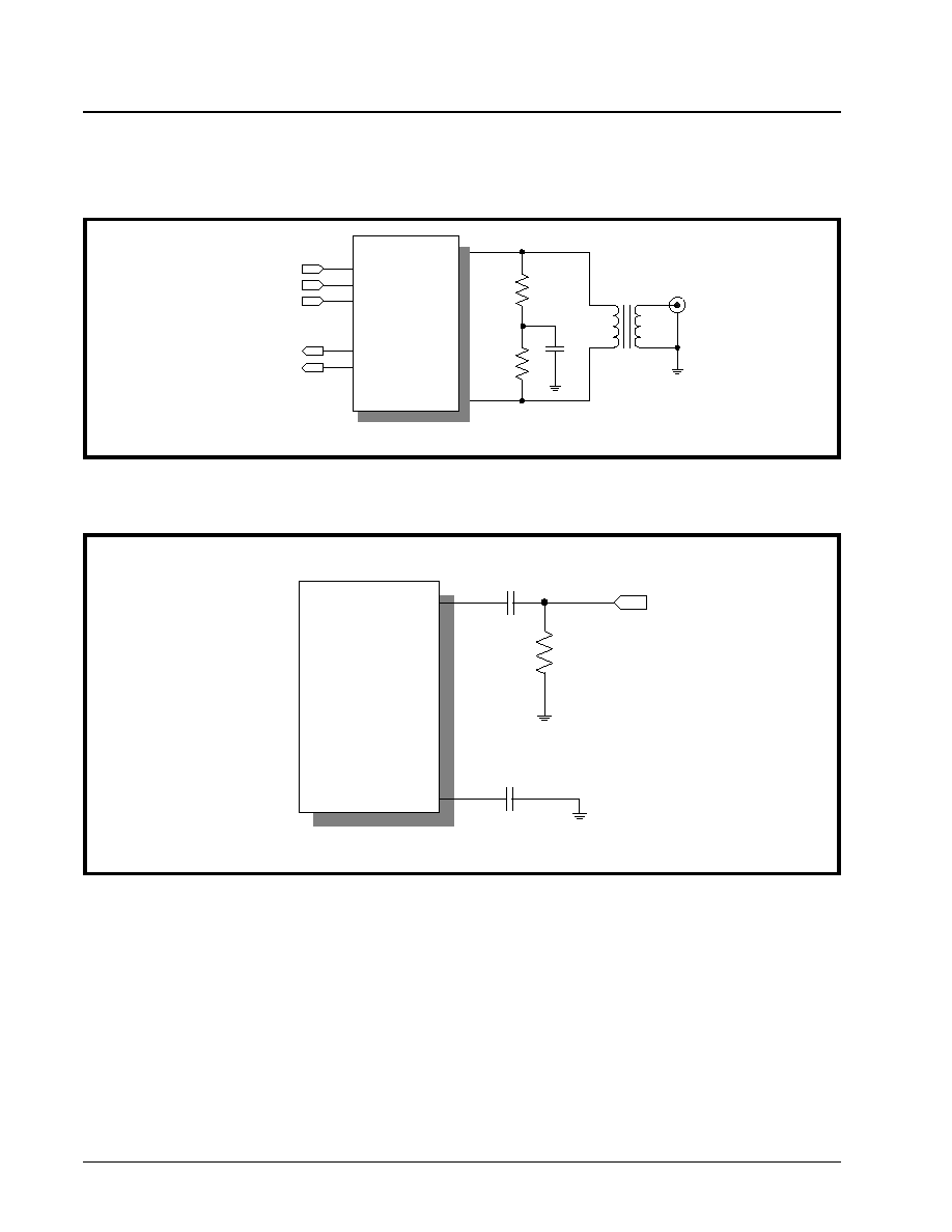
XRT7300
·Á
·Á
·Á
·Á
E3/DS3/STS-1 LINE INTERFACE UNIT
REV. 1.1.1
26
interface the Receive Section of the XRT7300 to the
line as shown in Figure 16 or Figure 17.
3.2
T
HE
R
ECEIVE
E
QUALIZER
B
LOCK
After the XRT7300 has received the incoming line
signal via the RTIP and RRING input pins, the first
block that this signal passes through is the AGC cir-
cuit followed by the Receive Equalizer.
As the line signal is transmitted from a given transmit-
ting terminal, the pulse shapes at that location are ba-
sically square. Hence, these pulses consist of a com-
bination of "Low" and "High" frequency Fourier com-
ponents. As this line signal travels from the transmit-
ting terminal via the coaxial cable to the receiving
terminal, it is subjected to frequency-dependent loss.
In other words, the higher-frequency components of
the signal is subjected to a greater amount of attenu-
ation than the lower-frequency components. If this
line signal travels over reasonably long cable lengths
(e.g., greater than 450 feet), then the shape of the
pulses (which were originally square) is distorted and
inter-symbol interference increases.
The purpose of the Receive Equalizer is to equalize
the distortion of the incoming signal due to cable loss.
The Receive Equalizer accomplishes this by subject-
ing the received line signal to frequency-dependent
amplification (which attempts to counter the frequen-
cy dependent loss that the line signal has experi-
enced) and to restore the shape of the line signal so
F
IGURE
16. R
ECOMMENDED
S
CHEMATIC
FOR
I
NTERFACING
THE
R
ECEIVE
S
ECTION
OF
THE
XRT7300
TO
THE
L
INE
(T
RANSFORMER
-C
OUPLING
)
BNC
1:1
R1
37.5
R2
37.5
RTIP
RRING
C1
0.01uF
RPOS
RNEG
RCLK1
RLOS
RLOL
RxLOS
RxLOL
RxPOS
RxNEG
RxLineClk
T2
F
IGURE
17. R
ECOMMENDED
S
CHEMATIC
FOR
I
NTERFACING
THE
R
ECEIVE
S
ECTION
OF
THE
XRT7300
TO
THE
L
INE
(C
APACITIVE
-C
OUPLING
)
R1
75
RTIP
RRING
C1
0.01uF
C2
0.01uF
Receive Line Signal
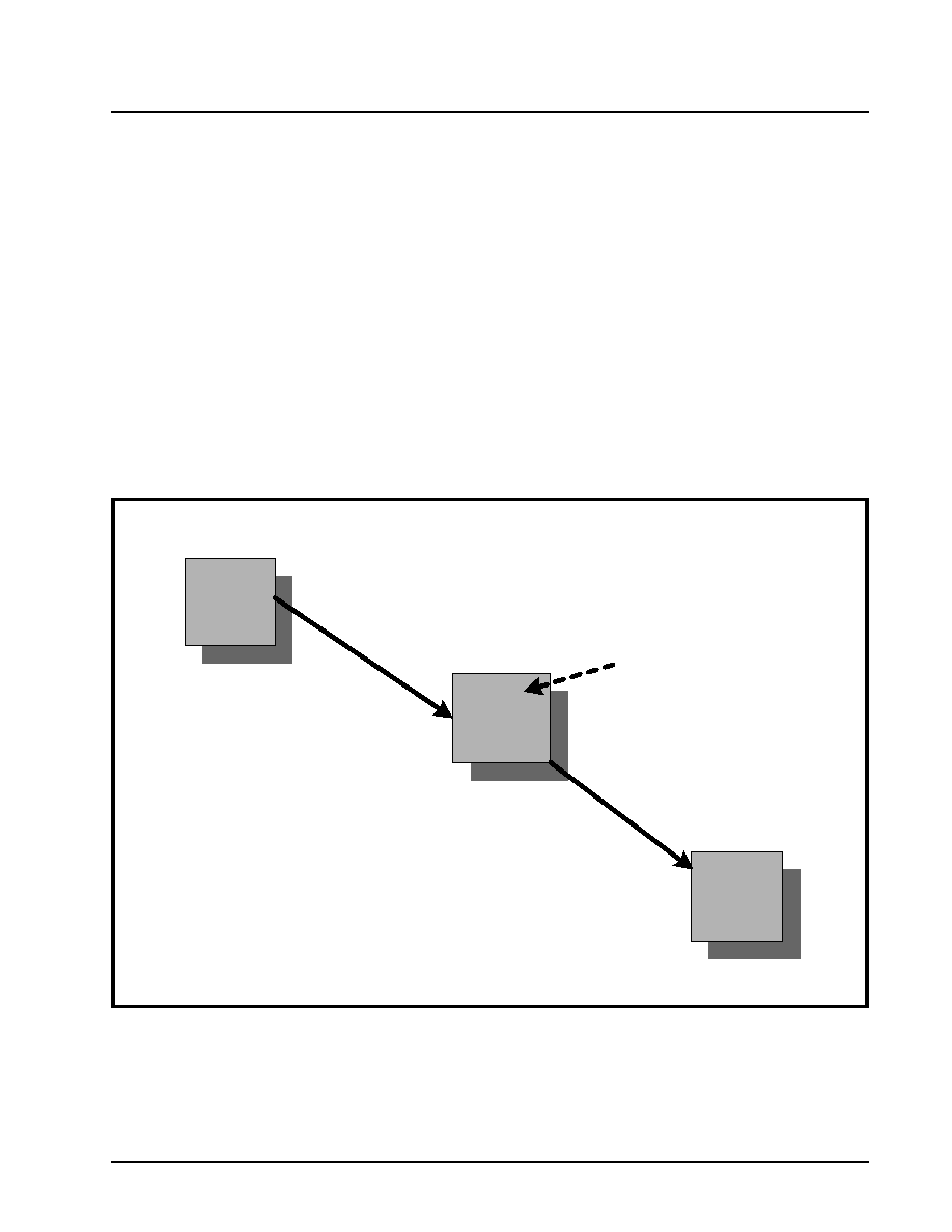
·Á
·Á
·Á
·Á
XRT7300
E3/DS3/STS-1 LINE INTERFACE UNIT
REV. 1.1.1
27
that the transmitted data and clock can be recovered
reliably.
The Use of the Receive Equalizer in a Typical DS3
or STS-1 Application
Most System Manufacturers of equipment supporting
DS3 and STS-1 lines interface their equipment to a
Digital Cross-Connect System. While installing their
equipment, the Transmit Line Build-Out circuit is set
to the proper setting that makes the transmit output
pulse compliant with the Isolated DSX-3 or STSX-1
Pulse Template requirements. For the XRT7300 this
is achieved by setting the TXLEV input pin or bit-field
to the appropriate level.
When the System Manufacturer is interfacing the Re-
ceive Section of the XRT7300 to the Digital Cross-
Connect system, they should keep aware of the fol-
lowing facts:
1. By definition, all DS3 or STS-1 line signals that
are present at the Digital Cross-Connect system
are required to meet the Isolated Pulse Template
Requirements per Bellcore GR-499-CORE for
DS3 applications or Bellcore GR-253-CORE for
STS-1 applications.
2. Further, these Bellcore documents state that the
amplitude of these pulses at the DSX-3 or STSX-
1 can range in amplitude from 360mVpk to
850mVpk.
3. Finally, these Bellcore documents stipulate that
the Receiving Terminal must be able to receive
this pulse-template compliant line signal over a
cable length of 0 to 450 feet from the Digital
Cross Connect system.
These facts are reflected in Figure 18.
Design Considerations for DS3 and STS-1 Appli-
cations
When installing equipment into environments as de-
picted in Figure 15, it is recommended that the Re-
ceive Equalizer be enabled by setting the REQDIS in-
put pin or bit-field to "0". In fact, the only time that the
Receive Equalizer should be disabled is when there
is an off-chip equalizer in the Receive path between
the Digital Cross-Connect system and the RTIP/
RRING input pins or, in applications where the Re-
ceiver is monitoring the transmit output signal directly.
F
IGURE
18. T
HE
T
YPICAL
A
PPLICATION
FOR
THE
S
YSTEM
I
NSTALLER
DSX-3
or
STSX-1
Digital Cross-
Connect System
Transmitting
Terminal
Receiving
Terminal
0 to 450 feet of
C a b l e
Pulses that are
compliant to the
Isolated DSX-3 or
STSX-1 Pulse
Template
Requirement
0 to 450 feet of
C a b l e

XRT7300
·Á
·Á
·Á
·Á
E3/DS3/STS-1 LINE INTERFACE UNIT
REV. 1.1.1
28
Design Considerations for E3 Applications or if
the Overall Cable Length is known
Figure 18 indicates the following:
A. the length of cable between the Transmitting Ter-
minal and the Digital Cross-Connect system can
range between 0 and 450 feet and
B. the length of cable between the Digital Cross-
Connect system and the Receive Terminal can
range between 0 and 450 feet.
The overall cable length between the Transmitting
Terminal and the Receiving Terminal can range be-
tween very short cable length (near 0 feet) up to 900
feet.
If during system installation the overall cable length is
known, then (to optimize the performance of the
XRT7300 in terms of receive jitter performance, etc.),
the Receive Equalizer should be enabled or disabled
based upon the following recommendations:
The Receive Equalizer should be turned ON if the
Receive Section is going to receive a line signal with
an overall cable length of 300 feet or greater. The
Receive Equalizer should be turned OFF if the Re-
ceive Section is going to receive a line signal over a
cable length of less than 300 feet.
N
OTES
:
1. If the Receive Equalizer block is turned ON (in a
given Receive Section that is receiving a line signal
over short cable length), there is the risk of over-
equalizing the received line signal which could
degrade performance by increasing the amount of
jitter that exists in the recovered data and clock sig-
nals or by creating bit-errors.
2. The Receive Equalizer has been designed to
counter the frequency-dependent cable loss that a
line signal experiences as it travels from the Trans-
mitting Terminal to the Receiving Terminal. How-
ever, Receive Equalizer was not designed to
counter flat loss where all of the Fourier frequency
components in the line signal are subject to the
same amount of attenuation. Flat loss is handled
by the AGC block.
The Receive Equalizer block can be disabled setting
the REQDIS input pin "High" when operating in the
Hardware Mode or writing a "1" to the REQDIS bit-
field in Command Register CR2 when operating the
XRT7300 in the HOST Mode.
3.3
P
EAK
D
ETECTOR
AND
S
LICER
After the incoming line signal has passed through the
Receive Equalizer it is routed to the Slicer block. The
purpose of the Slicer is to quantify a given bit-period
(or symbol) within the incoming line signal as either a
"1" or a "0".
3.4
C
LOCK
R
ECOVERY
PLL
The output of the Slicer, which is now Dual-Rail digital
pulses, is routed to the Clock Recovery PLL. The
purpose of the Clock Recovery PLL is to track the in-
coming Dual-Rail data stream and to derive and gen-
erate a recovered clock signal.
It is important to note that the Clock Recovery PLL re-
quires a line rate clock signal at the EXCLK input pin.
The Clock Recovery PLL operates in one of two
modes:
∑ The Training Mode.
∑ The Data/Clock Recovery Mode
1. The Training Mode
If the XRT7300 is not receiving a line signal via the
RTIP and RRING input pins or if the frequency differ-
ence between the line signal and that applied via the
EXCLK input pin exceeds 0.5%, then the XRT7300
LIU IC is operating in the Training Mode. When the
LIU is operating in the Training Mode it does the fol-
lowing:
A. declares a Loss of Lock indication by toggling the
RLOL output pin "High" and
B. outputs a clock signal via the RCLK1 and RCLK2
output pins which is derived from the signal ap-
plied to the EXCLK input pin.
2. The Data/Clock Recovery Mode
If the frequency difference between the line signal
and that applied via the EXCLK input pin is less than
0.5%, the XRT7300 LIU IC is operating in the Data/
Clock Recovery Mode. In this mode, the Clock Re-
covery PLL is locked onto the line signal via the RTIP
and RRING input pins.
3.5
T
HE
HDB3/B3ZS D
ECODER
The Remote Transmitting Terminal typically encodes
the line signal into some sort of Zero Suppression
Line Code (e.g., HDB3 for E3 and B3ZS for DS3 and
STS-1). The purpose of this encoding activity was to
aid in the Clock Recovery process of this data in the
Near-End Receiving Terminal. However, once the da-
ta has made it across the E3, DS3 or STS-1 Trans-
port Medium and has been recovered by the Clock
Recovery PLL, it is now necessary to restore the orig-
inal content of the data. The purpose of the HDB3/
B3ZS Decoding block is to restore the data (transmit-
COMMAND REGISTER CR2 (ADDRESS = 0X02)
D4
D3
D2
D1
D0
DECODIS ENCODIS ALOSDIS DLOSDIS
REQDIS
X
0
X
X
1

·Á
·Á
·Á
·Á
XRT7300
E3/DS3/STS-1 LINE INTERFACE UNIT
REV. 1.1.1
29
ted over the E3, DS3 or STS-1 line) to its original con-
tent prior to Zero Suppression encoding.
3.5.1
B3ZS Decoding DS3/STS-1 Applications
If the XRT7300 is configured to operate in the DS3 or
STS-1 Modes, then the HDB3/B3ZS Decoding Block
performs B3ZS Decoding. When the Decoder is op-
erating in this mode it parses through the incoming
Dual-Rail data and checks for the occurrence of ei-
ther a "00V" or a "B0V" pattern. If the B3ZS Decoder
detects this particular pattern it substitutes these bits
with a "000" pattern.
N
OTE
: If the B3ZS Decoder detects any bipolar violations
that is not in accordance with the"B3ZS Line Code" format,
or if the B3ZS Decoder detects a string of 3 (or more) con-
secutive "0's" in the incoming line signal, then the B3ZS
Decoder flags this event as a Line Code Violation by puls-
ing the LCV output pin "High".
Figure 19 illustrates the B3ZS Decoder at work with
two separate Zero Suppression patterns in the in-
coming Dual-Rail Data Stream.
3.5.2
HDB3 Decoding E3 Applications
If the XRT7300 is configured to operate in the E3
Mode, the HDB3/B3ZS Decoding Block performs
HDB3 Decoding. When the Decoder is operating in
this mode it parses through the incoming Dual-Rail
data and checks for the occurrence of either a "000V"
or a "B00V" pattern. If the HDB3 Decoder detects
this particular pattern, it substitutes these bits with a
"0000" pattern.
Figure 20 illustrates the HDB3 Decoder at work with
two separate Zero Suppression patterns in the in-
coming Dual-Rail Data Stream.
N
OTE
: If the HDB3 Decoder detects any bipolar violation
(e.g., "V") pulses that is not in accordance with the HDB3
Line Code format, or if the HDB3 Decoder detects a string
of 4 (or more) "0's" in the incoming line signal, then the
HDB3 Decoder flags this event as a Line Code Violation by
pulsing the LCV output pin "High".
F
IGURE
19. A
N
E
XAMPLE
OF
B3ZS D
ECODING
Data
0 1 0 1 1 0 0 0 1 0 1 1 1 1 0 1 1 0 1 1 0 0 1 1 1 0 0 0 1
RPOS
RNEG
0 0 V
Line Signal
B 0 V
RCLK
F
IGURE
20. A
N
E
XAMPLE
OF
HDB3 D
ECODING
Data
0 1 0 1 1 0 0 0 0 0 1 1 1 1 0 1 1 0 1 1 0 0 1 1 0 0 0 0 1
0 0 0 V
Line Signal
B 0 0 V
RPOS
RNEG
RCLK

XRT7300
·Á
·Á
·Á
·Á
E3/DS3/STS-1 LINE INTERFACE UNIT
REV. 1.1.1
30
3.5.3
Enabling/Disabling the HDB3/B3ZS
Decoder
The HDB3/B3ZS Decoder of the XRT7300 can be
enabled or disabled by either of the following means:
If the XRT7300 is operating in the Hardware Mode:
Enable the HDB3/B3ZS Decoder by pulling the DE-
CODIS input pin (pin 22) to GND. To disable the
HDB3/B3ZS Decoder, pull the DECODIS input pin to
VDD.
If the XRT7300 is operating in the HOST Mode:
Enable the XRT7300 HDB3/B3ZS Decoder by writing
a "0" into the DECODIS bit-field in Command Regis-
ter CR2. To disable the HDB3/B3ZS Decoder, write a
"1" into the DECODIS bit-field.
3.6
LOS D
ECLARATION
/C
LEARANCE
The XRT7300 contains circuitry that monitors the fol-
lowing two parameters associated with the incoming
line signals.
1. The amplitude of the incoming line signal via the
RTIP and RRING inputs; and
2. The number of pulses detected (in the incoming
line signal) within a certain amount of time.
If the XRT7300 determines that the incoming line sig-
nal is missing (either due to insufficient amplitude or a
lack of pulses in the incoming line signal), then it de-
clares a Loss of Signal (LOS) condition. The
XRT7300 declares the LOS condition by toggling the
RLOS output pin "High" and by setting the RLOS bit
field in Command Register 0 to "1".
If the XRT7300 determines that the incoming line sig-
nal has been restored (e.g., there is sufficient ampli-
tude and pulses in the incoming line signal) then it
clears the LOS condition by toggling the RLOS output
pin "Low" and setting the RLOS bit-field to "0".
The LOS Declaration/Clearance scheme that is em-
ployed in the XRT7300 is based upon ITU-T Recom-
mendation G.775 for both E3 and DS3 applications.
The LOS Declaration and Clearance criteria that the
XRT7300 uses for each of these modes (e.g., E3 and
DS3) are presented below.
3.6.1
The LOS Declaration/Clearance Criteria
for E3 Applications
When the XRT7300 is operating in the E3 Mode, it
declares an LOS Condition if the signal amplitude
drops to -35dB or below. Further, the XRT7300
clears the LOS Condition if the signal amplitude rises
back up to -15dB or above. Figure 21 illustrates the
signal levels at which the XRT7300 asserts and
clears LOS.
COMMAND REGISTER CR2 (ADDRESS = 0X02)
D4
D3
D2
D1
D0
DECODIS ENCODIS ALOSDIS DLOSDIS
REQDIS
0
X
X
X
X
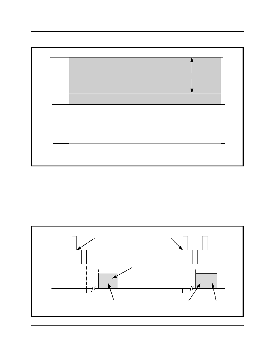
·Á
·Á
·Á
·Á
XRT7300
E3/DS3/STS-1 LINE INTERFACE UNIT
REV. 1.1.1
31
Timing Requirements associated with Declaring
and Clearing the LOS Indicator for E3 Applica-
tions
The XRT7300 was designed to meet the ITU-T G.775
specification timing requirements for declaring and
clearing the LOS indicator. In particular, the
XRT7300 declares an LOS between 10 and 255 UI
(or E3 bit-periods) after the actual time the LOS con-
dition occurred. Further, the XRT7300 clears the
LOS indicator within 10 to 255 UI after restoration of
the incoming line signal. Figure 22 illustrates the
LOS Declaration and Clearance behavior in response
to the first loss of signal event and then afterwards to
the restoration of the signal.
F
IGURE
21. T
HE
S
IGNAL
L
EVELS
THAT
THE
XRT7300 D
ECLARES
AND
C
LEARS
LOS (E3 M
ODE
O
NLY
)
0 dB
-12 dB
-15dB
-35dB
Maximum Cable Loss for E3
LOS Signal Must be Declared
LOS Signal Must be Cleared
LOS Signal may be Cleared or Declared
F
IGURE
22. T
HE
B
EHAVIOR
THE
LOS O
UTPUT
I
NDICATOR
I
N
R
ESPONSE
TO
THE
L
OSS
OF
S
IGNAL
AND
THE
R
ESTO
-
RATION
OF
S
IGNAL
Actual Occurrence
of LOS Condition
Line Signal
is Restored
Time Range for
LOS Declaration
Time Range for
LOS Clearance
G.775
Compliance
G.775
Compliance
0 UI
10 UI
0 UI
10 UI
255 UI
255 UI
RTIP/
RRing
RLOS Output Pin
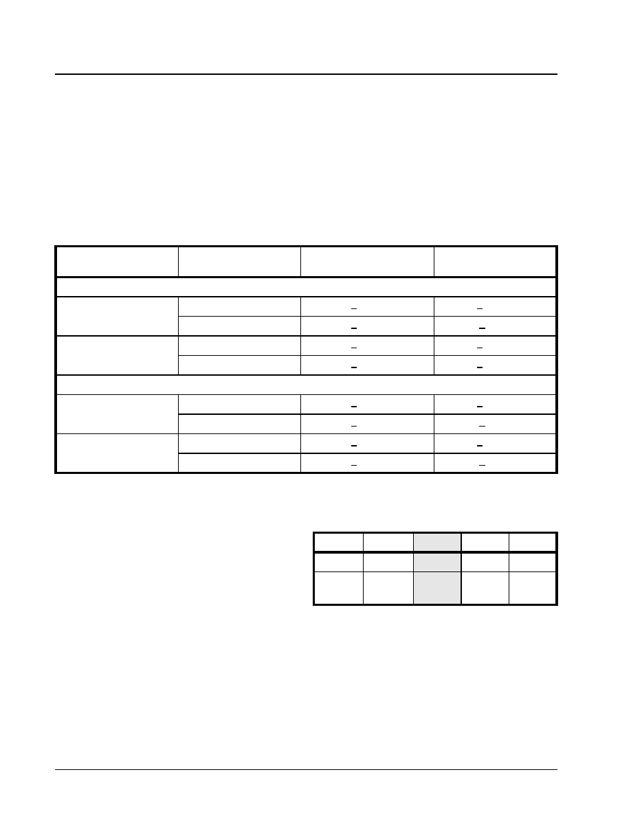
XRT7300
·Á
·Á
·Á
·Á
E3/DS3/STS-1 LINE INTERFACE UNIT
REV. 1.1.1
32
3.6.2
The LOS Declaration/Clearance Criteria
for DS3 and STS-1 Applications
When the XRT7300 is operating in the DS3 or STS-1
Modes it declares and clears LOS based on either:
∑ Analog LOS (ALOS) Declaration/Clearance Criteria
or,
∑ Digital LOS (DLOS) Declaration/Clearance Criteria
In the DS3 or STS-1 Modes the LOS output (RLOS)
is simply the logical OR of the ALOS and DLOS
states.
1. The Analog LOS (ALOS) Declaration/Clear-
ance Criteria
The XRT7300 declares an Analog LOS (ALOS) Con-
dition if the amplitude of the incoming line signal
drops below a specific amplitude as defined by the
state of the LOSTHR input pin.
Declaring ALOS
The XRT7300 declares an ALOS (Analog LOS) con-
dition whenever the amplitude of the input signal falls
below the Signal Level to Declare ALOS levels speci-
fied in Table 4.
Clearing ALOS
The XRT7300 clears ALOS whenever the amplitude
of the input signal rises above the Signal Level to
Clear ALOS levels specified in Table 4.
N
OTE
: There is approximately a 2dB hysteresis in the
received signal level that exists between declaring and
clearing ALOS in order to prevent chattering in the RLOS
output signal.
Monitoring the State of ALOS
If the XRT7300 is operating in the HOST Mode, the
state of ALOS can be polled or monitored by reading
in the contents of Command Register 0. The bit-for-
mat of Command Register 0 is presented below.
If the ALOS bit-field contains a "1", the XRT7300 is
currently declaring an ALOS condition. If the ALOS
bit-field contains a "0", the device is NOT currently de-
claring an ALOS condition.
Disabling the ALOS Detector
It is useful to disable the ALOS Detector in the
XRT7300 for debugging purposes. If the XRT7300 is
operating in the HOST Mode, the ALOS Detector can
T
ABLE
4: T
HE
ALOS D
ECLARATION
AND
C
LEARANCE
T
HRESHOLDS
FOR
A
G
IVEN
S
ETTING
OF
LOSTHR (DS3
AND
STS-1 A
PPLICATIONS
)
FOR
E
QUALIZER
E
NABLED
OR
D
ISABLED
A
PPLICATION
LOSTHR S
ETTING
S
IGNAL
L
EVEL
TO
D
ECLARE
ALOS
S
IGNAL
L
EVEL
TO
C
LEAR
ALOS
LOS L
EVEL
W
ITH
E
QUALIZER
E
NABLED
DS3
0
< 55mV
> 220mV
1
< 22mV
> 70mV
Sonet STS-1
0
< 75mV
> 270mV
1
< 25mV
> 110mV
LOS L
EVEL
W
ITH
E
QUALIZER
D
ISABLED
DS3
0
< 35mV
> 155mV
1
< 17mV
> 70mV
Sonet STS-1
0
< 55mV
> 210mV
1
< 20mV
> 90mV
COMMAND REGISTER CR0 (ADDRESS = 0X00)
D4
D3
D2
D1
D0
RLOL
RLOS
ALOS
DLOS
DMO
Read
Only
Read
Only
Read
Only
Read
Only
Read
Only
·Á
·Á
·Á
·Á
XRT7300
E3/DS3/STS-1 LINE INTERFACE UNIT
REV. 1.1.1
33
be disabled by writing a "1" into the ALOSDIS bit-field
in Command Register 2 as depicted below.
N
OTE
: Setting both the ALOSDIS and DLOSDIS bit-fields
to "1" disables LOS Declaration in the XRT7300.
2. The Digital LOS (DLOS) Declaration/Clear-
ance Criteria
The XRT7300 declare a Digital LOS (DLOS) condi-
tion if the XRT7300 detects 160±32 or more consecu-
tive "0's" in the incoming data.
The XRT7300 clears DLOS if it detects four consecu-
tive sets of 32 bit-periods each of which contains at
least 10 "1's" (e.g., average pulse density of greater
than 33%).
Monitoring the State of DLOS
If the XRT7300 is operating in the HOST Mode, the
state of DLOS can be polled or monitored by reading
in the contents of Command Register 0 as shown.
If the DLOS bit-field contains a "1", the XRT7300 is
currently declaring a DLOS condition. If the DLOS
bit-field contains a "0", the device is NOT currently de-
claring the DLOS condition.
Disabling the DLOS Detector
It is useful to disable the DLOS Detector in the
XRT7300 for debugging purposes. If the XRT7300 is
operating in the HOST Mode, the DLOS Detector can
be disabled by writing a "1" into the DLOSDIS bit-field
in Command Register 2.
N
OTE
: Setting both the ALOSDIS and DLOSDIS bit-fields
to a "1" disables LOS Declaration in the XRT7300.
3.6.3
Muting the Recovered Data while the LOS
is being Declared
In some applications it is not desirable for the
XRT7300 E3/DS3/STS-1 LIU to recover data and
route it to the Receiving Terminal while the LIU is de-
claring an LOS condition. Consequently, the
XRT7300 includes a LOS Muting feature. This fea-
ture, if enabled, causes the XRT7300 to halt trans-
mission of the recovered data to the Receiving Termi-
nal while the LOS condition is True. In this case, the
RPOS and RNEG output pins are forced to "0". Once
the LOS condition has been cleared, the XRT7300
resumes the transmission of the recovered data to
the Receiving Terminal. The XRT7300 allows en-
abling of the Muting Upon LOS feature by either of
the following means.
If the XRT7300 is Operating in the Hardware
Mode:
The Muting Upon LOS feature is enabled by pulling
the LOSMUTEN input pin (pin 19) to VDD.
If the XRT7300 is Operating in the HOST Mode:
To enable this feature, access the Microprocessor Se-
rial Interface and write a "1" into the LOSMUT bit-field
in Command Register 3.
N
OTE
: The XRT7300 automatically declares an LOS Con-
dition any time it has been configured to operate in either
the Analog Local Loop-Back or Digital Local Loop-Back
Modes. Consequently, MUTing -upon -LOS must be dis-
abled prior to configuring the device to operate in either of
these local Loop-Back modes.
3.7
R
OUTING
THE
R
ECOVERED
T
IMING
AND
D
ATA
I
NFORMATION
TO
THE
R
ECEIVING
T
ERMINAL
E
QUIPMENT
The XRT7300 ultimately takes the Recovered Timing
and Data information, converts it into CMOS levels
and routes it to the Receiving Terminal Equipment via
the RPOS, RNEG, RCLK1 and RCLK2 output pins.
The XRT7300 can deliver the recovered data and
clock information to the Receiving Terminal in either a
Single-Rail or Dual-Rail format.
Routing Dual-Rail Format Data to the Receiving
Terminal Equipment
COMMAND REGISTER CR2 (ADDRESS = 0X02)
D4
D3
D2
D1
D0
DECODIS ENCODIS ALOSDIS DLOSDIS
REQDIS
X
X
1
X
X
COMMAND REGISTER CR0 (ADDRESS = 0X00)
D4
D3
D2
D1
D0
RLOL
RLOS
ALOS
DLOS
DMO
Read
Only
Read
Only
Read
Only
Read
Only
Read
Only
COMMAND REGISTER CR2 (ADDRESS = 0X02)
D4
D3
D2
D1
D0
DECODIS ENCODIS ALOSDIS DLOSDIS
REQDIS
X
X
X
1
X
COMMAND REGISTER CR3 (ADDRESS = 0X03)
D4
D3
D2
D1
D0
RNRZ
LOSMUT
CLK2DIS RCLK2INV CLK1INV
X
1
X
X
X
XRT7300
·Á
·Á
·Á
·Á
E3/DS3/STS-1 LINE INTERFACE UNIT
REV. 1.1.1
34
Whenever the XRT7300 delivers Dual-Rail format to
the Terminal Equipment it does so via the following
output signals.
∑ RPOS
∑ RNEG
∑ RCLK1
∑ RCLK2
Figure 23 illustrates the typical interface for the trans-
mission of data in a Dual-Rail Format from the Re-
ceive Section of the XRT7300 to the Receiving Termi-
nal Equipment.
The manner that the LIU transmits Dual-Rail data to
the Receiving Terminal Equipment is described below
and illustrated in Figure 24. The XRT7300 typically
updates the data on the RPOS and RNEG output
pins on the rising edge RCLK1 (or RCLK2).
RCLK1 (or RCLK2) is the Recovered Clock signal
from the incoming Received line signal. As a result,
these clock signals are typically 34.368 MHz for E3
applications, 44.736 MHz for DS3 applications and
51.84 MHz for SONET STS-1 applications.
In general, if the XRT7300 received a positive-polarity
pulse in the incoming line signal via the RTIP and
RRING input pins, then the XRT7300 pulses the
RPOS output pin "High". If the XRT7300 received a
negative-polarity pulse in the incoming line signal via
the RTIP and RRING input pins, then the XRT7300
pulses the RNEG output pin "High".
Inverting the RCLK1 or RCLK2 outputs
When using the XRT7300, either of the RCLK1 or
RCLK2 signals can be inverted with respect to the de-
livery of the RPOS and RNEG output signals to the
Receiving Terminal Equipment. This feature may be
useful for those customers whose Receiving Terminal
Equipment logic design is such that the RPOS and
RNEG data must be sampled on the rising edge of
RCLK1 or RCLK2. Figure 25 illustrates the behavior
F
IGURE
23. T
HE
T
YPICAL
I
NTERFACE
FOR
THE
T
RANSMISSION
OF
D
ATA
IN
A
D
UAL
-R
AIL
F
ORMAT
F
ROM
THE
R
ECEIVE
S
ECTION
OF
THE
XRT7300
TO
THE
R
ECEIVING
T
ERMINAL
E
QUIPMENT
Exar E3/DS3/STS-1 LIU
Receive
Logic
Block
RxPOS
RxNEG
RCLK1, 2
RPOS
RNEG
RCLK1, 2
Terminal
Equipment
(E3/DS3 or STS-1
Framer)
F
IGURE
24. H
OW
THE
XRT7300 O
UTPUTS
D
ATA
ON
THE
RPOS
AND
RNEG O
UTPUT
P
INS
RCLK1
RPOS
RNEG
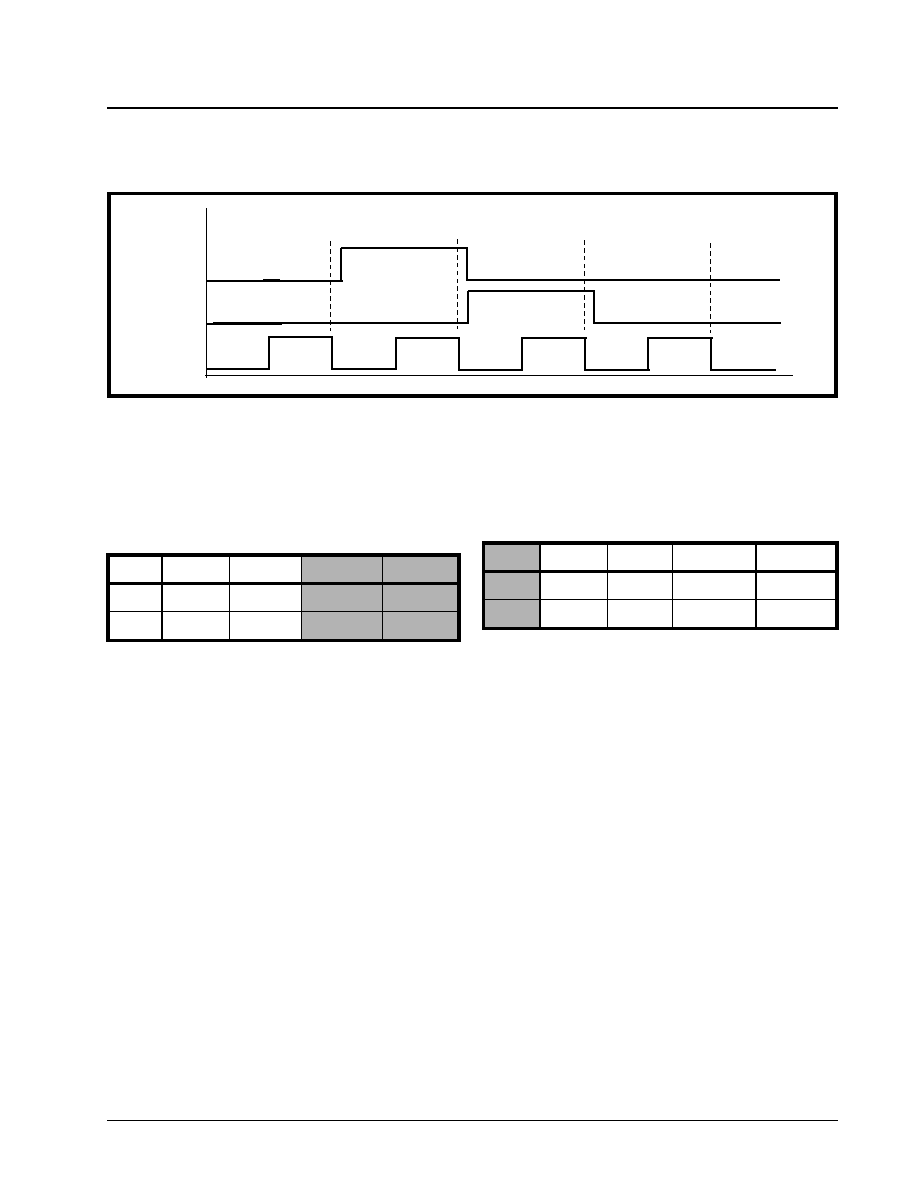
·Á
·Á
·Á
·Á
XRT7300
E3/DS3/STS-1 LINE INTERFACE UNIT
REV. 1.1.1
35
of the RPOS, RNEG and RCLK signals when the
RCLK signal has been inverted.
In order to configure the XRT7300 to invert the
RCLK1 output signal, the XRT7300 must be operat-
ing in the HOST Mode. This configuration can be im-
plemented by accessing the Microprocessor Serial
Interface block and writing a "1" into the RCLK1INV
bit-field in Command Register CR3 to invert RCLK1.
The RCLK2 output signal can also be inverted when
the XRT7300 is operating in the Hardware Mode by
setting the RCLK2INV input pin "High".
3.7.1
Routing Single-Rail Format data (Binary
Data Stream) to the Receive Terminal Equipment
To route Single-Rail format data (e.g., a binary data
stream) from the Receive Section of the XRT7300 to
the Receiving Terminal Equipment, do the following:
A. configure the XRT7300 to operate in the HOST
Mode and
B. access the Microprocessor Serial Interface and
write a "1" into the RNRZ bit-field in Command
Register CR3.
After these steps are taken, the XRT7300 outputs
Single-Rail data to the Receiving Terminal Equipment
via the RPOS and RCLK1 (or RCLK2) output pins as
illustrated in Figure 26 and Figure 27.
N
OTE
: The RNEG output pin is internally tied to Ground
whenever this feature is enabled.
F
IGURE
25. T
HE
B
EHAVIOR
OF
THE
RPOS, RNEG
AND
RCLK1 S
IGNALS
W
HEN
RCLK1
IS
I
NVERTED
RCLK1
RPOS
RNEG
COMMAND REGISTER CR3 (ADDRESS = 0X03)
D4
D3
D2
D1
D0
RNRZ
LOSMUT
CLK2DIS
RCLK2INV
RCLK1INV
X
X
X
1
1
COMMAND REGISTER CR3 (ADDRESS = 0X03)
D4
D3
D2
D1
D0
RNRZ
LOSMUT CLK2DIS
RCLK2INV
RCLK1INV
1
X
X
X
X

XRT7300
·Á
·Á
·Á
·Á
E3/DS3/STS-1 LINE INTERFACE UNIT
REV. 1.1.1
36
4.0
DIAGNOSTIC FEATURES OF THE XRT7300
The XRT7300 supports equipment diagnostic activi-
ties by supporting the following Loop-Back modes in
the chip:
∑ Analog Local Loop-Back
∑ Digital Local Loop-Back
∑ Remote Loop-Back.
4.1
T
HE
A
NALOG
L
OCAL
L
OOP
-B
ACK
M
ODE
When the XRT7300 is configured to operate in the
Analog Local Loop-Back Mode, the XRT7300 ignores
any signals that are input to the RTIP and RRING in-
put pins. The Transmitting Terminal Equipment trans-
mits clock and data into the XRT7300 via the TPDA-
TA, TNDATA and TCLK input pins. This data is pro-
cessed through the Transmit Clock Duty Cycle Adjust
PLL and the HDB3/B3ZS Encoder. Finally, this data
outputs to the line via the TTIP and TRING output
pins and is looped back into the AGC/Receive Equal-
izer Block. Consequently, this data is also processed
through the Receive Section of the XRT7300. After
this post-loop-back data has been processed through
the Receive Section it outputs to the Near-End Re-
ceiving Terminal Equipment via the RPOS, RNEG,
RCLK1 and RCLK2 output pins.
Figure 28 illustrates the path that the data takes when
the chip is configured to operate in the Analog Local
Loop-Back Mode.
The XRT7300 can be configured to operate in the An-
alog Local Loop-Back Mode by employing either one
of the following two steps:
F
IGURE
26. T
HE
T
YPICAL
I
NTERFACE
FOR
THE
T
RANSMISSION
OF
D
ATA
IN
A
S
INGLE
-R
AIL
F
ORMAT
F
ROM
THE
R
ECEIVE
S
ECTION
OF
THE
XRT7300
TO
THE
R
ECEIVING
T
ERMINAL
E
QUIPMENT
Terminal
Equipment
(E3/DS3 or STS-1
Framer)
Exar E3/DS3/STS-1 LIU
Receive
Logic
Block
RxPOS
RCLK1, 2
RPOS
RCLK1, 2
F
IGURE
27. T
HE
B
EHAVIOR
OF
THE
RPOS
AND
RCLK1 O
UTPUT
S
IGNALS
W
HILE
THE
XRT7300
IS
T
RANSMITTING
S
INGLE
-R
AIL
D
ATA
TO
THE
R
ECEIVING
T
ERMINAL
E
QUIPMENT
RCLK1
RPOS
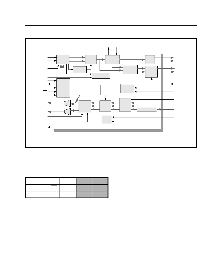
·Á
·Á
·Á
·Á
XRT7300
E3/DS3/STS-1 LINE INTERFACE UNIT
REV. 1.1.1
37
If the XRT7300 is operating in the HOST Mode:
Access the Microprocessor Serial Interface and write
a "1" into the LLB bit-field and a "0" into the RLB bit-
field in Command Register 4.
If the XRT7300 is operating in the Hardware
Mode:
The LLB input pin (pin 14) must be set to "High" and
the RLB input pin (pin 15) must be set to "Low".
N
OTES
:
1. The Analog Local Loop-Back Mode does not work
if the transmitter is turned off via the TXOFF fea-
ture.
2. The XRT7300 automatically Declares an LOS Con-
dition anytime it has been configured to operate in
either the Analog Local Loop-Back or Digital Local
Loop-Back Modes. Consequently, the MUTing -
upon -LOS must be disabled prior to configuring
the device to operate in either of these local Loop-
Back modes.
4.2
T
HE
D
IGITAL
L
OCAL
L
OOP
-B
ACK
M
ODE
When the XRT7300 is configured to operate in the
Digital Local Loop-Back Mode, it ignores any signals
that are input to the RTIP and RRING input pins. The
Transmitting Terminal Equipment transmits clock and
data into the XRT7300 via the TPDATA, TNDATA and
TCLK input pins. This data is processed through the
Transmit Clock Duty Cycle Adjust PLL and the HDB3/
B3ZS Encoder block and then looped back to the
HDB3/B3ZS Decoder block.
Figure 29 illustrates the path that the data takes when
the chip is configured to operate in the Digital Local
Loop-Back Mode.
F
IGURE
28. T
HE
A
NALOG
L
OCAL
L
OOP
-B
ACK
IN
THE
XRT7300
AGC/
Equalizer
Peak
Detector
LOS Detector
Slicer
Clock
Recovery
Data
Recovery
Invert
Loop MUX
HDB3/
B3ZS
Decoder
LOSTHR
SDI
SDO/LCV
SCLK
CS
REGRESET
RTIP
RRING
REQDIS
RCLK1
RCLK2
RPOS
RNEG
DECODIS
RLOS
LLB
RLB
ENCODIS
TAOS
TPDATA
TNDATA
TCLK
RLOL EXCLK
Device
Monitor
MTIP
MRING
Transmit
Logic
Duty Cycle Adjust
TXLEV
TXOFF
DMO
TTIP
TRING
Pulse
Shaping
HDB3/
B3ZS
Encoder
Serial
Processor
Interface
Analog Local
Loop-Back Path
COMMAND REGISTER CR4 (ADDRESS = 0X04)
D4
D3
D2
D1
D0
X
STS-1/DS3
E3
LLB
RLB
X
X
X
1
0

XRT7300
·Á
·Á
·Á
·Á
E3/DS3/STS-1 LINE INTERFACE UNIT
REV. 1.1.1
38
The Digital Local Loop-Back Mode, along with the Tx-
OFF feature, is useful in Redundancy System De-
sign. These two features permit the system to exe-
cute some diagnostic tests in the Back-up Line Card
without transmitting data onto the line and interfering
with the DS3/E3/STS-1 traffic from the Primary Line
Card.
The XRT7300 can be configured to operate in the
Digital Local Loop-Back Mode by employing either
one of the following two-steps.
A. If the XRT7300 is operating in the HOST Mode
Access the Microprocessor Serial Interface and write
a "1" into both the LLB and RLB bit-fields in Com-
mand Register 4.
B. If the XRT7300 is operating in the Hardware
Mode
Set both the LLB input pin (pin 14) and the RLB input
pin (pin 15) to "High".
N
OTES
:
1. The Digital Local Loop-Back Mode feature works
even if the transmitter is turned off via the TXOFF
feature.
2. The XRT7300 automatically declares an LOS Con-
dition any time it has been configured to operate in
either the Analog Local Loop-Back or Digital Local
Loop-Back Modes. Consequently, the MUTing -
upon -LOS must be disabled prior to configuring
the device to operate in either of these local Loop-
Back modes.
4.3
T
HE
R
EMOTE
L
OOP
-B
ACK
M
ODE
When the XRT7300 is configured to operate in the
Remote Loop-Back Mode, it ignores any signals that
are input to the TPDATA and TNDATA input pins. The
XRT7300 receives the incoming line signal via the
RTIP and RRING input pins. This data is processed
through the Receive Section of the XRT7300 and out-
puts to the Receive Terminal Equipment via the
RPOS, RNEG, RCLK1 and RCLK2 output pins. Addi-
tionally, this data is internally looped back into the
Pulse-Shaping block in the Transmit Section. At this
point, this data is routed through the remainder of the
Transmit Section of the XRT7300 and transmitted out
onto the line via the TTIP and TRING output pins.
F
IGURE
29. T
HE
D
IGITAL
L
OCAL
L
OOP
-B
ACK
PATH
IN
THE
XRT7300
AGC/
Equalizer
Peak
Detector
LOS Detector
Slicer
Clock
Recovery
Data
Recovery
Invert
Loop MUX
HDB3/
B3ZS
Decoder
LOSTHR
SDI
SDO/LCV
SCLK
CS
REGRESET
RTIP
RRING
REQDIS
RCLK1
RCLK2
RPOS
RNEG
DECODIS
RLOS
LLB
RLB
ENCODIS
TAOS
TPDATA
TNDATA
TCLK
RLOL EXCLK
Device
Monitor
MTIP
MRING
Transmit
Logic
Duty Cycle Adjust
TXLEV
TXOFF
DMO
TTIP
TRING
Pulse
Shaping
HDB3/
B3ZS
Encoder
Serial
Processor
Interface
Digital Local
Loop-Back Path
COMMAND REGISTER CR4 (ADDRESS = 0X04)
D4
D3
D2
D1
D0
X
STS-1/DS3
E3
LLB
RLB
X
X
X
1
1

·Á
·Á
·Á
·Á
XRT7300
E3/DS3/STS-1 LINE INTERFACE UNIT
REV. 1.1.1
39
Figure 30 illustrates the path that the data takes in the
XRT7300 when the chip is configured to operate in
the Remote Loop-Back Mode.
During Remote Loop-Back operation, any data which
is inputted via the RTIP and RRING input pins is also
outputted to the Terminal Equipment via the RPOS,
RNEG and RCLK output pins.
The XRT7300 can be configured to operate in the Re-
mote Loop-Back Mode by employing either one of the
following two steps
If the XRT7300 is operating in the HOST Mode:
Access the Microprocessor Serial Interface and write
a "1" into the RLB bit-field and a "0" in the LLB bit-field
in Command Register CR4.
If the XRT7300 is operating in the Hardware
Mode:
Set the RLB input pin (pin 15) to "High" and the LLB
input pin (pin 16) to "Low".
F
IGURE
30. T
HE
R
EMOTE
L
OOP
-B
ACK
P
ATH
IN
THE
XRT7300
AGC/
Equalizer
Peak
Detector
LOS Detector
Slicer
Clock
Recovery
Data
Recovery
Invert
Loop MUX
HDB3/
B3ZS
Decoder
LOSTHR
SDI
SDO/LCV
SCLK
CS
REGRESET
RTIP
RRING
REQDIS
RCLK1
RCLK2/LCV
RPOS
RNEG
DECODIS
RLOS
LLB
RLB
ENCODIS
TAOS
TPDATA
TNDATA
TCLK
RLOL EXCLK
Device
Monitor
MTIP
MRING
Transmit
Logic
Duty Cycle Adjust
TXLEV
TXOFF
DMO
TTIP
TRING
Pulse
Shaping
HDB3/
B3ZS
Encoder
Serial
Processor
Interface
Remote
Loop-Back Path
COMMAND REGISTER CR4 (ADDRESS = 0X04)
D4
D3
D2
D1
D0
X
STS-1/DS3
E3
LLB
RLB
X
X
X
0
1
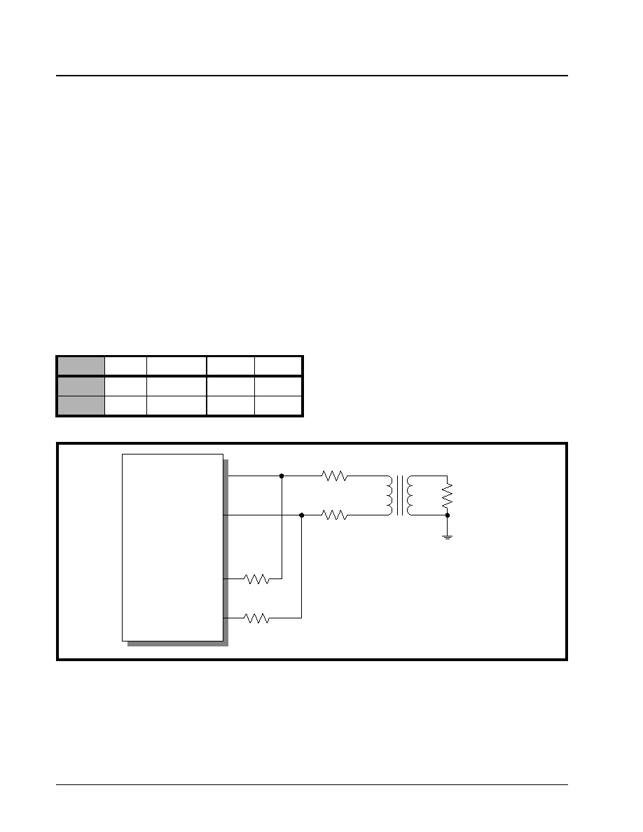
XRT7300
·Á
·Á
·Á
·Á
E3/DS3/STS-1 LINE INTERFACE UNIT
REV. 1.1.1
40
4.4
TXOFF F
EATURES
The XRT7300 allows the Transmit Driver in the Trans-
mit Section of the chip to be shut off. This feature can
be advantageous for system redundancy conditions
or during diagnostic testing. This feature can be acti-
vated by either of the following ways.
When the XRT7300 is operating in the Hardware
Mode
Shut off the Transmit Driver by toggling the TXOFF in-
put pin (pin 35) "High". Turn on the Transmit Driver by
toggling the TXOFF input pin "Low".
When the XRT7300 is operating in the HOST
Mode
If the XRT7300 is operating in the HOST Mode, the
TXOFF input pin is disabled. Consequently, the-
Transmit Driver is turned off by writing to Command
Register CR1 and setting the TXOFF bit-field (bit D4)
to "1".
N
OTE
: If the Transmitter is shut off via the TXOFF feature,
the XRT7300 can NOT be configured to operate in the Ana-
log Local Loop-Back Mode. To perform diagnostics on the
chip and still invoke the TXOFF feature as in System
Redundancy Applications, use the Digital Local Loop-Back
feature instead.
4.5
T
HE
T
RANSMIT
D
RIVE
M
ONITOR
F
EATURES
The Transmit Drive Monitor feature performs monitor-
ing of the line in the Transmit Direction for the occur-
rence of fault conditions such as a short circuit on the
line or a defective Transmit Drive in the XRT7300.
The Transmit Drive Monitor is activated by connecting
the MTIP pin (pin 44) to the TTIP line through a 270
resistor connected in series and by connecting the
MRING pin (pin 43) to the TRING line through a 270
resistor connected in series, as illustrated in
Figure 31.
When the Transmit Drive Monitor circuitry is connect-
ed to the line as illustrated in Figure 26, then it moni-
tors the line for transitions. As long as the Transmit
Drive Monitor circuitry detects transitions on the line
via the MTIP and MRING pins, it keeps the DMO
(Drive Monitor Output) signal "Low". However, if the
Transmit Drive Monitor circuit detects no transitions
on the line for 128±32 TCLK periods, then the DMO
signal toggles "High".
N
OTES
:
1. The Transmit Drive Monitor circuit does not have to
be used to operate the Transmit Section of the
XRT7300. This is purely a diagnostic feature.
COMMAND REGISTER CR1 (ADDRESS = 0X01)
D4
D3
D2
D1
D0
TXOFF
TAOS
TXCLKINV
TXLEV
TXBIN
1
X
X
X
X
F
IGURE
31. T
HE
XRT7300 E
MPLOYING
THE
T
RANSMIT
D
RIVE
M
ONITOR
F
EATURES
R1 = 36
R2 = 36
TTIP
TRING
1:1
MTIP
MRING
R3 = 270
R4 = 270
T1
R5 = 75

·Á
·Á
·Á
·Á
XRT7300
E3/DS3/STS-1 LINE INTERFACE UNIT
REV. 1.1.1
41
2. The Transmit Drive Monitor feature can also be
used to monitor the Transmit Output Line Signal of
another LIU IC as illustrated in Figure 32.
Presented in Figure 32, if LIU # 1 (U1) fails, then LIU
# 2 (U2) drives its DMO output pin "High". Likewise, if
LIU # 2 (U2) fails, then LIU # 1 (U1) drives its DMO
output pin "High".
The scheme presented in Figure 32 is a better design
approach. It overcomes situations in which a LIU
monitoring its own signal (Figure 31) may experience
a failure mode such that it cannot drive a bipolar sig-
nal onto the line. That same failure mode may pre-
vent the LIU from driving the DMO output pin "High".
4.6
T
HE
TAOS (T
RANSMIT
A
LL
O
NE
S) F
EATURE
The XRT7300 can transmit an all "1's" pattern onto
the line by toggling a single input pin or by setting a
single bit-field in one of the Command Registers to
"1".
N
OTE
: When this feature is activated, the Transmit Section
of the XRT7300 overwrites the Terminal Equipment data
with this all "1's" pattern.
This feature can be activated by either of the following
methods.
When the XRT7300 is operating in the Hardware
Mode:
Configure the device to transmit an all "1's" pattern by
toggling the TAOS input pin (pin 2) "High". Terminate
the all "1's" pattern by toggling the TAOS input pin
"Low".
When the XRT7300 is operating in the HOST
Mode:
If the XRT7300 is operating in the HOST Mode, the
TAOS input pin is disabled. Consequently, the
XRT7300 can be configured to transmit an all "1's"
pattern by writing to Command Register CR1 and set-
ting the TAOS bit-field (bit D3) to "1".
The all "1's" pattern can be terminated by writing to
Command Register CR1 and setting the TAOS bit-
field (D3) to "0".
F
IGURE
32. T
WO
LIU'
S
, E
ACH
M
ONITORING
THE
T
RANSMIT
O
UTPUT
S
IGNAL
OF
THE
O
THER
LIU IC
R1
36
BNC
T1
R2
36
R7
36
BNC
R8
36
TTIP
TRING
R3
270
R4
270
R5
270
R6
270
TRING
TTIP
MRING
MTIP
MRING
MTIP
DMO_Channel_2
DMO_Channel_1
DMO
DMO
T2
PE-68629
PE-68629
TXOFF
TXOFF
U1
U2
COMMAND REGISTER CR1 (ADDRESS = 0X01)
D4
D3
D2
D1
D0
TXOFF
TAOS
TXCLKINV
TXLEV
TXBIN
0
1
X
X
X

XRT7300
·Á
·Á
·Á
·Á
E3/DS3/STS-1 LINE INTERFACE UNIT
REV. 1.1.1
42
5.0
THE MICROPROCESSOR SERIAL INTER-
FACE
The on-chip Command Registers of the XRT7300
DS3/E3/STS-1 Line Interface Unit IC are accessed to
configure the XRT7300 into a variety of modes. This
section describes the Command Registers and how
to use the Microprocessor Serial Interface.
5.1
D
ESCRIPTION
OF
THE
C
OMMAND
R
EGISTERS
A listing of these Command Registers, their Address-
es and their Bit-Formats are listed in Table 5.
Address:
The register addresses are in Hexadecimal format.
Type:
The Command Registers are either Read-Only (RO)
or Read/Write (R/W) registers.
N
OTES
:
1. The default value for each of the bit-fields in these
registers is "0".
2. If the REGRESET input pin is asserted, then the
contents of the command registers is reset to all
"0's" resulting in the XRT7300 operating in the
mode corresponding to the default values of the
Command Registers.
DESCRIPTION OF BIT-FIELDS FOR EACH COM-
MAND REGISTER
5.1.1
Command Register - CR0
Bit D4 - RLOL (Receive Loss of Lock Status)
This Read-Only bit-field reflects the lock status of the
Clock Recovery Phase-Locked-Loop in the XRT7300.
This bit-field is set to "0" if the Clock Recovery PLL is
in lock with the incoming line signal. This bit-field is
set to "1" if the Clock Recovery PLL is out of lock with
the incoming line signal.
Bit D3 - RLOS (Receive Loss of Signal Status)
This Read-Only bit-field indicates whether or not the
Receiver in the XRT7300 is currently declaring an
LOS (Loss of Signal) Condition.
This bit-field is set to "0" if the XRT7300 is not cur-
rently declaring the LOS Condition. This bit-field is
set to "1" if the XRT7300 is declaring an LOS Condi-
tion.
Bit D2 - ALOS (Analog Loss of Signal Status)
T
ABLE
5: A
DDRESSES
AND
B
IT
F
ORMATS
OF
XRT7300 C
OMMAND
R
EGISTERS
A
DDRESS
C
OMMAND
R
EGISTER
T
YPE
R
EGISTER
B
IT
-F
ORMAT
D4
D3
D2
D1
D0
0x00
CR0
RO
RLOL
RLOS
ALOS
DLOS
DMO
0x01
CR1
R/W
TXOFF
TAOS
TXCLKINV
TXLEV
TXBIN
0x02
CR2
R/W
DECODIS
ENCODIS
ALOSDIS
DLOSDIS
REQDIS
0x03
CR3
R/W
RNRZ
LOSMUT
RCLK2/LCV
RCLK2INV
RCLK1INV
0x04
CR4
R/W
Reserved
STS-1/DS3
E3
LLB
RLB
0x05
CR5
R/W
Reserved
Reserved
Reserved
Reserved
Reserved
0x06
CR6
R/W
Reserved
Reserved
Reserved
Reserved
Reserved
0x07
CR7
R/W
Reserved
Reserved
Reserved
Reserved
Reserved
0x08
CR8
R/W
Reserved
Reserved
Reserved
Reserved
Reserved
0x09
CR9
R/W
Reserved
Reserved
Reserved
Reserved
Reserved
0x10
CR10
R/W
Reserved
Reserved
Reserved
Reserved
Reserved
0x11
CR11
R/W
Reserved
Reserved
Reserved
Reserved
Reserved
0x12
CR12
R/W
Reserved
Reserved
Reserved
Reserved
Reserved
0x13
CR13
R/W
Reserved
Reserved
Reserved
Reserved
Reserved
0x14
CR14
R/W
Reserved
Reserved
Reserved
Reserved
Reserved
0x15
CR15
R/W
Reserved
Reserved
Reserved
Reserved
Reserved

·Á
·Á
·Á
·Á
XRT7300
E3/DS3/STS-1 LINE INTERFACE UNIT
REV. 1.1.1
43
This Read-Only bit-field indicates whether or not the
Analog LOS Detector in the XRT7300 is currently de-
claring an LOS condition.
This bit-field is set to "0" if the Analog LOS Detector in
the XRT7300 is NOT currently declaring an LOS con-
dition. Conversely, this bit-field is set to "1" if the Ana-
log LOS Detector is currently declaring an LOS condi-
tion.
The purpose of this feature is to isolate either the An-
alog LOS or the Digital LOS detector that is declaring
the LOS condition. This feature may be useful for
troubleshooting/debugging purposes.
Bit D1 - DLOS (Digital Loss of Signal Status)
This Read-Only bit-field indicates whether or not the
Digital LOS Detector in the XRT7300 is currently de-
claring an LOS condition.
This bit-field is set to "0" if the Digital LOS Detector in
the XRT7300 is NOT currently declaring an LOS con-
dition. Conversely, this bit-field is set to "1" if the Digi-
tal LOS Detector is currently declaring an LOS condi-
tion.
N
OTE
: The purpose of this feature is to isolate the Detector
(e.g., either the Analog LOS or the Digital LOS detector)
that is declaring the LOS condition. This feature may be
useful for troubleshooting/debugging purposes.
Bit D0 - DMO (Drive Monitor Output Status)
This Read-Only bit-field reflects the status of the
DMO output pin.
5.1.2
Command Register - CR1
Bit D4 - TXOFF (Transmitter OFF)
This Read/Write bit-field is used to turn off the Trans-
mitter in the XRT7300.
Writing a "1" to this bit-field turns off the Transmitter
and tri-states the Transmit Output. Writing a "0" to
this bit-field turns on the Transmitter.
Bit D3 - TAOS (Transmit All OneS)
This Read/Write bit-field is used to command the
XRT7300 Transmitter to generate and transmit an all
"1's" pattern onto the line.
Writing a "1" to this bit-field commands the Transmit-
ter to transmit an all "1's" pattern onto the line. Writ-
ing a "0" to this bit-field commands normal operation.
Bit D2 - TXCLKINV (Transmit Clock Invert)
This Read/Write bit-field is used to configure the
XRT7300 Transmitter to sample the signal at the TP-
DATA and TNDATA pins on the rising or falling edge of
TCLK (the Transmit Line Clock signal).
Writing a "1" to this bit-field configures the Transmitter
to sample the TPDATA and TNDATA input pins on the
rising edge of TCLK. Writing a "0" to this bit-field con-
figures the Transmitter to sample the TPDATA and
TNDATA input pins on the falling edge of TCLK.
Bit D1 - TXLEV (Transmit Level Select)
This Read/Write bit-field is used to enable or disable
the XRT7300 Transmit Line Build-Out circuit.
Setting this bit-field "High" disables the Line Build-Out
circuit of the XRT7300. In this mode, the XRT7300
outputs partially-shaped pulses onto the line via the
TTIP and TRING output pins. Setting this bit-field
"Low" enables the Line Build-Out circuit of the
XRT7300. In this mode the XRT7300 outputs shaped
pulses onto the line via the TTIP and TRING output
pins.
To comply with the Isolated DSX/STSX-1 Pulse Tem-
plate Requirements per Bellcore GR-499-CORE or
GR-253-CORE, either:
1. set this input pin to "1" if the cable length between
the Cross-Connect and the transmit output of the
XRT7300 is greater than 225 feet or
2. set this input pin to "0" if the cable length between
the Cross-Connect and the transmit output of the
XRT7300 is less than 225 feet.
N
OTE
: This option is only available when the XRT7300 is
operating in the DS3 or STS-1 Mode.
Bit D0 - TXBIN (Transmit Binary Data)
This Read/Write bit-field permits configuring of the
Transmitter in the XRT7300 to accept an un-encoded
binary data stream via the TPDATA input and con-
verts this data into the appropriate bipolar signal to
the line.
Writing a "1" configures the Transmitter to accept a bi-
nary data stream via the TPDATA input.
N
OTE
: The TNDATA input is ignored.
This form of data acceptance is sometimes referred
to as Single-Rail mode operation. The Transmitter
then encodes this data into the appropriate line code
(e.g., B3ZS or HDB3) prior to its transmission over
the line.
Writing a "0" configures the Transmitter to accept data
in a Dual-Rail manner (e.g., via both the TPDATA and
TNDATA inputs).

XRT7300
·Á
·Á
·Á
·Á
E3/DS3/STS-1 LINE INTERFACE UNIT
REV. 1.1.1
44
5.1.3
Command Register - CR2
Bit D4 - DECODIS (B3ZS/HDB3 Decoder-Disable)
This Read/Write bit-field is used to either enable or
disable the B3ZS/HDB3 Decoder in the XRT7300.
Writing a "1" to this bit-field disables the B3ZS/HDB3
Decoder. Writing a "0" to this bit-field enables the
B3ZS/HDB3 Decoder.
N
OTE
: This Decoder performs HDB3 Decoding if the
XRT7300 is operating in the E3 Mode. Otherwise it per-
forms B3ZS Decoding.
Bit D3 - ENCODIS (B3ZS/HDB3 Encoder-Disable)
This Read/Write bit-field is used to enable or disable
the B3ZS/HDB3 Encoder in the XRT7300.
Writing a "1" to this bit-field disables the B3ZS/HDB3
Encoder. Writing a "0" to this bit-field enables the
B3ZS/HDB3 Encoder.
N
OTE
: This Encoder performs HDB3 Encoding if the
XRT7300 is operating in the E3 Mode. Otherwise, it per-
forms B3ZS Encoding.
Bit D2 - ALOSDIS (Analog LOS Disable)
This Read/Write bit-field is used to disable the Analog
LOS Detector.
Writing a "0" to this bit-field enables the Analog LOS
Detector. Writing a "1" to this bit-field disables the
Analog LOS Detector.
N
OTE
: If the Analog LOS Detector is disabled, then the
RLOS input pin is only asserted by the DLOS (Digital LOS
Detector).
Bit D1 - DLOSDIS (Digital LOS Disable)
This Read/Write bit-field is used to disable the Digital
LOS Detector.
Writing a "0" to this bit-field enables the Digital LOS
Detector. Writing a "1" to this bit-field disables the
Digital LOS Detector.
N
OTE
: If the Digital LOS Detector is disabled, then the
RLOS input pin is only asserted by the ALOS (Analog LOS
Detector).
Bit D0 - REQDIS (Receive Equalization Disable)
This Read/Write bit-field is used to either enable or
disable the internal Receive Equalizer in the
XRT7300.
Writing a "0" to this bit-field enables the Internal
Equalizer. Writing a "1" to this bit-field disables the
Internal Equalizer.
5.1.4
Command Register - CR3
Bit D4 - RNRZ (Receive Binary Data)
This Read/Write bit-field is used to configure the
XRT7300 to output the received data from the Re-
mote Terminal in a binary or Dual-Rail format.
Writing a "1" to this bit-field configures the XRT7300
to output data to the Terminal Equipment in a Single-
Rail (binary) format via the RPOS output pin. The
RNEG is grounded. A "0" to this bit-field configures
the XRT7300 to output data to the Terminal Equip-
ment in a Dual-Rail format via both the RPOS and
RNEG output pins.
Bit D3 - LOSMUT (Recovered Data MUTing during
LOS Condition)
This Read/Write bit-field is used to configure the
XRT7300 to NOT output any recovered data while it is
declaring an LOS condition to the terminal equip-
ment.
Writing a "0" to this bit-field configures the chip to out-
put recovered data even while the XRT7300 is declar-
ing an LOS condition. Writing a "1" to this bit-field
configures the chip to NOT output the recovered data
while an LOS condition is being declared.
N
OTE
: In this mode, RPOS and RNEG is set to "0" asyn-
chronously.
Bit D2 - RCLK2/LCV (Receive Clock Output 2/Line
Code Violation)
This Read/Write bit-field is used to select the function
of pin 30 (RCLK2/LCV). Pin 30 can be configured to
function as the Line Code Violation output indicator or
as the additional Receive Clock Output (RCLK2).
Writing a "0" to this bit-field configures the pin to func-
tion as the Line Code Violation output pin. Writing a
"1" to this bit-field configures this pin to function as
the RCLK2 output pin.
Bit D1 - RCLK2INV (Invert RCLK2)
This Read/Write bit-field is used to configure the Re-
ceiver in the XRT7300 to output the recovered data
on either the rising edge or the falling edge of the
RCLK2 clock signal.
Writing a "0" to this bit-field configures the Receiver to
output the recovered data on the rising edge of the
RCLK2 output signal. Writing a "1" to this bit-field
configures the Receiver to output the recovered data
on the falling edge of the RCLK2 output signal.
Bit D0 - RCLK1INV (Invert RCLK1)
This Read/Write bit-field is used to configure the Re-
ceiver in the XRT7300 to output the recovered data
on either the rising edge or the falling edge of the
RCLK1 clock signal.
Writing a "0" to this bit-field configures the Receiver to
output the recovered data on the rising edge of the
RCLK1 output signal. Writing a "1" to this bit-field
configures the Receiver to output the recovered data
on the falling edge of the RCLK1 output signal.

·Á
·Á
·Á
·Á
XRT7300
E3/DS3/STS-1 LINE INTERFACE UNIT
REV. 1.1.1
45
5.1.5
Command Register - CR4
Bit D4 - Reserved
This bit-field has no defined functionality
Bit D3 - STS-1/DS3 Mode Select
This Read/Write bit-field is used to configure the
XRT7300 to operate in either the SONET STS-1
Mode or the DS3 Mode.
Writing a "0" into this bit-field configures the XRT7300
to operate in the DS3 Mode. Writing a "1" into this bit-
field configures the XRT7300 to operate in the SO-
NET STS-1 Mode.
N
OTE
: This bit-field is ignored if the E3 bit-field (D2 in this
Command Register) is set to "1".
Bit D2 - E3 Mode Select
This Read/Write bit-field is used to configure the
XRT7300 to operate in the E3 Mode.
Writing a "0" into this bit-field configures the XRT7300
to operate in either the DS3 or SONET STS-1 Mode
specified by the setting of the DS3 bit-field in this
Command Register. Writing a "1" into this bit-field
configures the XRT7300 to operate in the E3 Mode.
Bit D1 - LLB (Local Loop-Back)
This Read/Write bit-field along with RLB (bit D0 in this
Command Register) is used to select which Loop-
Back mode the XRT7300 operates in. Table 6 relates
the state of the LLB and RLB to the selected Loop-
Back mode.
Bit D0 - RLB (Remote Loop-Back)
This Read/Write bit-field along with LLB (bit D1 in this
Command Register) is used to select which Loop-
Back mode the XRT7300 operate in. Table 6 relates
the state of the LLB and RLB bits to the selected
Loop-Back mode.
5.2
O
PERATING
THE
M
ICROPROCESSOR
S
ERIAL
I
NTERFACE
.
The XRT7300 Serial Interface is a simple four wire in-
terface that is compatible with many of the microcon-
trollers available in the market. This interface con-
sists of the following signals:
CS
-
Chip Select (Active Low)
SCLK
-
Serial Clock
SDI
-
Serial Data Input
SDO
-
Serial Data Output
Using the Microprocessor Serial Interface
The following instructions for using the Microproces-
sor Serial Interface are best understood by referring
to the diagram in Figure 33.
In order to use the Microprocessor Serial Interface, a
clock signal must be supplied to the SCLK input pin.
A Read or Write operation can then be initiated by as-
serting the active-low Chip Select input pin (CS). It is
important to assert the CS pin (e.g., toggle it "Low") at
least 50ns prior to the very first rising edge of the
clock signal.
Once the CS input pin has been asserted, the type of
operation and the target register address must now
be specified. This information is supplied to the Mi-
croprocessor Serial Interface by writing eight serial
bits of data into the SDI input.
N
OTE
: Each of these bits is clocked into the SDI input on
the rising edge of SCLK. These eight bits are identified and
described below.
Bit 1 - R/W (Read/Write) Bit
This bit is clocked into the SDI input on the first rising
edge of SCLK after CS has been asserted. This bit
indicates whether the current operation is a Read or
Write operation. A "1" in this bit specifies a Read op-
eration, a "0" in this bit specifies a Write operation.
Bits 2 through 5: The four (4) bit Address Values
(labeled A0, A1, A2 and A3)
The next four rising edges of the SCLK signal clock in
the 4-bit address value for this particular Read (or
Write) operation. The address selects the Command
Register in the XRT7300 that the user is either read-
ing data from or writing data to. The address bits
must be supplied to the SDI input pin in ascending or-
der with the LSB (least significant bit) first.
Bits 6 and 7:
The next two bits, A4 and A5 must be set to "0" as
shown in Figure 33.
Bit 8:
The value of A6 is a "don't care".
T
ABLE
6: L
OOP
-B
ACK
M
ODES
LLB
(B
IT
D1)
RLB
(B
IT
D0)
L
OOP
-B
ACK
M
ODE
0
0
No Loop-Back Mode (Normal
Operation)
0
1
Remote Loop-Back Mode
1
0
Analog Loop-Back Mode
1
1
Digital Loop-Back Mode
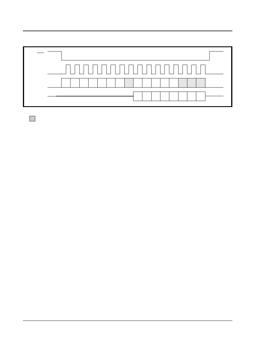
XRT7300
·Á
·Á
·Á
·Á
E3/DS3/STS-1 LINE INTERFACE UNIT
REV. 1.1.1
46
Figure 34 illustrates how to interface the XRT7300 to
the XRT7234/45 E3/DS3 ATM UNI IC.
For more information on the XRT7234 E3 UNI or the
XRT7245 DS3 UNI IC's please consult the XRT7234
E3 UNI IC or the XRT7245 DS3 UNI IC Data Sheets.
F
IGURE
33. M
ICROPROCESSOR
S
ERIAL
I
NTERFACE
D
ATA
S
TRUCTURE
D0
D1
D2
D7
D6
D5
D4
D3
High Z
S D O
A0
D0
R/W
D1
A6
0
0
A3
A2
A1
D7
D6
D5
D4
D3
D2
SDI
1
2
3
4
5
6
7
8
9
10
11
12
13
14
15
16
SClk
CS
High Z
- Denotes a "don't care" value
A4 and A5 are always "0".
R/W = "1" for "Read" Operations
R/W = "0" for "Write" Operations
Notes:
- Denotes a "don't care" value
A4 and A5 are always "0".
R/W = "1" for "Read" Operations
R/W = "0" for "Write" Operations
Notes:
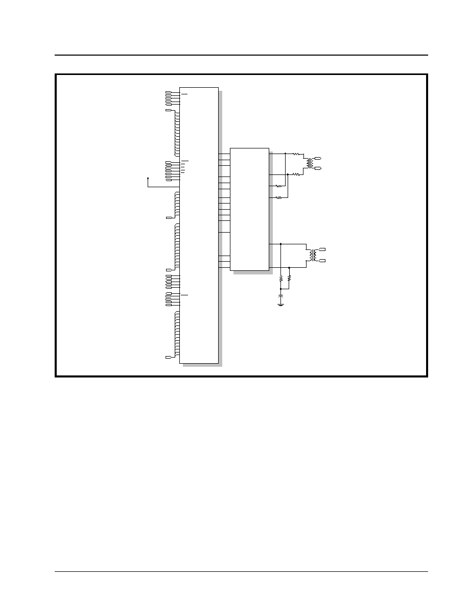
·Á
·Á
·Á
·Á
XRT7300
E3/DS3/STS-1 LINE INTERFACE UNIT
REV. 1.1.1
47
F
IGURE
34. H
OW
TO
I
NTERFACE
THE
XRT7300 IC
TO
THE
XRT7234/45 E3/DS3 ATM UNI IC
TxSoC
TxEnB
TxClk
TxPrty
TxClav
TxData0
TxData1
TxData2
TxData3
TxData4
TxData5
TxData6
TxData7
TxData8
TxData9
TxData10
TxData11
TxData12
TxData13
TxData14
TxData15
RESET
INT
CS
WR_RW
RD_DS
ALE_AS
Rdy_Dtck
MOTO
A0
A1
A2
A3
A4
A5
A6
A7
A8
D0
D1
D2
D3
D4
D5
D6
D7
D8
D9
D10
D11
D12
D13
D14
D15
RxLOS
RxOOF
RxLCS
RxRED
RxAIS
RxSOC
RxEnB
RxCLk
RxPrty
RxClav
RxData0
RxData1
RxData2
RxData3
RxData4
RxData5
RxData6
RxData7
RxData8
RxData9
RxData10
RxData11
RxData12
RxData13
RxData14
RxData15
TxSoC
TxEnB
TxClk
TxPrty
TxClav
TxData [15:0]
RESET
INT
CS
RW
DS
AS
DTACK
A[8:0]
D[15:0]
RxLOS
RxOOF
RxLCS
RxRED
RxAIS
RxSOC
RxEnB
RxCLk
RxPrty
RxClav
RxData[15:0]
TxPOS
TxNEG
TxLineClk
DMO
ExLOS
RLOL
LLOOP
RLOOP
TAOS
TxLEV
ENCODIS
REQB
RxPOS
RxNEG
RxLineClk
TPDATA
TNDATA
TCLK
DMO
RLOS
RLOL
LLB
RLB
TAOS
TxLEV
ENCODIS
REQDIS
RPOS
RNEG
RCLK1
TTIP
TRING
MTIP
MRING
RTIP
RRING
R4
270
R3
270
T1
R1
36
R2
36
1:1
TTIP
TRING
T2
1:1
RTIP
RRING
R5
37.5
R6
37.5
0.01uF
C1
+5V
XRT7245
XRT7300
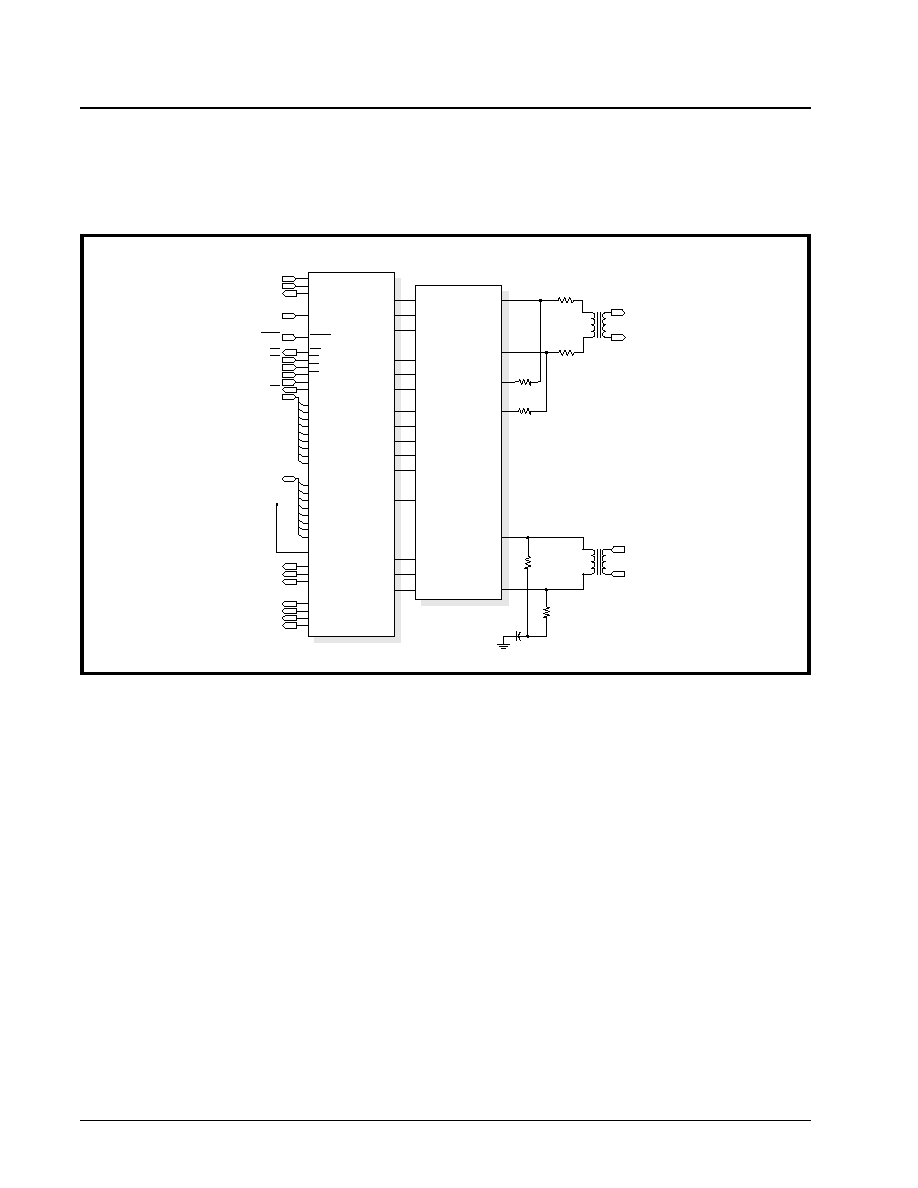
XRT7300
·Á
·Á
·Á
·Á
E3/DS3/STS-1 LINE INTERFACE UNIT
REV. 1.1.1
48
Figure 35 illustrates how to interface the XRT7300 to
the XRT7250 E3/DS3 Framer IC. Please note that in
this case, the XRT7300 has been configured to oper-
ate in the Hardware Mode.
For more information on the XRT7250 E3/DS3 Fram-
er IC's please consult the XRT7250 E3/DS3 Framer
IC Data Sheet.
F
IGURE
35. H
OW
TO
I
NTERFACE
THE
XRT7300 IC
TO
THE
XRT7250 DS3/E3 F
RAMER
IC
TxSER
TXInClk
TxFrame
NIBBLEINTF
RESET
INT
CS
RW
DS
AS
INT
A[8:0]
D[7:0]
5V
RxSer
RxClk
RxFrame
RxLOS
RxOOF
RxRED
RxAIS
TxSER
TXInClk
TxFrame
NIBBLEINTF
RESET
INT
CS
WR_RW
RD_DS
ALE_AS
Rdy Dtck
A0
A1
A2
A3
A4
A5
A6
A7
A8
D0
D1
D2
D3
D4
D5
D6
D7
MOTO
RxSer
RxClk
RxFrame
RxLOS
RxOOF
RxRED
RxAIS
TxPOS
TxNEG
TxLineClk
DMO
ExtLOS
RLOL
LLOOP
RLOOP
TAOS
TxLEV
ENCODIS
REQB
RxPOS
RxNEG
RxLineClk
XRT7250
TPDATA
TNDATA
TCLK
DMO
RLOS
RLOL
LLB
RLB
TAOS
TXLEV
ENCODIS
REQDIS
RPOS
RNEG
RCLK1
TTIP
TRING
MTIP
MRING
RTIP
RRING
R4
270
R3
270
T1
R1
36
R2
36
1:1
TTIP
TRING
T2
1:1
RTIP
RRING
R5
37.5
R6
37.5
0.01uF
C1
XRT7300

·Á
·Á
·Á
·Á
XRT7300
E3/DS3/STS-1 LINE INTERFACE UNIT
REV. 1.1.1
49
ORDERING INFORMATION
PACKAGE DIMENSIONS
P
ART
N
O
.
P
ACKAGE
O
PERATING
T
EMPERATURE
R
ANGE
XRT7300IV
44 Pin TQFP (10mm x 10mm)
-40∞C to +85∞C
33
23
22
12
1
11
34
44
D
D
1
D
D
1
B
e
A
2
A
1
A
Seating Plane
L
C
44 LEAD THIN QUAD FLAT PACK
(10 x 10 x 1.4 mm TQFP)
rev. 1.00
Note: The control dimension is the millimeter column
S Y M B O L
M I N
M A X
M I N
M A X
A
0.055
0.063
1.4
1.6
A 1
0.002
0.006
0.05
0.15
A 2
0.053
0.057
1.35
1.45
B
0.012
0.018
0.3
0.45
C
0.004
0.008
0.09
0.2
D
0.465
0.48
11.8
12.2
D 1
0.39
0.398
9.9
10.1
e
L
0.018
0.03
0.45
0.75
0
o
7
o
0
o
7
o
I N C H E S
M I L L I M E T E R S
0.0315 BSC
0.80 BSC

XRT7300
·Á
·Á
·Á
·Á
E3/DS3/STS-1 LINE INTERFACE UNIT
REV. 1.1.1
50
REVISION HISTORY
Rev. 1.0.0 original
Rev. 1.0.1 page 12 Leackage Current Units from mA
to µA
Rev. 1.0.2 edits to missing symbols
Rev. 1.0.3 changes to Notes for Analog and Digital
Loop-Back modes and added ESD Rating
Rev. 1.0.4 and 1.0.5 Added REQDIS to block dia-
gram; renamed REG_RESET* to REGRESET, CS* to
CS, ICT* to ICT, HOST/HW* to HOST/HW, STS-1/
DS3* to STS-1/DS3; changed format/style of the data
sheetand removed uneccessary verbage; added ta-
ble of contents. Modified figures 3 & 4 for complet-
ness.
Rev. 1.0.7 added Device Monitor function to block di-
agram, changed figure 22, RxIN to RTIP/RRING.
Rev. 1.1.0 Electrical tables incorrectly stated 3.3V re-
placed with 5.0V, Rev # made consistent with produc-
tion products.
Rev 1.1.1 Added connection points to various draw-
ings.

·Á
·Á
·Á
·Á
XRT7300
E3/DS3/STS-1 LINE INTERFACE UNIT
REV. 1.1.1
51
NOTICE
EXAR Corporation reserves the right to make changes to the products contained in this publication in order
to improve design, performance or reliability. EXAR Corporation assumes no responsibility for the use of
any circuits described herein, conveys no license under any patent or other right, and makes no represen-
tation that the circuits are free of patent infringement. Charts and schedules contained here in are only for
illustration purposes and may vary depending upon a user's specific application. While the information in
this publication has been carefully checked; no responsibility, however, is assumed for inaccuracies.
EXAR Corporation does not recommend the use of any of its products in life support applications where
the failure or malfunction of the product can reasonably be expected to cause failure of the life support sys-
tem or to significantly affect its safety or effectiveness. Products are not authorized for use in such applica-
tions unless EXAR Corporation receives, in writing, assurances to its satisfaction that: (a) the risk of injury
or damage has been minimized; (b) the user assumes all such risks; (c) potential liability of EXAR Corpo-
ration is adequately protected under the circumstances.
Copyright 2001 EXAR Corporation
Datasheet February 2002.
Reproduction, in part or whole, without the prior written consent of EXAR Corporation is prohibited.