EXAR Corporation, 48720 Kato Road, Fremont, CA 94538
∑
(510) 668-7000
∑
FAX (510) 668-7017
ST16C654/654D
Rev. 4.30
PLCC Package
9
8
7
6
5
4
3
2
1
68
67
66
65
64
63
62
63
10
11
12
13
14
15
16
17
18
19
20
21
22
23
24
25
26
60
59
58
57
56
55
54
53
52
51
50
49
48
47
46
45
44
27
28
29
30
31
32
33
34
35
36
37
38
39
40
41
42
43
-DSRA
-CTSA
-DTRA
VCC
-RTSA
INTA
-CSA
TXA
-IOW
TXB
-CSB
INTB
-RTSB
GND
-DTRB
-CTSB
-DSRB
-C
D
B
-R
I
B
RX
B
CLK
SEL
16/
-
6
8
A2
A1
A0
XT
AL
1
XT
AL
2
RE
S
E
T
-R
X
R
D
Y
-
T
X
RDY
GND
RX
C
-R
I
C
-C
D
C
-DSRD
-CTSD
-DTRD
GND
-RTSD
INTD
-CSD
TXD
-IOR
TXC
-CSC
INTC
-RTSC
VCC
-DTRC
-CTSC
-DSRC
-C
D
A
-R
I
A
RX
A
GND
D7
D6
D5
D4
D3
D2
D1
D0
IN
T
S
E
L
VC
C
RX
D
-R
I
D
-C
D
D
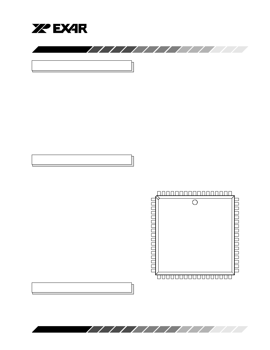
ST16C654CJ68
16 MODE
QUAD UART WITH 64-BYTE FIFO AND
INFRARED (IrDA) ENCODER/DECODER
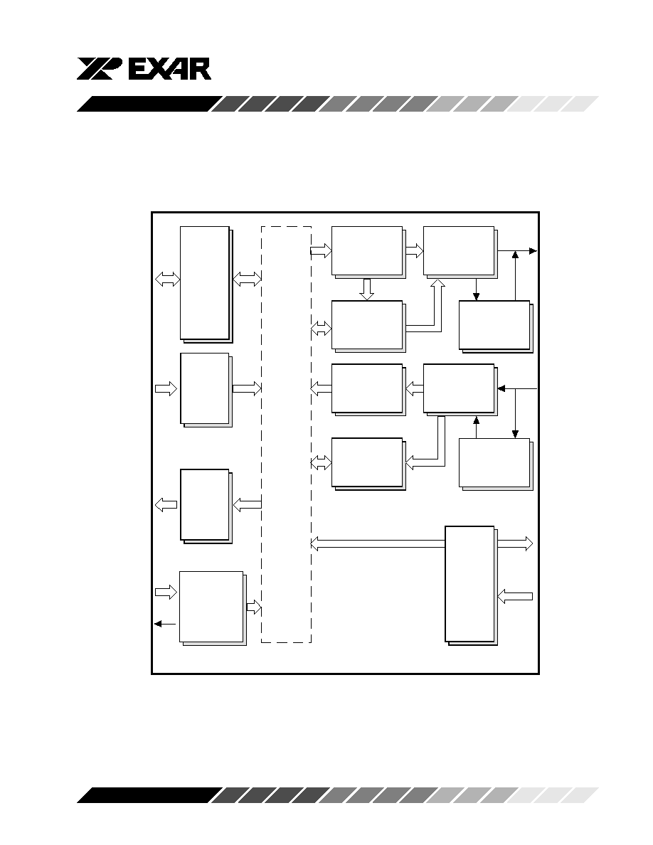
DESCRIPTION
The ST16C654 *
1
is a universal asynchronous receiver and transmitter (UART) with a dual foot print interface
compatible with the ST16C554 and ST68C554. The 654 is an enhanced UART with 64 byte FIFOs, automatic
hardware/software flow control, and data rates up to 1.5Mbps. Onboard status registers provide the user with error
indications and operational status, modem interface control. System interrupts may be tailored to meet user
requirements. An internal loop-back capability allows onboard diagnostics. The 654 is available in 64 pin TQFP,
68 pin PLCC, and 100 pin QFP packages. The 64 pin package offers the 16 interface mode which is compatible
with the industry standard ST16C554. The 68 and 100 pin packages offer an additional 68 mode which allows easy
integration with Motorola, and other popular microprocessors. The ST16C654CQ64 (64 pin) offers three state
interrupt control while the ST16C654DCQ64 provides constant active interrupt outputs. The 64 pin devices do
not offer TXRDY/RXRDY outputs or the default clock select option (CLKSEL). The 100 pin packages offer faster
channel status access by providing separate outputs for TXRDY and RXRDY, offer separate Infrared TX outputs
and a musical instrument clock input (MIDICLK). The 654 combines the package interface modes of the 16C454/
554 and 68/C454/554 series on a single integrated chip.
FEATURES
∑
Compatibility with the Industry Standard
ST16C454/554, ST68C454/554, TL16C554
∑
1.5 Mbps transmit/receive operation (24MHz)
∑
64 byte transmit FIFO
∑
64 byte receive FIFO with error flags
∑
Automatic software/hardware flow control
∑
Programmable Xon/Xoff characters
∑
Independent transmit and receive control
∑
Software selectable Baud Rate Generator pre-
scaleable clock rates of 1X, 4X.
∑
Four selectable Transmit/Receive FIFO interrupt
trigger levels
∑
Standard modem interface or infrared IrDA en-
coder/decoder interface
∑
Software flow control turned off optionally by any
(Xon) RX character
∑
Independent MIDI interface on 100 pin packages
∑
100 pin packages offer internal register FIFO
monitoring and separate IrDA TX outputs
∑
Sleep mode ( 200mA stand-by)
ORDERING INFORMATION
Part number
Pins Package Operating temperature
ST16C654CJ68
68
PLCC
0∞ C to + 70∞ C
ST16C654CQ64
64
TQFP
0∞ C to + 70∞ C
ST16C654DCQ64 64
TQFP
0∞ C to + 70∞ C
ST16C654CQ100 100 QFP
0∞ C to + 70∞ C
Part number
Pins Package Operating temperature
ST16C654IJ68
68
PLCC
-40∞ C to + 85∞ C
ST16C654IQ64
64
TQFP
-40∞ C to + 85∞ C
ST16C654DIQ64
64
TQFP
-40∞ C to + 85∞ C
ST16C654IQ100
100 QFP
-40∞ C to + 85∞ C
Note *1: Patent Pending
ST16C654/654D
5
Rev. 4.30
SYMBOL DESCRIPTION
Symbol
Pin
Signal
Pin Description
68
100
64
type
16/-68
31
36
-
I
16/68 Interface Type Select (input with internal pull-up). -
This input provides the 16 (Intel) or 68 (Motorola) bus
interface type select. The functions of -IOR, -IOW, INT A-
D, and -CS A-D are re-assigned with the logical state of this
pin. When this pin is a logic 1, the 16 mode interface 16C554
is selected. When this pin is a logic 0, the 68 mode interface
(68C554) is selected. When this pin is a logic 0, -IOW is re-
assigned to R/-W, RESET is re-assigned to -RESET, -IOR
is not used, and INT A-D(s) are connected in a WIRE-OR
configuration. The WIRE-OR outputs are connected inter-
nally to the open source IRQ signal output. This pin is not
available on 64 pin packages which operate in the 16 mode
only.
A0
34
39
24
I
Address-0 Select Bit. Internal registers address selection in
16 and 68 modes.
A1
33
38
23
I
Address-1 Select Bit. Internal registers address selection in
16 and 68 modes.
A2
32
37
22
I
Address-2 Select Bit. - Internal registers address selection
in 16 and 68 modes.
A3-A4
20,50 17,64
-
I
Address 3-4 Select Bits. - When the 68 mode is selected,
these pins are used to address or select individual UARTs
(providing -CS is a logic 0). In the 16 mode, these pins are
reassigned as chip selects, see -CSB and -CSC. These pins
are not available on 64 pin packages which operate in the
16 mode only.
CLKSEL
30
35
-
I
Clock Select. - The 1X or 4X pre-scaleable clock is selected
by this pin. The 1X clock is selected when CLKSEL is a logic
1 (connected to VCC) or the 4X is selected when CLKSEL
is a logic 0 (connected to GND). MCR bit-7 can override the
state of this pin following reset or initialization (see MCR bit-
7). This pin is not available on 64 pin packages which
provide MCR bit-7 selection only.
-CS
16
13
-
I
Chip Select. (active low) - In the 68 mode, this pin functions
as a multiple channel chip enable. In this case, all four