EXAR Corporation, 48720 Kato Road, Fremont, CA 94538
∑
(510) 668-7000
∑
FAX (510) 668-7017
ST16C452
ST16C452PS
PLCC Package
DUAL UART WITH PARALLEL
PRINTER PORT
March 2004
DESCRIPTION
The ST16C452/ST16C452PS (452/452PS) is a dual universal asynchronous receiver and transmitter (UART)
with an added bi-directional parallel port that is directly compatible with a CENTRONICS type printer. The parallel
port is designed such that the user can configure it as general purpose I/O interface, or for connection to other
printer devices. The 452/452PS provides enhanced UART functions, a modem control interface, and data rates
up to 1.5Mbps. Onboard status registers provide the user with error indications and operational status. The system
interrupts and control may be tailored to meet user requirements. An internal loop-back capability allows onboard
diagnostics. A programmable baud rate generator is provided to select transmit and receive clock rates from 50
bps to 1.5 Mbps. The 452/452PS is available in a 68 pin PLCC package. The 452/452PS is compatible with the
16C450. The 452 is available in two versions, the ST16C452 and the ST16C452PS. The ST16C452 provides
single hardware pin to control the printer port data direction while the 452PS provides an additionally software
control bit to control the printer port data direction to become compatible PS/2 operating system.
The 452/452PS is fabricated in an advanced CMOS process with low power consumption.
FEATURES
Added features in devices with top mark date code of
"F2 YYWW" and newer:
∑
5V Tolerant Inputs
∑
Pin to pin and functional compatible to TL16C452
∑
2.97 to 5.5 volt operation
∑
Software compatible with ST16C450, NS16C450
∑
1.5 Mbps transmit/receive operation (24MHz)
∑
Independent transmit and receive control
∑
Modem and printer status registers
∑
UART port and printer port Bi-directional
∑
Printer port direction set by single control bit or 8 bit
pattern (AA/55)
∑
Modem control signals (-CTS, -RTS, -DSR, -DTR,
-RI, -CD)
∑
Programmable character lengths (5, 6, 7, 8)
∑
Even, odd, or no parity bit generation and detection
∑
Internal loop-back diagnostics
∑
TTL compatible inputs, outputs
∑
Low Power
ORDERING INFORMATION
INTB
INTP
-SLCTIN
INIT
-AUTOFDXT
-STROBE
GND
PD0
PD1
PD2
PD3
PD4
PD5
PD6
PD7
INTA
RDOUT
N.
C
.
-C
D
B
GN
D
-R
IB
-D
S
R
B
CL
K
-C
S
B
GN
D
BI
DE
N
AC
K
PE
-B
U
S
Y
SL
CT
VC
C
ER
RO
R
RX
B
N.
C
.
GN
D
-C
T
S
A
-C
D
A
-R
IA
-D
S
R
A
-C
S
A
A2
A1
A0
-I
O
W
-I
O
R
-C
S
P
-
R
ES
ET
VC
C
RX
A
N.
C
.
IN
T
S
E
L
9
8
7
6
5
4
3
2
1
68
67
66
65
64
63
62
61
10
11
12
13
14
15
16
17
18
19
20
21
22
23
24
25
26
60
59
58
57
56
55
54
53
52
51
50
49
48
47
46
45
44
27
28
29
30
31
32
33
34
35
36
37
38
39
40
41
42
43
ST16C452CJ68
ST16C452CJ68PS
TXB
-DTRB
-RTSB
-CTSB
D0
D1
D2
D3
D4
D5
D6
D7
N.C.
VCC
-RTSA
-DTRA
TXA
Part number
Package
Operating temperature
Device Status
ST16C452CJ68
68-Lead PLCC
0∞ C to + 70∞ C
Active
ST16C452CJ68PS
68-Lead PLCC
0∞ C to + 70∞ C
Active
ST16C452IJ68
68-Lead PLCC
-40∞ C to + 85∞ C
Active
ST16C452IJ68PS
68-Lead PLCC
-40∞ C to + 85∞ C
Active
Rev. 3.20
2
ST16C452/452PS
Rev. 3.20
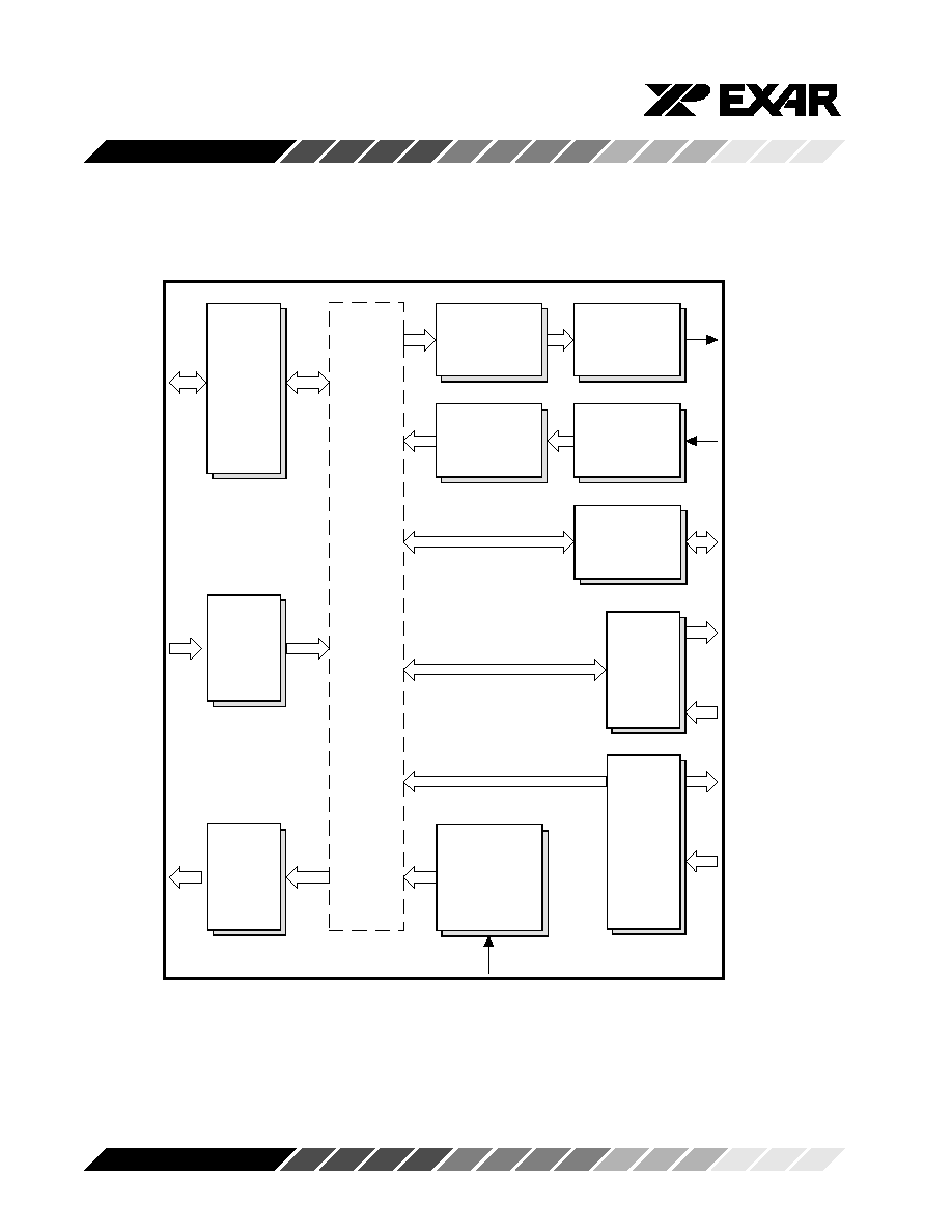
Figure 1, Block Diagram
D0-D7
-IOR
-IOW
-RESET
BIDEN
A0-A2
-CSA
-CSB
-CSP
INT A,B
INTP
-DTR A,B
-RTS A,B
-CTS A,B
-RI A,B
-CD A,B
-DSR A,B
TX A,B
RX A,B
D
a
t
a
bu
s
&
C
o
n
t
r
o
l Lo
g
i
c
Re
g
i
s
t
e
r
S
elect
L
o
gi
c
Modem
Control
Logic
I
n
ter
r
u
p
t
Co
n
t
r
o
l
L
o
gi
c
Transmit
Holding
Registers
Transmit
Shift
Register
Receive
Holding
Registers
Receive
Shift
Register
I
n
ter
C
o
n
n
ect B
u
s
Lin
e
s
&
C
o
n
t
r
o
l
s
i
gn
al
s
Clock
&
Baud Rate
Generator
CL
K
Printer
Data
Ports
PD0-PD7
Printer
Control
Logic
-STROBE
INIT
-AUTOFDX
-SELCTIN
PE, SELECT
-BUSY, -ACK
ERROR

3
ST16C452/452PS
Rev. 3.20
SYMBOL DESCRIPTION
Symbol
Pin
Signal Type
Pin Description
A0
35
I
Address-0 Select Bit - Internal registers address selection.
A1
34
I
Address-1 Select Bit - Internal registers address selection.
A2
33
I
Address-2 Select Bit - Internal registers address selection.
-ACK
68
I
Acknowledge (with internal pull-up) - General purpose input
or line printer acknowledge (active low). a logic 0 from the
printer, indicates successful data transfer to the print buffer.
-AutoFDXT
56
I/O
General purpose I/O (open drain, with internal pull-up) or
automatic line feed (open drain input with internal pull-up).
When this signal is low the printer should automatically line
feed after each line is printed.
BIDEN
1
I
Bi-Direction Enable - PD7-PD0 direction select. A logic 0
sets the parallel port for I/O Select Register Control. A logic
1 sets the parallel port for Control Register Bit-5 Control.
BUSY
66
I
Busy (with internal pull-up) - General purpose input or line
printer busy (active high). can be used as an output from the
printer to indicate printer is not ready to accept data.
CLK
4
I
Clock Input. - An external clock must be connected to this
pin to clock the baud rate generator and internal circuitry
(see Programmable Baud Rate Generator).
-CSA
32
I
Chip Select A - A logic 0 at this pin enables the serial
channel-A UART registers for CPU data transfers.
-CSB
3
I
Chip Select B - A logic 0 at this pin enables the serial
channel-B UART registers for CPU data transfers.
-CSP
38
I
Printer Port Chip Select - (active low). A logic 0 at this pin
enables the parallel printer port registers and/or PD7-PD0
for external CPU data transfers.
D0-D7
14-21
I/O
Data Bus (Bi-directional) - These pins are the eight bit, three
state data bus for transferring information to or from the
controlling CPU. D0 is the least significant bit and the first
data bit in a transmit or receive serial data stream.
4
ST16C452/452PS
Rev. 3.20
SYMBOL DESCRIPTION
Symbol
Pin
Signal Type
Pin Description
-ERROR
63
I
Error, Printer (with internal pull-up) - General purpose input
or line printer error. This pin may be connected to the active
low (logic 0) output of a printer to indicate an error condition.
GND
2,7,54
Pwr
Signal and Power Ground.
27
INIT
57
I/O
Initialize (open drain, with internal pull-up) - General pur-
pose I/O signal. This pin may be connected for initialization
service of a connected line printer. Generally when this
signal is a logic 0, any connected printer will be initialized.
INT A/B
45,60
O
Interrupt output A/B ( three state active high) - These pins
provide individual channel interrupts, INT A-B. INT A-B are
enabled when MCR bit-3 is set to a logic 1, interrupts are
enabled in the interrupt enable register (IER), and when an
interrupt condition exists. Interrupt conditions include: re-
ceiver errors, available receiver buffer data, transmit buffer
empty, or when a modem status flag is detected.
-INTP
59
O
Printer Interrupt, - This pin can be used to signal the
interrupt status of a connected printer. This pin basically
tracks the -ACK input pin, When INTSEL is a logic 0 and
interrupts are enabled by bit-4 in the control register. A
latched mode can be selected by setting INTSEL to a logic
1. In this case the interrupt -INTP is generated normally but
does not return to the inactive state until the trailing edge of
the read cycle (-IOR pin). -INTP is three stated until CON
bit-4 is set to a logic 1.
INTSEL
43
I
Interrupt Select mode - This pin selects the interrupt type for
the printer port (-INTP). When this pin is a logic 0, the
external -ACK signal state is generally followed, minus
some minor propagation delay. Making this pin a logic 1 or
connecting it to VCC will set the interrupt latched mode. In
this case the printer interrupt (-INTP) will not return to a logic
1 until the trailing edge of -IOR (end of the external CPU
read cycle).
-IOR
37
I
Read strobe.- A logic 0 transition on this pin will place the
contents of an Internal register defined by address bits A0-A2

5
ST16C452/452PS
Rev. 3.20
SYMBOL DESCRIPTION
Symbol
Pin
Signal Type
Pin Description
for either UART channels A/B or A0-A1 for the printer port,
onto D0-D7 data bus for a read cycle by an external CPU.
-IOW
36
I
Write strobe.- A logic 0 transition on this pin will transfer the
data on the internal data bus (D0-D7), as defined by either
address bits A0-A2 for UART channels A/B or A0-A1 for the
printer port, into an internal register during a write cycle from
an external CPU.
PD7-PD0
46-53
I/O
Printer Data port (Bi-directional three state) - These pins are
the eight bit, three state data bus for transferring information
to or from an external device (usually a printer). D0 is the
least significant bit. PD7-PD0 are latched during a write
cycle (output mode).
PE
67
I
Paper Empty - General purpose input or line printer paper
empty (Internal pull-up). This pin can be connected to
provide a printer out of paper indication.
RDOUT
44
O
Read Out (active high) - This pin goes to a logic 1 when the
external CPU is reading data from the 452/452PS. This
signal can be used to enable/disable external transceivers
or other logic functions.
-RESET
39
I
Master Reset (active low) - a logic 0 on this pin will reset the
internal registers and all the outputs. The UART transmitter
output and the receiver input will be disabled during reset
time. (See ST16C452/452PS External Reset Conditions for
initialization details.)
N.C.
9,61
Not Used. Should be left open.
SLCT
65
I
Select (with internal pull-up) - General purpose input or line
printer select status. Normally this pin is connected to a
printer output (active low) that indicates the ready status of
a printer, i.e., on-line and/or on-line and ready.
-SLCTIN
58
I/O
Select In (open drain, with internal pull-up) - General
purpose I/O or line printer select. This pin can be read via
Bit-3 in the printer command register, or written via bit-3 in
the printer control register. As this pin is open-drain, it can be
wire-or'd with other outputs. Normally this signal is connected