Exar
Corporation 48720 Kato Road, Fremont CA, 94538
�
(510) 668-7000
�
FAX (510) 668-7017
�
www.exar.com
ST16C654/654D
2.97V TO 5.5V QUAD UART WITH 64-BYTE FIFO
OCTOBER 2003
REV. 5.0.0
GENERAL DESCRIPTION
The ST16C654/654D
1
(654) is an enhanced quad
Universal Asynchronous Receiver and Transmitter
(UART) each with 64 bytes of transmit and receive
FIFOs, transmit and receive FIFO trigger levels,
automatic hardware and software flow control, and
data rates of up to 1.5 Mbps. Each UART has a set of
registers that provide the user with operating status
and control, receiver error indications, and modem
serial interface controls. Selectable interrupt polarity
provides flexibility to meet design requirements. An
internal loopback capability allows onboard
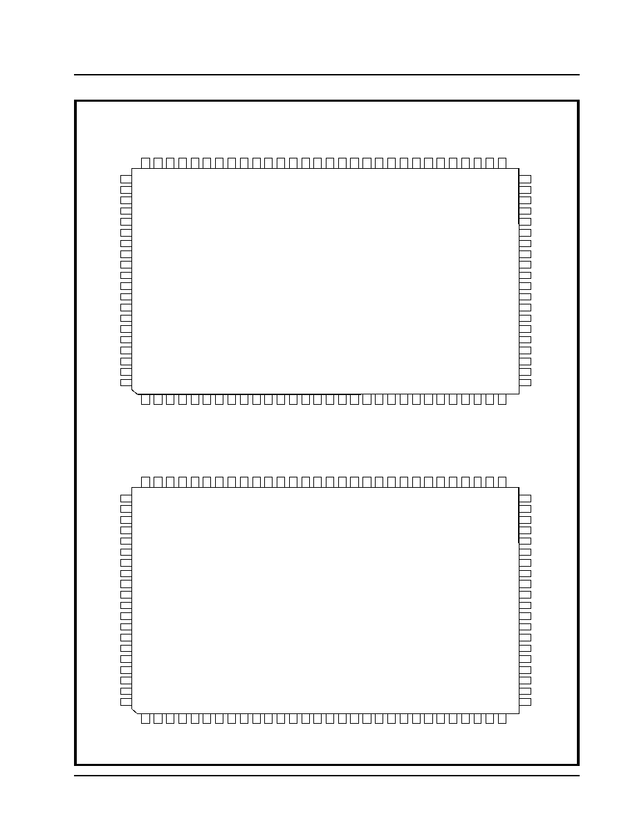
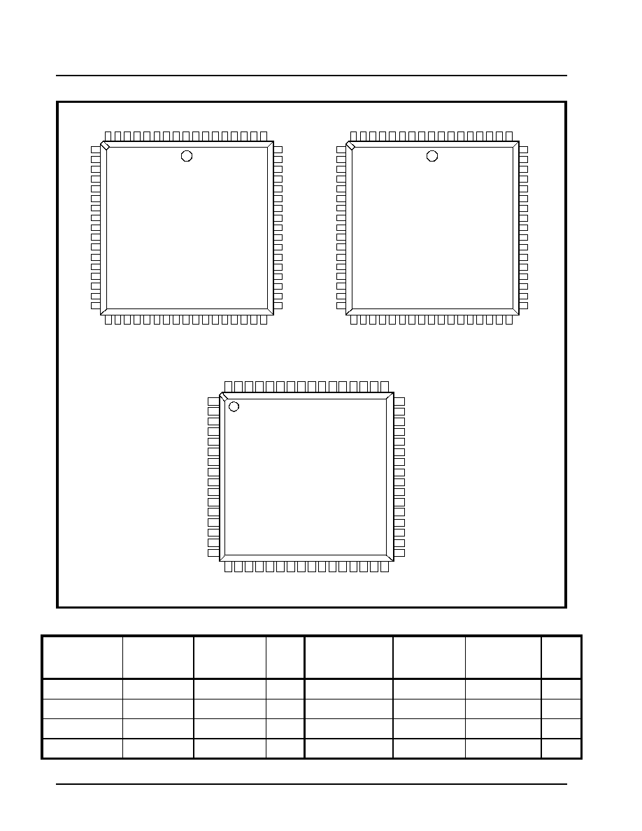
diagnostics. The 654 is available in 64 pin TQFP, 68
pin PLCC and 100 pin QFP packages. The 64 pin
package only offers the 16 mode interface, but the 68
and 100 pin packages offer an additional 68 mode
interface which allows easy integration with Motorola
processors. The ST16C654CQ64 (64 pin) offers
three state interrupt output while the
ST16C654DCQ64 provides continuous interrupt
output. The 100 pin package provides additional
FIFO status outputs (TXRDY# and RXRDY# A-D),
separate infrared transmit data outputs (IRTX A-D)
and channel C external clock input (CHCCLK). The
ST16C654/654D is compatible with the industry
standard ST16C454 and ST16C654/554D.
N
OTE
:
1 Covered by U.S. Patent #5,649,122.
FEATURES
�
Pin-to-pin compatible with ST16C454, ST16C554
and TI's TL16C554AFN and TL16C754BFN
�
Intel or Motorola Data Bus Interface select
�
Four independent UART channels
s
Register Set Compatible to 16C550
s
Data rates of up to 1.5 Mbps
s
64 Byte Transmit FIFO
s
64 Byte Receive FIFO with error tags
s
4 Selectable TX and RX FIFO Trigger Levels
s
Automatic Hardware (RTS/CTS) Flow Control
s
Automatic Software (Xon/Xoff) Flow Control
s
Progammable Xon/Xoff characters
s
Wireless Infrared (IrDA 1.0) Encoder/Decoder
s
Full modem interface
�
2.97V to 5.5V supply operation
�
Sleep Mode (200 uA typical)
�
Crystal oscillator or external clock input
APPLICATIONS
�
Portable Appliances
�
Telecommunication Network Routers
�
Ethernet Network Routers
�
Cellular Data Devices
�
Factory Automation and Process Controls
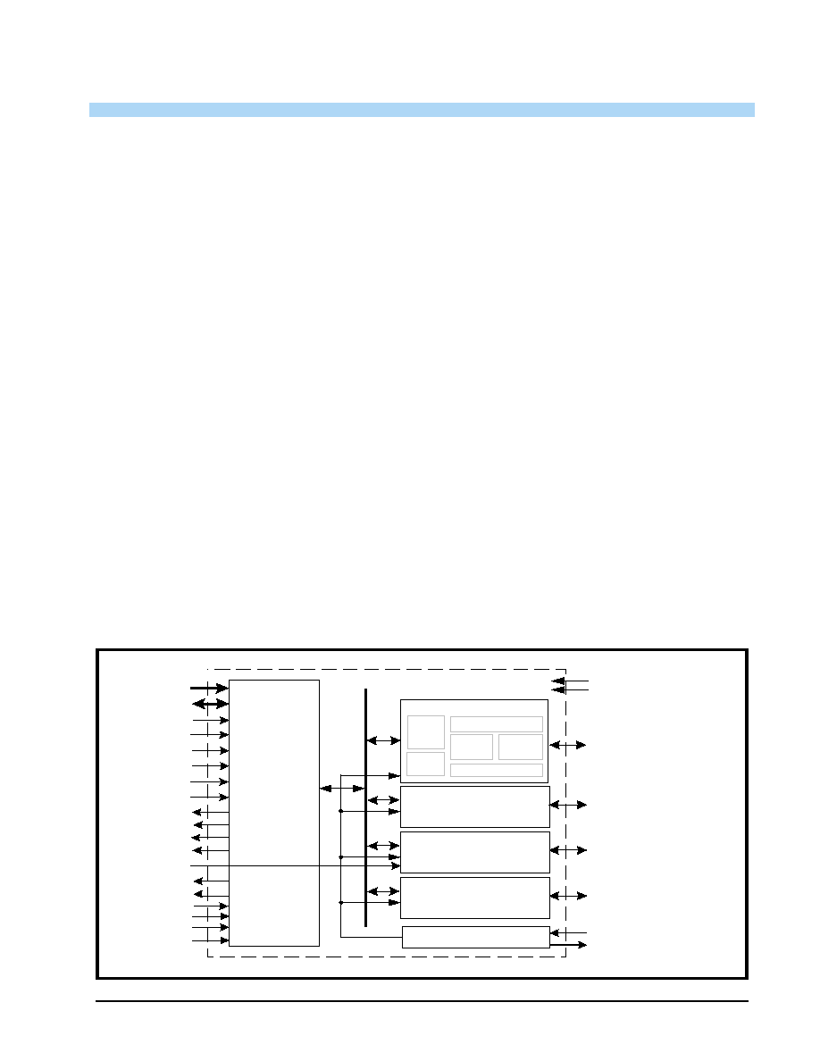
F
IGURE
1. ST16C654 B
LOCK
D
IAGRAM
XTAL1
XTAL2
Crystal Osc/Buffer
Data Bus
Interface
UART Channel A
64 Byte TX FIFO
64 Byte RX FIFO
BRG
IR
ENDEC
TX & RX
UART
Regs
2.97V to 5.5V VCC
GND
654 BLK
TXB, RXB, IRTXB, DTRB#,
DSRB#, RTSB#, CTSB#,
CDB#, RIB#
UART Channel B
(same as Channel A)
A2:A0
D7:D0
CSA#
16/68#
CSB#
INTA
INTB
IOW#
IOR#
Reset
INTSEL
CHCCLK
TXRDY# A-D
RXRDY# A-D
UART Channel C
(same as Channel A)
TXA, RXA, IRTXA, DTRA#,
DSRA#, RTSA#, CTSA#,
CDA#, RIA#
TXC, RXC, IRTXC, DTRC#,
DSRC#, RTSC#, CTSC#,
CDC#, RIC#
UART Channel D
(same as Channel A)
TXD, RXD, IRTXD, DTRD#,
DSRD#, RTSD#, CTSD#,
CDD#, RID#
CSC#
CSD#
INTC
INTD
CLKSEL
ST16C654/654D
2.97V TO 5.5V QUAD UART WITH 64-BYTE FIFO
REV. 5.0.0
4
PIN DESCRIPTIONS
Pin Description
N
AME
64-TQFP
P
IN
#
68-PLCC
P
IN
#
100-QFP
P
IN
#
T
YPE
D
ESCRIPTION
DATA BUS INTERFACE
A2
A1
A0
22
23
24
32
33
34
37
38
39
I
Address data lines [2:0]. These 3 address lines select one of the
internal registers in UART channel A-D during a data bus transac-
tion.
D7
D6
D5
D4
D3
D2
D1
D0
60
59
58
57
56
55
54
53
5
4
3
2
1
68
67
66
95
94
93
92
91
90
89
88
I/O
Data bus lines [7:0] (bidirectional).
IOR#
(VCC)
40
52
66
I
When 16/68# pin is at logic 1, the Intel bus interface is selected and
this input becomes read strobe (active low). The falling edge insti-
gates an internal read cycle and retrieves the data byte from an
internal register pointed by the address lines [A2:A0], puts the data
byte on the data bus to allow the host processor to read it on the ris-
ing edge.
When 16/68# pin is at logic 0, the Motorola bus interface is selected
and this input is not used and should be connected to VCC.
IOW#
(R/W#)
9
18
15
I
When 16/68# pin is at logic 1, it selects Intel bus interface and this
input becomes write strobe (active low). The falling edge instigates
the internal write cycle and the rising edge transfers the data byte on
the data bus to an internal register pointed by the address lines.
When 16/68# pin is at logic 0, the Motorola bus interface is selected
and this input becomes read (logic 1) and write (logic 0) signal.
CSA#
(CS#)
7
16
13
I
When 16/68# pin is at logic 1, this input is chip select A (active low)
to enable channel A in the device.
When 16/68# pin is at logic 0, this input becomes the chip select
(active low) for the Motorola bus interface.
CSB#
(A3)
11
20
17
I
When 16/68# pin is at logic 1, this input is chip select B (active low)
to enable channel B in the device.
When 16/68# pin is at logic 0, this input becomes address line A3
which is used for channel selection in the Motorola bus interface.
CSC#
(A4)
38
50
64
I
When 16/68# pin is at logic 1, this input is chip select C (active low)
to enable channel C in the device.
When 16/68# pin is at logic 0, this input becomes address line A4
which is used for channel selection in the Motorola bus interface.
CSD#
(VCC)
42
54
68
I
When 16/68# pin is at logic 1, this input is chip select D (active low)
to enable channel D in the device.
When 16/68# pin is at logic 0, this input is not used and should be
connected VCC.
ST16C654/654D
2.97V TO 5.5V QUAD UART WITH 64-BYTE FIFO
REV. 5.0.0
5
INTA
(IRQ#)
6
15
12
O
(OD)
When 16/68# pin is at logic 1 for Intel bus interface, this ouput
becomes channel A interrupt output.
7KH RXWSXW VWDWH LV GHILQHG E\
WKH XVHU DQG WKURXJK WKH VRIWZDUH VHWWLQJ RI 0&5>@ ,17$ LV VHW WR
WKH DFWLYH PRGH ZKHQ 0&5>@ LV VHW WR D ORJLF ,17$ LV VHW WR WKH
WKUHH VWDWH PRGH ZKHQ 0&5>@ LV VHW WR D ORJLF GHIDXOW 6HH
0&5>@
When 16/68# pin is at logic 0 for Motorola bus interface, this output
becomes device interrupt output (active low, open drain). An exter-
nal pull-up resistor is required for proper operation.
INTB
INTC
INTD
(N.C.)
12
37
43
21
49
55
18
63
69
O
When 16/68# pin is at logic 1 for Intel bus interface, these ouputs
become the interrupt outputs for channels B, C, and D.
7KH RXWSXW
VWDWH LV GHILQHG E\ WKH XVHU WKURXJK WKH VRIWZDUH VHWWLQJ RI 0&5>@
7KH LQWHUUXSW RXWSXWV DUH VHW WR WKH DFWLYH PRGH ZKHQ 0&5>@ LV VHW
WR D ORJLF DQG DUH VHW WR WKH WKUHH VWDWH PRGH ZKHQ 0&5>@ LV VHW
WR D ORJLF GHIDXOW 6HH 0&5>@
When 16/68# pin is at logic 0 for Motorola bus interface, these out-
puts are unused and will stay at logic zero level. Leave these out-
puts unconnected.
INTSEL
-
65
87
I
Interrupt Select (active high, input with internal pull-down).
When 16/68# pin is at logic 1 for Intel bus interface, this pin can be
used in conjunction with MCR bit-3 to enable or disable the INT A-D
pins or override MCR bit-3 and enable the interrupt outputs. Inter-
rupt outputs are enabled continuously by making this pin a logic 1.
Making this pin a logic 0 allows MCR bit-3 to enable and disable the
interrupt output pins. In this mode, MCR bit-3 is set to a logic 1 to
enable the continuous output. See MCR bit-3 description for full
detail. This pin must be at logic 0 in the Motorola bus interface
mode. Due to pin limitations on 64 pin packages, this pin is not
available. To cover this limitation, two 64 pin TQFP packages ver-
sions are offered. This pin is bonded to VCC internally in the
ST16C654D so the INT outputs operate in the continuous interrupt
mode. This pin is bonded to GND internally in the ST16C654 and
therefore requires setting MCR bit-3 for enabling the interrupt output
pins.
TXRDYA#
TXRDYB#
TXRDYC#
TXRDYD#
-
-
-
-
-
-
-
-
5
25
56
81
O
UART channels A-D Transmitter Ready (active low). The outputs
provide the TX FIFO/THR status for transmit channels A-D. See
Table 5
. If these outputs are unused, leave them unconnected.
RXRDYA#
RXRDYB#
RXRDYC#
RXRDYD#
-
-
-
-
-
-
-
-
100
31
50
82
O
UART channels A-D Receiver Ready (active low). This output pro-
vides the RX FIFO/RHR status for receive channels A-D. See
Table 5
. If these outputs are unused, leave them unconnected.
TXRDY#
-
39
45
O
Transmitter Ready (active low). This output is a logically ANDed
status of TXRDY# A-D. See
Table 5
. If this output is unused, leave
it unconnected.
RXRDY#
-
38
44
O
Receiver Ready (active low). This output is a logically ANDed status
of RXRDY# A-D. See
Table 5
. If this output is unused, leave it
unconnected.
Pin Description
N
AME
64-TQFP
P
IN
#
68-PLCC
P
IN
#
100-QFP
P
IN
#
T
YPE
D
ESCRIPTION