ST26C32
...the analog plus company
TM
QUAD RS-422, RS-423 CMOS
Differential Line Receiver
Rev. 1.01
E
1991
EXAR Corporation, 48720 Kato Road, Fremont, CA 94538
z
(510) 668-7000
z
FAX (510) 668-7017
1
June 1997≠3
FEATURES
D
Pin-to-Pin Compatible with National DS26C32C
D
Low Power CMOS Design
D
Three-State Outputs with Enable Pin
D
Meets the EIA RS-422 Requirements
D
Low Propagation Delays
D
High Speed
GENERAL DESCRIPTION
The ST26C32 is a CMOS quad differential line receiver
designed to meet the standard RS-422, RS-423
requirements. The ST26C32 has an input sensitivity of
200mv over the common mode input voltage range of
±
7V. To improve noise margin and output stability for slow
changing input signal, special hysteresis is built in the
ST26C32 circuit.
The ST26C32 is a high speed line receiver designed to
operate with MFM / RLL controllers and hard disk drives
as well as RS-422, and RS-423 differential applications.
ST26C32 provides TTL compatible outputs to interface
with standard 74LS and CMOS design environments.
ST26C32 is suitable for low power 5V operation.
ORDERING INFORMATION
Part No.
Package
Operating
Temperature Range
ST26C32CP16
16 Lead 300 Mil PDIP
0
∞
C to +70
∞
C
ST26C32CF16
16 Lead 150 Mil JEDEC SOIC
0
∞
C to +70
∞
C
ST26C32IP16
16 Lead 300 Mil PDIP
-40
∞
C to +85
∞
C
ST26C32IF16
16 Lead 150 Mil JEDEC SOIC
-40
∞
C to +85
∞
C
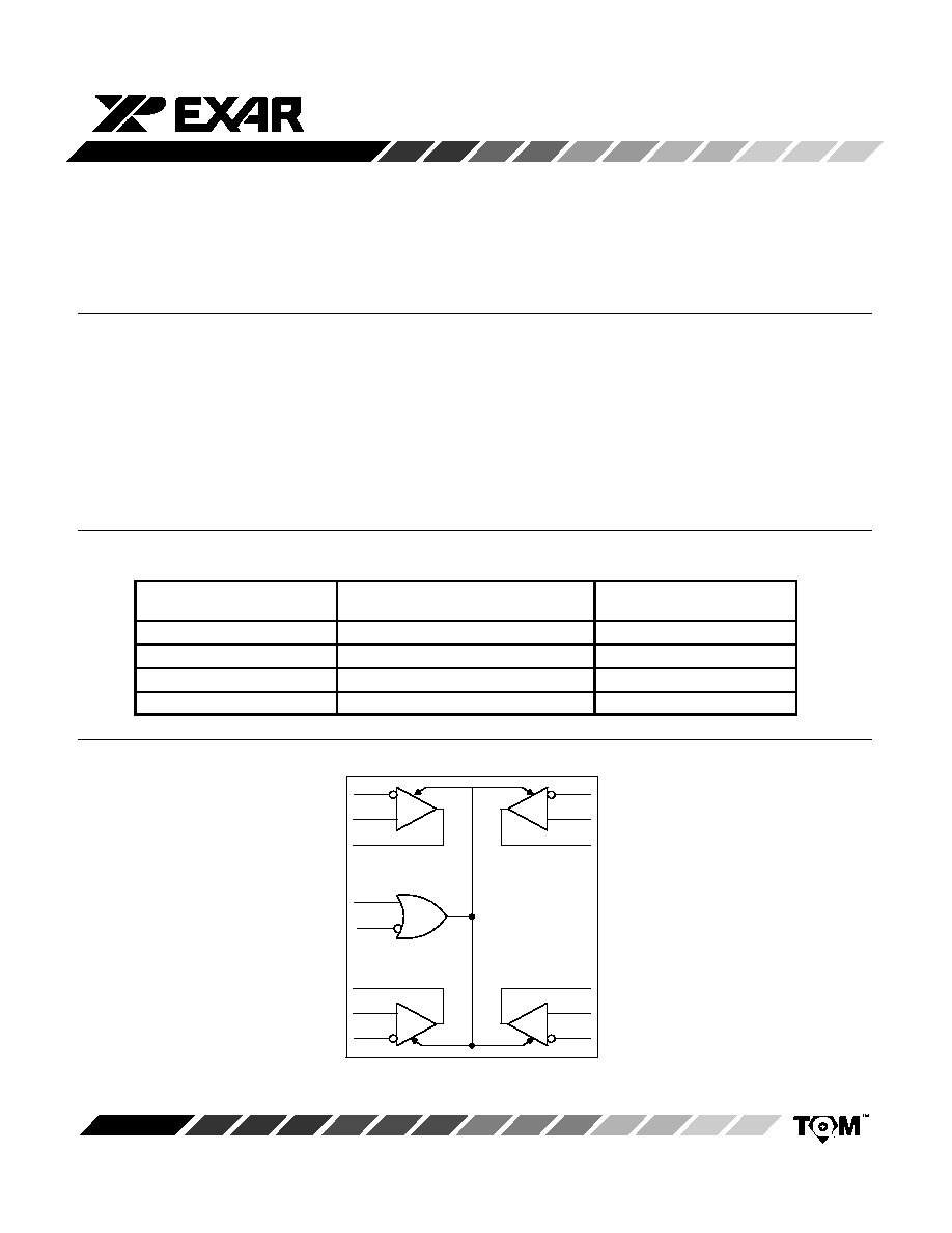
Figure 1. Block Diagram
INPUT D-
INPUT D+
OUTPUT D
-ENABLE
OUTPUT C
INPUT C+
INPUT C-
INPUT A-
INPUT A+
OUTPUT A
ENABLE
INPUT B-
INPUT B+
OUTPUT B
ST26C32
2
Rev. 1.01
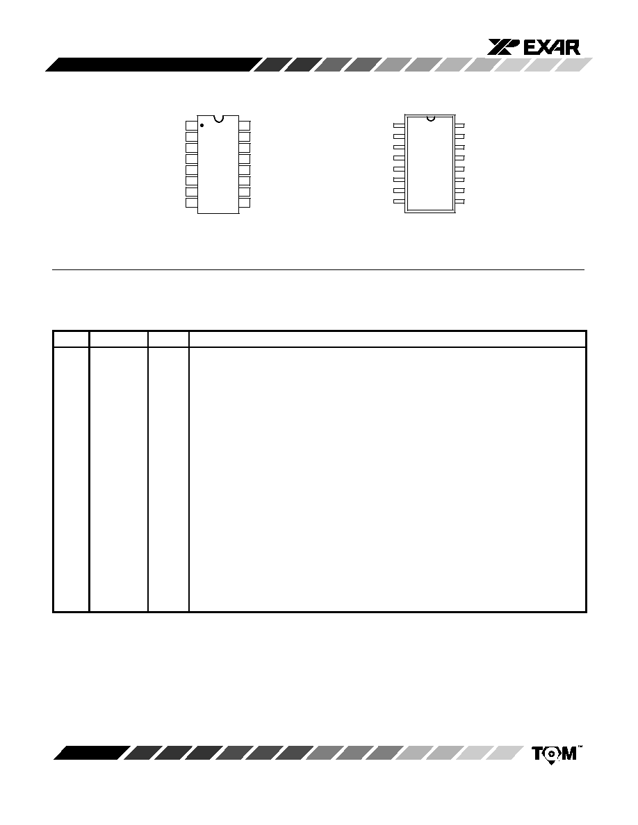
PIN CONFIGURATION
16 Lead PDIP (0.300")
V
CC
INPUT D
OUTPUT D+
OUTPUT D-
-ENABLE
OUTPUT C-
OUTPUT C+
INPUT C
INPUT A
OUTPUT A+
OUTPUT A-
ENABLE
OUTPUT B-
OUTPUT B+
INPUT B
GND
1
2
3
4
5
6
7
8
16
15
14
13
12
11
10
9
16 Lead SOIC (Jedec, 0.150")
16
1
9
8
2
3
4
5
6
7
15
14
13
12
11
10
V
CC
INPUT D
OUTPUT D+
OUTPUT D-
-ENABLE
OUTPUT C-
OUTPUT C+
INPUT C
INPUT A
OUTPUT A+
OUTPUT A-
ENABLE
OUTPUT B-
OUTPUT B+
INPUT B
GND
PIN DESCRIPTION
Pin #
Symbol
Type
Description
1
INPUT A-
I
Receiver A differential inverting input pin.
2
INPUT A+
I
Receiver A differential non-inverting input pin.
3
OUTPUT A
O
Receiver A output pin.
4
ENABLE
I
Gate control (active high). This pin is one of the two control pins which enables or disables all
four receivers.
5
OUTPUT B
O
Receiver B output pin.
6
INPUT B+
I
Receiver B differential non-inverting input pin.
7
INPUT B-
I
Receiver B differential inverting input pin.
8
GND
O
Signal and power ground.
9
INPUT C-
I
Receiver C differential inverting input pin.
10
INPUT C+
I
Receiver C differential non-inverting input pin.
11
OUTPUT C
O
Receiver C output pin.
12
-ENABLE
I
Gate control (active low). See ENABLE description
13
OUTPUT D
O
Receiver D output pin.
14
INPUT D+
I
Receiver D differential non-inverting input pin.
15
INPUT D-
I
Receiver D differential inverting input pin.
16
V
CC
I
Power supply pin.
ST26C32
3
Rev. 1.01
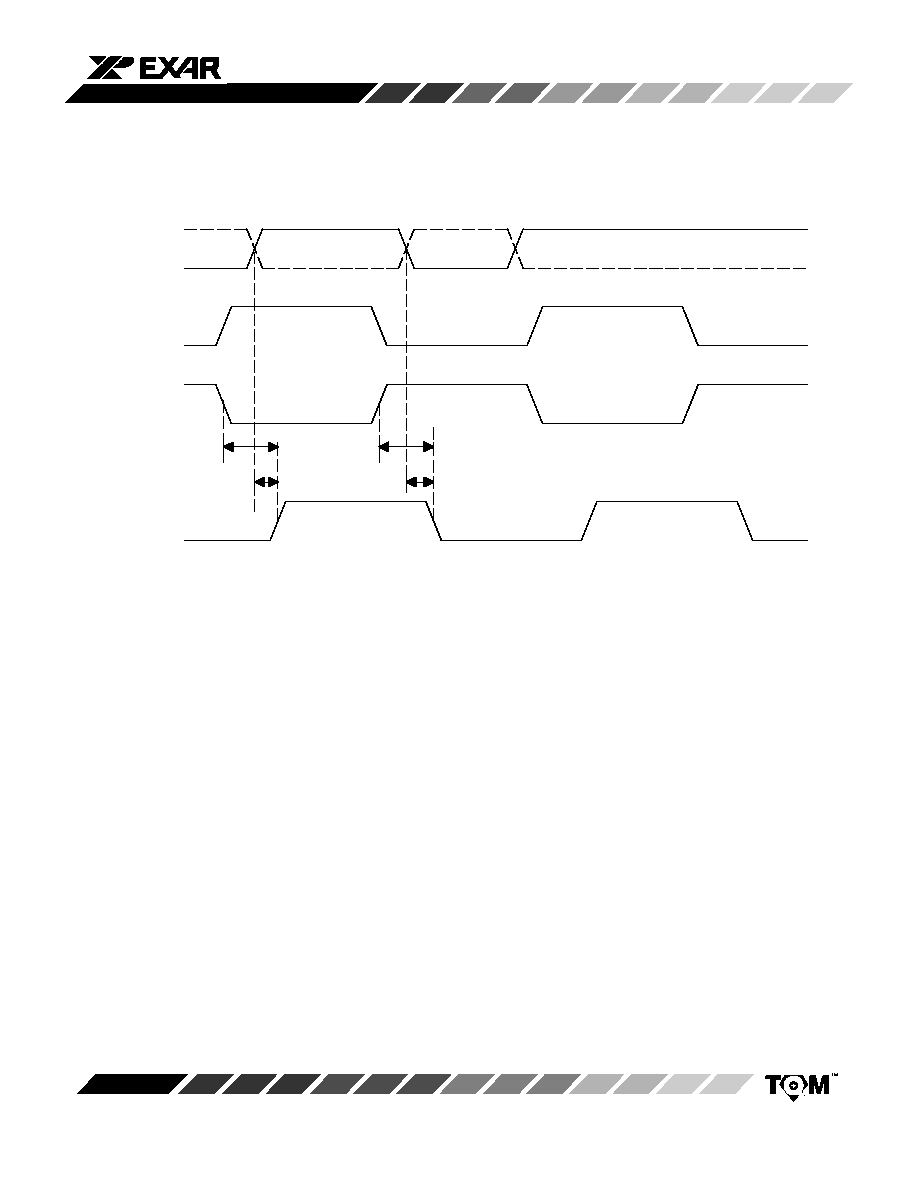
AC ELECTRICAL CHARACTERISTICS
Test Conditions: T
A
= -40
∞
C - +85
∞
C, V
CC
= 5.0V + 10% unless otherwise specified.
Symbol
Parameter
Min.
Typ.
Max.
Unit
Conditions
T
1
Propagation Delay, Input to
Output
8
10
ns
S1=V
CC
T
2
Propagation Delay, Input to
Output
18
20
ns
S1=GND
T
3
Output Enable Time
18
20
ns
V
DIF
=2.5V
T
4
Output Disable Time
18
20
ns
V
DIF
=2.5V
DC ELECTRICAL CHARACTERISTICS
Test Conditions: T
A
= -40
∞
C - +85
∞
C, V
CC
= 5.0V + 10% unless otherwise specified.
Symbol
Parameter
Min.
Typ.
Max.
Unit
Conditions
V
IH
Enable High Level
2.0
V
V
IL
Enable Low Level
0.8
V
V
OH
Output High Level
3.8
4.2
V
I
OH
= -6mA
V
OL
Output Low Level
0.4
V
I
OH
= 6mA
V
ID
Differential Input Level
-0.2
0.2
V
-7V < V
CM
< +7V
V
H
Input Hysteresis
50
mV
I
IN
Input Current
+1.0
m
A
I
CC
Operating Current
12
mA
V
DIF
=+1V
I
OZ
Three-State Output Leakage
+1.0
+5.0
m
A
V
OUT
=V
CC
or GND
I
EN
Enable Input Current
+1.0
m
A
V
IN
=V
CC
or GND
V
R
Input Resistance
5
15
K
W
-7V < V
CM
< +7V
Specifications are subject to change without notice
ABSOLUTE MAXIMUM RATINGS
Supply Range
7V
. . . . . . . . . . . . . . . . . . . . . . . . . . . . . . .
Voltage at Any Pin
GND-0.3V to V
CC
+ 0.3V
. . . . . . . .
Operating Temperature
≠40
∞
C to +85
∞
C
. . . . . . . . . . .
Storage Temperature
-60
∞
C to +160
∞
C
. . . . . . . . . . . .
Package Dissipation
500mW
. . . . . . . . . . . . . . . . . . . . .
ST26C32
4
Rev. 1.01
Enable
-Enable
Input
Differential
Non-Inverting
Output
Differential
Inverting
Output
L
H
Z
X
X
H
L
L
L
H
H
L
H
H
L
Notes
X = Don't care
Z = Three-State (high impedance)
Table 1. Functional Table
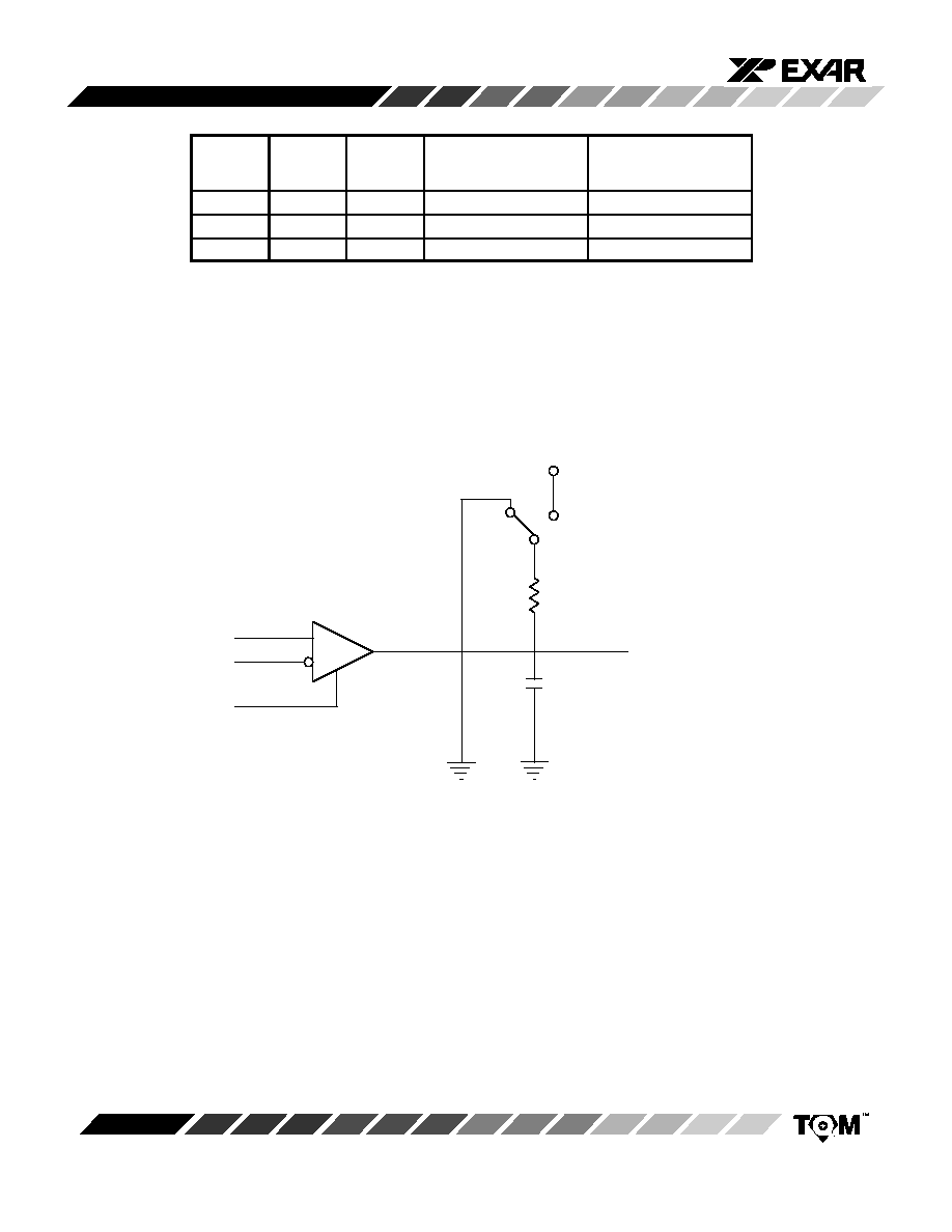
Figure 2. Test Condition
INPUT A
-INPUT A
-ENABLE
Receiver
U1
V
CC
S1
R1
10K
C1
50pF
OUTPUT A
ST26C32
5
Rev. 1.01
ENABLE
-ENABLE
OUTPUT X
INPUT X+
INPUT X-
T
3
T
4
T
2
T
1
Figure 3. Differential Line Receiver Timing