ST49C107A-04
...the analog plus company
TM
Preprogrammed CPU Mother Board
Frequency Generator
Preliminary
Rev. P2.00
E
1996
EXAR Corporation, 48720 Kato Road, Fremont, CA 94538
z
(510) 668-7000
z
FAX (510) 668-7017
1
June 1997-3
FEATURES
D
Provides Reference Clock And Synthesized Clock
D
5 to 32 MHz Input Reference Frequency
D
Pin-to-Pin Compatible to Avasem AV9107
D
Programmable Analog Phase Locked Loop
D
Low Power Single 5V CMOS Technology
D
Up to 16 Frequencies Stored Internally
D
8/14 pin DIP or SOIC Package
GENERAL DESCRIPTION
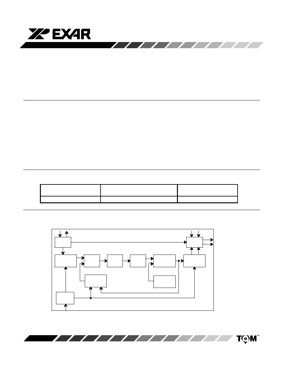
The ST49C107A-04 is a mask programmable monolithic
analog CMOS device designed to generate two
simultaneous clocks. The output frequency can vary from
2 to 130MHz, with up to 16 single selectable
preprogrammed frequencies stored in internal ROM.
The ST49C107A-04 is designed to replace existing CPU
mother board clocks generated from individual oscillators
in order to reduce board space and number of oscillators.
To provide high speed and low jitter clock, the parts utilize
a high speed analog CMOS phase locked loop using
14.318 MHz system clock as the reference clock (note
that reference clock can be changed to generate optional
frequencies from a standard programmed device). The
programmed clock outputs are selectable via four
address lines.
ORDERING INFORMATION
Part No.
Package
Operating
Temperature Range
ST49C107ACF14-04
14 Lead 150 Mil JEDEC SOIC
0
�
C to 70
�
C
BLOCK DIAGRAM
Oscillator
Circuit
Programmable
Counter
B
Phase
Detector
Charge
Pump
Loop
Filter
Voltage
Controlled
Oscillator
Programmable
Counter
C
Voltage
Reference
Circuit
Programmable
Counter
A
Output
Buffer
1X-CLOCK
XTAL
XTAL
B=5....128
A=5....128
C = 1, 2, 4
Rom Table
Select
Logic
A0-A3
OE1 OE2
2X-CLOCK
Figure 1. Block Diagram
ST49C107A-04
Preliminary
2
Rev. P2.00
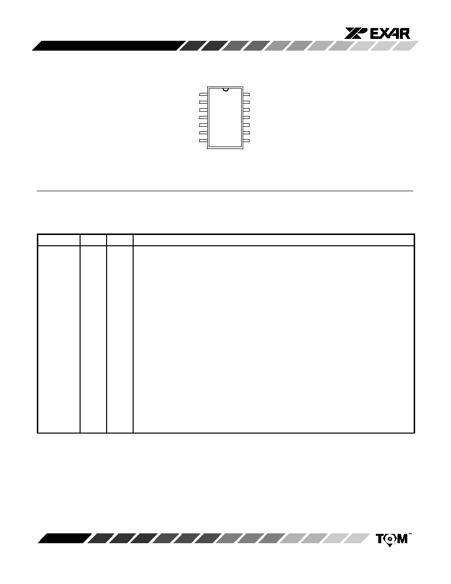
PIN CONFIGURATION
14 Lead SOIC (Jedec, 0.150")
14
1
2
3
4
5
6
7
13
12
11
10
9
8
A0
1XCLK
V
CC
2XCLK
OE2
OE1
XTAL2
A1
A2
A3
AGND
DGND
PD*
XTAL1
PIN DESCRIPTION
Symbol
Pin #
Type
Description
A1
1
I
Frequency Select Address Input 2
1
.
A2
2
I
Frequency Select Address Input 3
1
.
A3
3
I
Frequency Select Address Input 4
1
.
AGND
4
O
Analog Ground.
DGND
5
O
Digital Ground.
PD
6
I
Power-down (Active Low). Shuts off chip when low
1
.
XTAL1
7
I
Crystal Or External Clock Input. A crystal can be connected to this pin and XTAL2 pin to
generate internal phase locked loop reference clock. For external 14.318 MHz clock, XTAL2
is left open or used as buffered clock output.
XTAL2
8
O
Crystal Output.
OE1
9
I
1X-CLOCK Output Enable (Active High). 1X-CLOCK output is three stated when this pin is
low
1
.
OE2
10
I
2X-CLOCK Output Enable (Active High). 2X-CLOCK output is three stated when this pin is
low
1
.
2XCLK
11
O
Programmed Output Clock.
V
CC
12
I
Positive Supply Voltage. Single +5 volts.
1XCLK
13
O
2X-CLOCK Divide-by-two Output.
A0
14
I
Frequency Select Address Input 1
1
.
Notes
1
Have internal pull-up resistors on inputs.
ST49C107A-04
Preliminary
3
Rev. P2.00
DC ELECTRICAL CHARACTERISTICS
Test Conditions: T
A
= 0
�
C to +70
�
C, V
CC
= 5.0V
10% Unless Otherwise Specified
Symbol
Parameter
Min.
Typ.
Max.
Unit
Conditions
V
IL
Input Low Level
0.8
V
V
IH
Input High Level
2.0
V
V
OL
Output Low Level
0.4
V
I
OL
= 8.0mA
V
OH
Output High Level
2.4
V
I
OH
= 8.0mA
I
IL
Input Low Current
-10
�
A
Except Crystal Input
I
IH
Input High Current
1
�
A
V
IN
=V
CC
I
CC
Operating Current
45
55
mA
No Load. CLOCK=100MHz
I
SB
Standby Current
25
�
A
No Load
R
IN
Input Pull-up Resistance
500
900
1300
k
DC ELECTRICAL CHARACTERISTICS
Test Conditions: T
A
= 0
�
C to +70
�
C, V
CC
= 5.0V
10% Unless Otherwise Specified
Symbol
Parameter
Min.
Typ.
Max.
Unit
Conditions
T
1
1X, 2X-CLOCK Rise Time
1
2
ns
CL=20pF 0.8V - 2.0V
T
2
1X, 2X-CLOCK Fall Time
1
2
ns
CL=20pF 2.0V - 0.8V
T
4
Duty Cycle
40
50
60
%
1.4V Switch Point
T
5
Duty Cycle
45
50
55
%
V
CC
/2 Switch Point
T
3
Jitter 1 Sigma
0.5
2
%
T
3
Jitter Absolute
3
5
%
T
Input Frequency
2
32
MHz
T
7
Buffered Clock Rise Time
20
ns
T
8
Buffered Clock Fall Time
20
ns
Specifications are subject to change without notice
ABSOLUTE MAXIMUM RATINGS
Supply Range
7 Volts
. . . . . . . . . . . . . . . . . . . . . . . . . . .
Voltage at Any Pin
GND-0.3V to V
CC
+0.3V
. . . . . . . . .
Operating Temperature
0
�
C to +70
�
C
. . . . . . . . . . . . .
Storage Temperature
-40
�
C to +150
�
C
. . . . . . . . . . . .
Package Dissipation
500 mW
. . . . . . . . . . . . . . . . . . . . .
ST49C107A-04
Preliminary
4
Rev. P2.00
EXTERNAL CLOCK CONNECTION
To minimize the noise pickup, it is recommended to
connect 0.047 (F capacitor to XTAL1, and keep the lead
length of the capacitor to XTAL1 to a minimum to reduce
noise susceptibility.
FREQUENCY SELECT CALCULATION
The ST49C107A-04 contains an analog phase locked
loop circuit with digital closed loop dividers and a final
output multiplexer to achieve the desired dividing ratios
for the clock output.
The accuracy of the frequencies produced by the
ST49C107A-04 depends on the input frequency and
divider ratios. The formula for calculating the exact output
frequency is as follows:
CLKOUT = CLKIN * Factor
For proper output frequency, the ST49C107A-04 can
accept a reference frequency from 5 - 32MHz with max
output frequency of 130MHz (2X � clock).
CLOCK OUTPUT TABLE FOR ST49C107A-04 (using
14.318 MHz input. All frequencies in MHz).
A3
A2
A1
A0
Factor
2X-
CLOCK
CLOCK
0
0
0
0
95/17
80.02
40.01
0
0
0
1
107/23
66.62
33.31
0
0
1
0
35/10
50.11
25.06
0
0
1
1
95/34
40.01
20.00
0
1
0
0
56/8
100.23
50.11
0
1
0
1
107/46
33.31
16.66
0
1
1
0
38/17
32.01
16.00
0
1
1
1
35/20
25.06
12.47
1
0
0
0
76/17
64.02
32.01
1
0
0
1
2
2X-Input
1X-Input
1
0
1
0
3
3X-Input
1.5X-Input
1
0
1
1
8
8X-Input
4X-Input
1
1
0
0
1/2
0.5X-Input
0.25X-Input
1
1
0
1
1/4
0.25X-
Input
0.125X-
Input
1
1
1
0
109/13
120.00
60.00
1
1
1
1
118/13
129.96
64.98
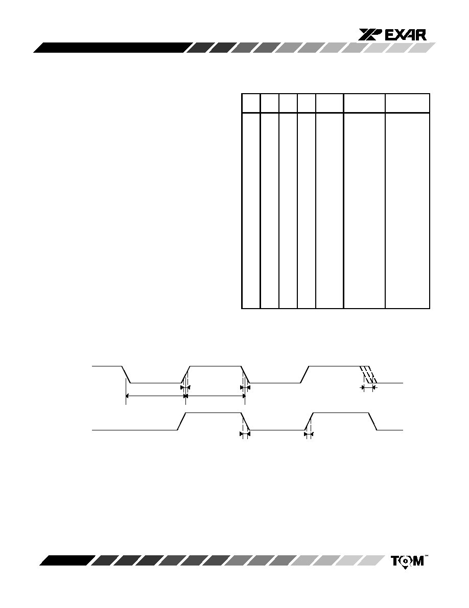
Figure 2. Timing Diagram
T5
T1
T4
CLOCK
T2
2X�CLOCK
1X�CLOCK
T8
T7
BCLK
T3
ST49C107A-04
Preliminary
5
Rev. P2.00
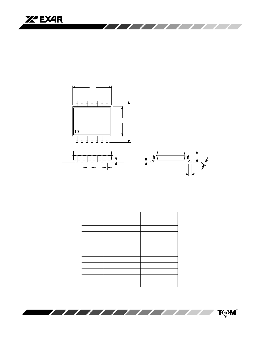
SYMBOL
MIN
MAX
MIN
MAX
A
0.053
0.069
1.35
1.75
A
1
0.004
0.010
0.10
0.25
B
0.013
0.020
0.33
0.51
C
0.007
0.010
0.19
0.25
D
0.337
0.344
8.55
8.75
E
0.150
0.157
3.80
4.00
e
0.050 BSC
1.27 BSC
H
0.228
0.244
5.80
6.20
L
0.016
0.050
0.40
1.27
0
�
8
�
0
�
8
�
INCHES
MILLIMETERS
14 LEAD SMALL OUTLINE
(150 MIL JEDEC SOIC)
Rev. 1.00
e
14
8
7
D
E
H
B
A
L
C
A
1
Seating
Plane
Note: The control dimension is the millimeter column
1

ST49C107A-04
Preliminary
6
Rev. P2.00
Notes

ST49C107A-04
Preliminary
7
Rev. P2.00
Notes

ST49C107A-04
Preliminary
8
Rev. P2.00
NOTICE
EXAR Corporation reserves the right to make changes to the products contained in this publication in order to im-
prove design, performance or reliability. EXAR Corporation assumes no responsibility for the use of any circuits de-
scribed herein, conveys no license under any patent or other right, and makes no representation that the circuits are
free of patent infringement. Charts and schedules contained here in are only for illustration purposes and may vary
depending upon a user's specific application. While the information in this publication has been carefully checked;
no responsibility, however, is assumed for inaccuracies.
EXAR Corporation does not recommend the use of any of its products in life support applications where the failure or
malfunction of the product can reasonably be expected to cause failure of the life support system or to significantly
affect its safety or effectiveness. Products are not authorized for use in such applications unless EXAR Corporation
receives, in writing, assurances to its satisfaction that: (a) the risk of injury or damage has been minimized; (b) the
user assumes all such risks; (c) potential liability of EXAR Corporation is adequately protected under the circum-
stances.
Copyright 1996 EXAR Corporation
Datasheet June 1997
Reproduction, in part or whole, without the prior written consent of EXAR Corporation is prohibited.