EXAR Corporation, 48720 Kato Road, Fremont, CA 94538
∑
(510) 668-7000
∑
FAX (510) 668-7017
Rev. 1.20
XR16C850
UART with 128-byte FIFO's
FIFO Counters and Half-duplex Control
June 1999-1
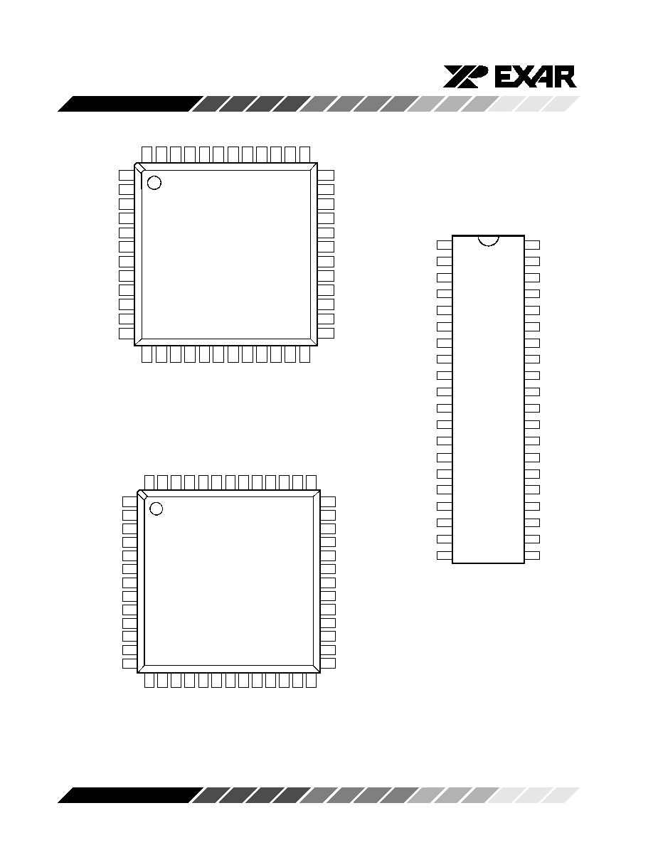
PLCC Package
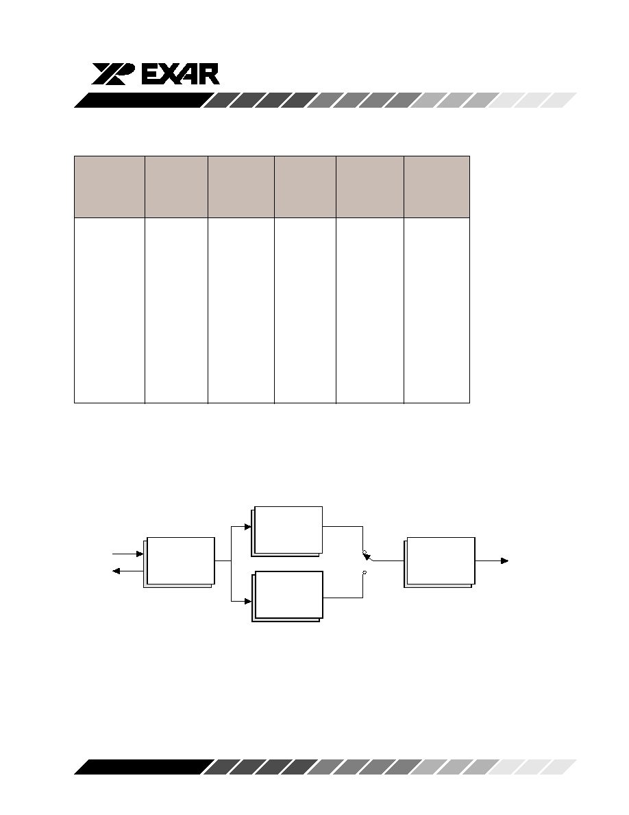
Part Number
Pins
Package Operating Temperature
XR16C850IP
40
PDIP
-40∞ C to + 85∞ C
XR16C850IJ
44
PLCC
-40∞ C to + 85∞ C
XR16C850IM
48
TQFP
-40∞ C to + 85∞ C
XR16C850IQ
52
QFP
-40∞ C to + 85∞ C
6
5
4
3
2
1
44
43
42
41
40
7
8
9
10
11
12
13
14
15
16
17
39
38
37
36
35
34
33
32
31
30
29
18
19
20
21
22
23
24
25
26
27
28
D5
D6
D7
RCLK
RX
N.C.
TX
CS0
CS1
-CS2
-BAUDOUT
RESET
-OP1
-DTR
-RTS
-OP2
N.C.
INT
-RXRDY
A0
A1
A2
D4
D3
D2
D1
D0
N.
C.
VC
C
-R
I
-C
D
-D
S
R
-C
T
S
XT
AL
1
XT
AL
2
-I
O
W
IO
W
GN
D
N.
C.
-I
O
R
IO
R
-
DDI
S
-T
X
R
DY
-A
S
XR16C850CJ
"STD" MODE
CONNECTION
6
5
4
3
2
1
44
43
42
41
40
7
8
9
10
11
12
13
14
15
16
17
39
38
37
36
35
34
33
32
31
30
29
18
19
20
21
22
23
24
25
26
27
28
D5
D6
D7
S2
RX
A4
TX
A5
A6
A7
-LPT1
RESET
-OP1
-DTR
-RTS
S3
GND
IRQA
IRQB
A0
A1
A2
D4
D3
D2
D1
D0
A9
VC
C
-R
I
-C
D
-D
S
R
-C
T
S
XT
AL
1
XT
AL
2
-
IOW
A8
GN
D
S1
-
IOR
A3
-L
PT
2
IR
QC
-AEN
XR16C850CJ
"PC" MODE
CONNECTION
GENERAL DESCRIPTION
The XR16C850
*1
(850) is a universal asynchronous
receiver and transmitter (UART) and is pin compatible
with the ST16C550,ST16C650A, and TI's TL16C750
UART. The 850 is an enhanced UART with 128 byte
FIFOs, automatic hardware/software flow control, and
data rates up to 1.5Mbps. It includes transmit/receive
FIFO counters to increase data loading and unloading
throughput. Onboard status registers provide error indi-
cations and operational status. Modem interface con-
trol is included and can be optionally configured to
operate with the Infrared (IrDA) encoder/decoder. Inter-
nal loopback allows onboard diagnostics. The 850 is
available in 40-pin PDIP, 44-pin PLCC, 48-pin TQFP,
and 52-pin QFP packages. The 44, 48, and 52 pin
versions provide both the standard (STD) mode or PC
mode. The STD mode is compatible with the ST16C450,
ST16C550, ST16C650A and TL16C750 while the PC
mode supports standard PC COM port connections.
The 40 PDIP pin package does not offer the PC mode.
FEATURES
∑
Pin to pin compatible to ST16C550, ST16C650A and
TL16C750
∑
Transmit/receive FIFO counters
∑
128 bytes of Transmit/Receive FIFO
∑
RS-485 half duplex direction control
∑
Automatic software/hardware flow control
∑
Programmable, selectable transmit/receive trigger
levels
∑
Infrared transmitter and receiver encoder/decoder
∑
Up to 1.5Mbps data rate
∑
Sleep mode (100
µ
A standby)
∑
Small 7x7mm TQFP
∑
+5 or 3.3 Volts operation
∑
Windows
2
drivers available
ORDERING INFORMATION
Part Number
Pins
Package Operating Temperature
XR16C850CP
40
PDIP
0∞ C to + 70∞ C
XR16C850CJ
44
PLCC
0∞ C to + 70∞ C
XR16C850CM 48
TQFP
0∞ C to + 70∞ C
XR16C850CQ 52
QFP
0∞ C to + 70∞ C
Note *1: Covered by U.S. patent # 5,649,122 and patent pending.
Note *2: Windows is a trademark of Microsoft Corporation.
XR16C850
2
Rev. 1.20
48
47
46
45
44
43
42
41
40
39
38
37
1
2
3
4
5
6
7
8
9
10
11
12
36
35
34
33
32
31
30
29
28
27
26
25
13
14
15
16
17
18
19
20
21
22
23
24
D11
D5
D6
D7
S2 / RCLK
A4
RX
TX
A5 / CS0
A6 / CS1
A7 / -CS2
-LPT1 / -BAUDOUT
C
L
KSE
L
XT
AL
1
XT
AL
2
-
IOW
A
8
/
IOW
GN
D
-
IOR
A
3
/
IOR
S1
D
12/
-
L
P
T
2
/
-
D
DI
S
IR
QC
/ -
T
X
R
D
Y
-AE
N
/
-A
S
SEL
RESET
-OP1/RS485
-DTR
-RTS
-OP2 / S3
INT / IRQA
-RXRDY / IRQB
A0
A1
A2
BUS 8/16
D1
0
D4
D3
D2
D1
D0
VC
C
-R
I
-C
D
-D
SR
-C
T
S
A9
XR16C850CM
Figure 1. PACKAGE DESCRIPTION, 16C850
52
51
50
49
48
47
46
45
44
43
42
41
40
1
2
3
4
5
6
7
8
9
1 0
1 1
1 2
1 3
3 9
3 8
3 7
3 6
3 5
3 4
3 3
3 2
3 1
3 0
2 9
2 8
2 7
14
15
16
17
18
19
20
21
22
23
24
25
26
D 1 1
D 5
D 6
D 7
S2 / RCLK
A 4
R X
T X
A5 / CS0
A6 / CS1
A7 / -CS2
- L P T 1 / - B A U D O U T
T C
CLKSEL
XTAL1
XTAL2
-IOW
A8 / IOW
GND
-DMA
-IOR
A3 / IOR
S1
D12/-LPT2 /- DDIS
IRQC / -TXRDY
-AEN /- AS
S E L
R E S E T
- O P 1 / R S 4 8 5
- D T R
- R T S
-OP2 / S3
INT / IRQA
- R X R D Y * / I R Q B / D R Q
A 0
A 1
A 2
BUS 8/16
CLK 8/16
D10
D4
D3
D2
D1
D0
-DACK
VCC
-RI
-CD
-DSR
-CTS
A9
X R 1 6 C 8 5 0 C Q
1
2
3
4
5
6
7
8
9
1 0
1 1
1 2
1 3
1 4
1 5
1 6
1 7
1 8
1 9
2 0
4 0
3 9
3 8
3 7
3 6
3 5
3 4
3 3
3 2
3 1
3 0
2 9
2 8
2 7
2 6
2 5
2 4
2 3
2 2
2 1
D 0
D 1
D 2
D 3
D 4
D 5
D 6
D 7
R C L K
R X
T X
C S 0
C S 1
- C S 2
- B A U D O U T
X T A L 1
X T A L 2
- I O W
I O W
G N D
V C C
-RI
- C D
- D S R
- C T S
R E S E T
- O P 1
- D T R
- R T S
- O P 2
I N T
- R X R D Y
A 0
A 1
A 2
- A S
- T X R D Y
- D D I S
I O R
- I O R
XR16C850CP
XR16C850
3
Rev. 1.20
D0-D7
-IOR,IOR
-IOW,IOW
RESET
A0-A2
-AS
CS0,CS1
-CS2
INT
-RXRDY
-TXRDY
-DTR,-RTS
-OP1/RS485
-OP2
-CTS
-RI
-CD
-DSR
TX
RX
Da
ta
bu
s
&
C
o
n
t
ro
l Lo
gic
R
e
g
is
te
r
Sel
ect
Lo
gi
c
Modem
Control
Logic
In
te
rr
u
p
t
Co
n
t
r
o
l
Lo
gi
c
Transmit
FIFO
Registers
Flow
Control
Logic
Transmit
Shift
Register
Receive
FIFO
Registers
Flow
Control
Logic
Receive
Shift
Register
In
te
r C
o
n
n
e
c
t
B
u
s Lin
e
s
&
C
o
n
t
ro
l si
g
n
a
l
s
Cl
o
c
k
&
Ba
u
d
Ra
t
e
Ge
n
e
r
a
tor
XTAL1
RCLK
XTAL2
-BAUDOUT
-DDIS
Ir
Encoder
Ir
Decoder
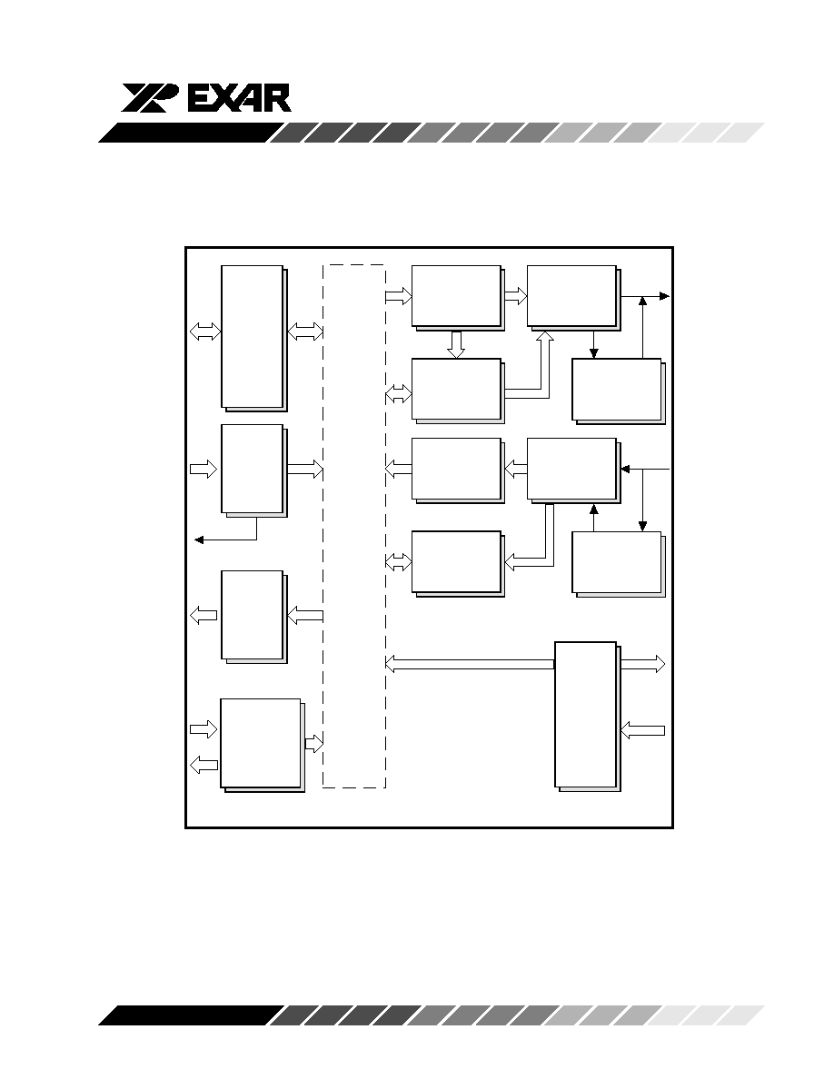
Figure 2. BLOCK DIAGRAM (STANDARD MODE)
XR16C850
4
Rev. 1.20
D0-D7
-IOR
-IOW
A0-A9
-AEN
S1, S2,S3
IRQA
IRQB
IRQC
D
ata
b
u
s
&
C
o
n
trol L
o
g
i
c
R
e
giste
r
Sel
e
c
t
Lo
gic
In
te
rru
p
t
C
o
n
trol
Lo
gic
De
c
o
d
e
Lo
gic
-LPT1
-LPT2
-DTR,-RTS
-CTS
-RI
-CD
-DSR
TX
RX
Modem
Control
Logic
Transmit
FIFO
Registers
Flow
Control
Logic
Transmit
Shift
Register
Receive
FIFO
Registers
Flow
Control
Logic
Receive
Shift
Register
In
te
r C
o
n
n
e
c
t
B
u
s
Lin
e
s
&
C
o
n
trol si
g
n
a
l
s
Clock
&
Baud Rate
Generator
XT
AL
1
XT
AL
2
Ir
Encoder
Ir
Decoder
SEL
GND
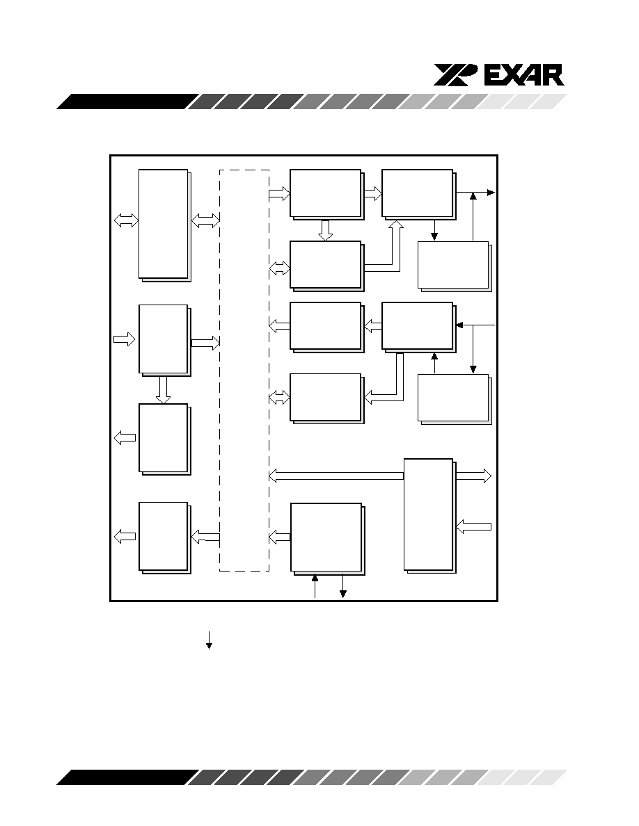
Figure 3. BLOCK DIAGRAM (PC MODE)

XR16C850
5
Rev. 1.20
A0
28
31
28
31
I
Address-0 Select Bit - Internal registers address
selection in PC and STD modes.
A1
27
30
27
30
I
Address-1 Select Bit Internal registers address
selection in PC and STD modes
A2
26
29
26
29
I
Address-2 Select Bit Internal registers address
selection in PC and STD modes
A3 / IOR
22
25
20
22
I
Address-3 Select Bit or Input/Output Read (dual
function) - When the PC mode is selected, this pin
is used as 4th address line to decode the COM1-4
and LPT ports. During STD mode operation this pin
is used as Read strobe. Its function is the same as
-IOR (see -IOR), except it is active high. Either an
active -IOR or IOR is required to transfer data from
850 to CPU during a read operation. Connect this
pin to GND when ≠IOR is used.
A4
-
12
6
6
I
Address-4 Select Bit (internal pull-up) - When the
PC mode is selected, this pin is used as 5th address
line to decode the COM1-4 and LPT ports. This pin
has no function in the STD mode.
A5 / CS0
12
14
9
9
I
Address-5 Select Bit or Chip Select-0 (dual function)
- When the PC mode is selected, this pin is used as
6th address line to decode the COM1-4 and LPT
ports. During STD mode a logical 1 on this pin
provides the chip select 0 function. Connect this pin
to VCC when CS1 or ≠CS2 is used.
A6 / CS1
13
15
10
10
I
Address-6 Select Bit or Chip Select-1 (dual function)
- When the PC mode is selected, this pin is used as
7th address line to decode the COM1-4 and LPT
ports. During STD mode a logical 1 on this pin
provides the chip select 1 function. Connect this pin
to VCC when CS0 or ≠CS2 is used.
A7 / -CS2
14
16
11
7
I
Address-7 Select Bit or Chip Select -2 (dual func-
tion) - When the PC mode is selected, this pin is
used as 8th address line to decode the COM1-4 and
LPT ports. During STD mode a logical 1 on this pin
provides the chip select 2 function. Connect this pin
Symbol
Pin
Signal
Pin Description
40
44
48
52
type
SYMBOL DESCRIPTION

XR16C850
6
Rev. 1.20
to GND when CS0 or CS1 is used.
A8 / IOW
19
21
17
18
I
Address-8 Select Bit or Input/Output Write (dual
function) - When the PC mode is selected, this pin
is used as 9th address line to decode the COM1-4
and LPT ports. During STD mode, a logic 1 transition
creates a write strobe. Its function is the same as -
IOW (see -IOW), but it acts as an active high input
signal. Either -IOW or IOW is required to transfer
data from the CPU to 850 during a write operation.
Connect this pin to GND when ≠IOW is used.
A9
-
1
37
40
I
Address-9 Select Bit (internal pull-up) - When the
PC mode is selected, this pin is used as 10th
address line to decode the COM1-4 and LPT ports.
This pin has no function in the STD mode.
-AEN / -AS
25
28
24
26
I
Address Enable or Address Strobe (dual function) -
. During PC mode operation, valid COM1-4 ports are
decoded when -AEN transitions to a logic 0. During
the STD mode a logic 0 transition on -AS latches the
state of the chip selects and the register select bits,
A0-A2. This input is used when address and chip
selects are not stable for the duration of a read or
write operation, i.e., a microprocessor that needs to
demultiplex the address and data bits. If not re-
quired, the -AS input can be permanently tied to
GND (it is edge triggered).
-BAUDOUT
(See LPT-1)
D0-D7
1-8
2-9
43-47
47-51
2-4
2-4
I/O
Data Bus (Bi-directional) - These pins are the eight
bit, three state data bus for transferring information
to or from the controlling CPU. D0 is the least
significant bit and the first data bit in a transmit or
receive serial data stream.
D10, D11,
-
-
48,1
52,1
D12
22
24
O
High order data bus. When 16 bit data bus (BUS8/
16 = logic zero) is selected, received data errors
(parity, framing, break) can be read along with its
data byte on these pins. D10 is parity error bit, D11
Symbol
Pin
Signal
Pin Description
40
44
48
52
type
SYMBOL DESCRIPTION

XR16C850
7
Rev. 1.20
is framing error bit and D12 is the break bit.
BUS8/16
-
-
25
28
I
8 or 16 Bit Bus select (internal pull-up). For normal
8 bit data bus operation this pin should be connected
to VCC. Connect this pin to GND for 16 bit data bus
operation where RX data errors (parity, framing and
break) are presented on the data bus as D10, D11
and D12 along with the data byte.
CLK8/16
-
-
-
27
I
Transmit / Receive data sampling clock rate (inter-
nal pull-up). For normal operation this pin should be
connected to VCC for 16X sampling clock (stan-
dard). Connect to GND for 8X sampling to double the
data rates.
DRQ
-
-
-
32
O
Receive DMA Request. A Receive ready request is
generated by bringing a RxDRQ line to a high level.
DRQ line is held high until the corresponding DMA
acknowledge (-DACK) line goes low.
-DACK
-
-
-
46
I
DMA Acknowledge Bit (internal pull-up). DMA cycle
will start processing when CPU/Host sets this input
to low. Connect this pin to VCC when not used.
-DDIS
(See LPT-2)
GND
20
22
18
19
Pwr
Signal and Power Ground.
INT
(See IRQA)
-IOR
21
24
19
21
I
Input/Output Read (active low strobe). A logic 0 on
this pin transfers the contents of the 850 data bus to
the CPU. Connect this pin to VCC when IOR is used.
-IOW
18
20
16
17
I
Input/Output Write (active low strobe) - A logic 0 on
this pin transfers the contents of the CPU data bus
to the addressed internal register. Connect this pin
to VCC when IOW is used.
IRQA / INT
30
33
30
33
O
Interrupt Request "A" or Interrupt (three state, open
source, active high) - During PC mode of operation,
this pin functions as IRQA. IRQA is enabled when
Symbol
Pin
Signal
Pin Description
40
44
48
52
type
SYMBOL DESCRIPTION

XR16C850
8
Rev. 1.20
MCR bit-3 is set to a logic 1, interrupts are enabled
in the interrupt enable register (IER), and when an
interrupt condition exists. Interrupt conditions in-
clude: receiver errors, available receiver buffer data,
transmit buffer empty, or when a modem status flag
is detected. During STD mode operation the three
state mode is disabled and this pin functions as INT
(Interrupt Request).
IRQB/-RXRDY
29
32
29
32
O
Interrupt Request "B" or Receive Ready (three state,
dual function) -. During PC mode operation, a logic
1 indicates an interrupt IRQB (see further descrip-
tion under the IRQA). During the STD mode a logic
0 indicates receive data ready status, i.e. the RHR
is full or the FIFO has one or more RX characters
available for unloading. This pin goes to a logic 0
when the FIFO/RHR is full or when there are more
characters available in either the FIFO or RHR.
IRQC/-TXRDY
24
27
23
25
O
Interrupt Request "C" or Transmit Ready (three
state, dual function) - During PC mode operation, a
logic 1 on this pin indicates an interrupt IRQC (see
further description under the IRQA). During the STD
mode buffer ready status is indicated by a logic 0,
i.e., at least one location is empty and available in
the FIFO or THR. This pin goes to a logic 1 when
there are no more empty locations in the FIFO or
THR.
-LPT-1 /
-BAUDOUT
15
17
12
12
O
Baud Rate Generator Output or Line Printer Port-1
Decode Logic Output. (dual function, active low) -
When the PC mode is selected, the baud rate
generator clock output is internally connected to the
RCLK input. This pin then functions as the LPT-1
printer port decode logic output, see table 2. During
STD mode operation, this pin provides the 16X clock
of the selected data rate from the baud rate genera-
tor. The RCLK pin must be connected externally to
-BAUDOUT when the receiver is operating at the
same data rate.
-LPT2/-DDIS
23
26
22
24
O
Drive Disable or Line Printer Port-2 Decode Logic
Output (dual function, active low) - When the PC
Symbol
Pin
Signal
Pin Description
40
44
48
52
type
SYMBOL DESCRIPTION

XR16C850
9
Rev. 1.20
Symbol
Pin
Signal
Pin Description
40
44
48
52
type
SYMBOL DESCRIPTION
mode is selected, this pin functions as the LPT-2
printer port decode logic output, see table 2. During
the STD mode this pin goes to a logic 0 when the
external CPU is reading data from the 850. This
signal can be used to disable external transceivers
or other logic functions. Also, this pin may be D12
signal when BUS16 is selected in 48 and 52 pin
packages.
-OP1/RS485
34
38
34
37
O
Output-1(User Defined) or RS-485 direction control
signal. General purpose output during normal opera-
tion - See bit-2 of modem control register (MCR bit-
2). RS-485 direction control can be selected when
FCTR Bit-3 is set to "1". During data transmit cycle,
-OP1/RS485 pin is low.
-OP2
(See S3)
RCLK
(See S2)
RESET
35
39
35
38
I
Reset. (active high) - A logic 1 on this pin will reset
the internal registers and all the outputs. During
reset, the UART transmitter output and the receiver
input are disabled, the data bus is still controlled by
CS0, CS1, -CS2 and -IOR. (See XR16C850 External
Reset Conditions for initialization details.)
-RXRDY
(See IRQB)
S1
-
23
21
23
I
Port Select-1 (internal pull-up) - When PC mode is
selected, S1 is used in conjunction with S2, S3 and
A3-A9 to select one of the PC COM port addresses
(see Table 2 Internal Address Decode Function)
This pin has no function in the STD mode.
S2 / RCLK
9
10
5
5
I
Port Select-2 or Receive Clock Input (dual function
input with internal pull-up) - When PC mode is
selected, the RCLK input is connected internally to
-BAUDOUT and S2 is used in conjunction with S1,
S3 and A3-A9 to select one of the PC COM port
addresses. During STD mode operation, this pin is
used as external 16X clock input to the receiver
section, normally it's connected to -BAUDOUT.

XR16C850
10
Rev. 1.20
Symbol
Pin
Signal
Pin Description
40
44
48
52
type
SYMBOL DESCRIPTION
S3 / -OP2
31
35
31
34
I/O
Select-3 or User Defined Output-2 (dual function
with internal pull-up) - When PC mode is selected,
S3 is used in conjunction with S1, S2 and A3-A9 to
select one of the PC COM port addresses. In the
STD mode this pin provides the user a general
purpose output. See bit-3 modem control register
(MCR bit-3).
SEL
-
34
36
39
I
Select Mode (internal pull-up) - The PC mode is
selected by a logic 0 (GND) on this pin and STD
mode is selected when this pin is a logic 1 (left open
or tied to VCC). This pin is not available on the 40 pin
PDIP packages which operate in the STD mode
only.
TC
-
-
-
13
I
Terminal Count Bit (internal pull-up). A high pulse
indicates terminal count for any DMA channel is
reached. Connect this pin to GND when not used.
-TXRDY
(See IRQC)
VCC
40
44
42
45
Pwr
Power Supply Input.
XTAL1
16
18
14
15
I
Crystal or External Clock Input - Functions as a
crystal input or as an external clock input. A crystal
can be connected between this pin and XTAL2 to
form an internal oscillator circuit. An external 1 M
resistor is required between the XTAL1 and XTAL2
pins (see figure 9). Alternatively, an external clock
can be connected to this pin to provide custom data
rates (Programming Baud Rate Generator section).
XTAL2
17
19
15
16
O
Output of the Crystal Oscillator or Buffered Clock -
(See also XTAL1). Crystal oscillator output or buff-
ered clock output.
-CD
38
42
40
43
I
Carrier Detect (active low) - A logic 0 on this pin
indicates that a carrier has been detected by the
modem.
-CTS
36
40
38
41
I
Clear to Send (active low) - A logic 0 on the -CTS pin
indicates the modem or data set is ready to accept
transmit data from the 850. Status can be tested by

XR16C850
11
Rev. 1.20
Symbol
Pin
Signal
Pin Description
40
44
48
52
type
SYMBOL DESCRIPTION
reading MSR bit-4. This pin only affects the transmit
and receive operations when Auto CTS function is
enabled via the Enhanced Feature Register (EFR)
bit-7, for hardware flow control operation.
-DSR
37
41
39
42
I
Data Set Ready (active low) - A logic 0 on this pin
indicates the modem or data set is powered-on and
is ready for data exchange with the UART. This pin
has no effect on the UART's transmit or receive
operation.
-DTR
33
37
33
36
O
Data Terminal Ready (active low) - A logic 0 on this
pin indicates that the 850 is powered-on and ready.
This pin can be controlled via the modem control
register. Writing a logic 1 to MCR bit-0 will set the -
DTR output to logic 0, enabling the modem. This pin
will be a logic 1 after writing a logic 0 to MCR bit-0,
or after a reset. This pin has no effect on the UART's
transmit or receive operation.
-RI
39
43
41
44
I
Ring Indicator (active low) - A logic 0 on this pin
indicates the modem has received a ringing signal
from the telephone line. A logic 1 transition on this
input pin will generate an interrupt.
-RTS
32
36
32
35
O
Request to Send (active low) - A logic 0 on the -RTS
pin indicates the transmitter has data ready and
waiting to send. Writing a logic 1 in the modem
control register (MCR bit-1) will set this pin to a logic
0 indicating data is available. After a reset this pin
will be set to a logic 1. This pin only affects the
transmit and receive operations when Auto RTS
function is enabled via the Enhanced Feature Reg-
ister (EFR) bit-6, for hardware flow control operation.
RX / IRRX
10
11
7
7
I
Receive Data - This pin provides the serial receive
data input to the 850. Two user selectable interface
options are available. The first option supports the
standard serial interface. The second option pro-
vides an Infrared decoder interface, see figures 2 and
3. When using the standard modem interface, the
RX input must be a logic 1 during idle (no data

XR16C850
12
Rev. 1.20
or "mark" condition). The inactive state (no data) for
the Infrared decoder interface is a logic 0. MCR bit-
6 selects the standard modem or infrared interface.
During the local loopback mode, the RX pin is
disconnected and TX data is internally connected to
the RX input, see figure 12.
TX / IRTX
11
13
8
8
O
Transmit Data - This pin provides the serial transmit
data from the 850. Two user selectable interface
options are available. The first user option supports
a standard modem interface. The second option
provides an Infrared encoder interface, see figures 2
and 3. When using the standard serial interface, the
TX signal will be a logic 1 during reset, idle (no data),
or when the transmitter is disabled. The inactive
state (no data) for the Infrared encoder interface is a
logic 0. MCR bit-6 selects the standard serial or
infrared interface. During the local loopback mode,
the TX pin is disconnected and TX data is internally
connected to the RX input, see figure 12.
CLKSEL
-
-
13
14
I
Clock Select Bit (internal pull-up). - The 1X or 4X pre-
scaleable clock is selected by this pin. The 1X clock
is selected when CLKSEL is a logic 1 (connected to
VCC) or the 4X is selected when CLKSEL is a logic
0 (connected to GND). MCR bit-7 can override the
state of this pin following reset or initialization (see
MCR bit-7). This pin is not available on 40 and 44 pin
packages which provide MCR bit-7 selection only.
-DMA
-
-
-
20
I
DMA mode enable (internal pull-up). DMA mode is
enabled when this pin is connected to GND. TC, -
DACK, DRQ functions are activated when DMA
mode is selected. TX and RX DMA mode can then
be selected by register EMSR bit 2. Connect this
pin to VCC when DMA mode is not used.
Symbol
Pin
Signal
Pin Description
40
44
48
52
type
SYMBOL DESCRIPTION

XR16C850
13
Rev. 1.20
GENERAL DESCRIPTION
The XR16C850 provides serial asynchronous receive
data synchronization, parallel-to-serial and serial-to-
parallel data conversions for both the transmitter and
receiver sections. These functions are necessary for
converting the serial data stream into parallel data that
is required with digital data systems. Synchronization
for the serial data stream is accomplished by adding
start and stops bits to the transmit data to form a data
character (character orientated protocol). Data integ-
rity is insured by attaching a parity bit to the data
character. The parity bit is checked by the receiver for
any transmission bit errors. The electronic circuitry to
provide all these functions is fairly complex especially
when manufactured on a single integrated silicon chip.
The XR16C850 represents such an integration with
greatly enhanced features. The 850 is fabricated with
an advanced CMOS process.
The 850 is an upward solution that provides 128 bytes
of transmit and receive FIFO memory, instead of 32
bytes provided in the 16C650A, 16 bytes in the 16C550,
or none in the 16C450. The 850 is designed to work with
high speed modems and shared network environ-
ments, that require fast data processing time. In-
creased performance is realized in the 850 by the larger
transmit and receive FIFOs. This allows the external
processor to handle more networking tasks within a
given time. For example, the ST16C550 with a 16 byte
FIFO, unloads 16 bytes of receive data in 1.53 ms (This
example uses a character length of 11 bits, including
start/stop bits at 115.2Kbps). This means the external
CPU will have to service the receive FIFO at 1.53 ms
intervals. However with the 128 byte FIFO in the 850,
the data buffer will not require unloading/loading for 12.2
ms. This increases the service interval giving the
external CPU additional time for other applications and
reducing the overall UART interrupt servicing time. In
addition, the 4 selectable levels of FIFO trigger interrupt
and automatic hardware/software flow control is
uniquely provided for maximum data throughput perfor-
mance especially when operating in a multi-channel
environment. The combination of the above greatly
reduces the bandwidth requirement of the external
controlling CPU, increases performance, and reduces
power consumption.
The 850 provides a RS-485 half-duplex direction control
signal, pin ≠OP1/RS485, to select the external trans-
ceiver direction. It automatically changes the state of
the output pin after the last stop-bit of the last character
has been shifted out for receive state. Afterward, upon
loading a TX data byte it changes state of the output pin
back for transmit state. The RS-485 direction control
pin is not activated after reset. To activate the direction
control function, user has to set EFR Bit-4, and FCTR
Bit-3 to "1". This pin is normally high for receive state,
low for transmit state.
Two data bus interfaces are available to the user. The
PC mode allows direct interconnect to the PC ISA bus
while the STD Mode operates similar to the standard
CPU interface available on the 16C450/550/650A.
When the PC mode is selected, the external logic
circuitry required for PC COM port address decode and
chip select is eliminated. These functions are provided
internally in the 850.
The 850 is capable of operation to 1.5Mbps with a 24
MHz crystal or external clock input. With a crystal of
14.7464 MHz and through a software option, the user
can select data rates up to 460.8Kbps or 921.6Kbps.
The rich feature set of the 850 is available through
internal registers. Automatic hardware/software flow
control, selectable transmit and receive FIFO trigger
levels, selectable TX and RX baud rates, infrared en-
coder/decoder interface, modem interface controls,
and a sleep mode are all standard features. In addition
the 44/48/52 pin packages offer the PC Mode, two
additional three state interrupt lines and one selectable
open source interrupt output. The open source interrupt
scheme allows multiple interrupts to be combined in a
"WIRE-OR" operation, thus reducing the number of
interrupt lines in larger systems. Following a power on
reset or an external reset, the 850 is software compat-
ible with previous generation of UARTs, 16C450,
16C550 and 16C650A.
XR16C850
14
Rev. 1.20
D0
D1
D2
D3
D4
D5
D6
D7
A0
A1
A2
A3
A4
A5
A6
A7
A8
A9
AEN*
IOR*
IOW*
RESET
AD
DR
E
S
S
D
E
C
O
D
E
LO
G
I
C
1
3
5
7
2
4
6
8
J1
HDR2X4
3F8
2F8
3E8
2E8
D0
D1
D2
D3
D4
D5
D6
D7
-IOR
-IOW
A0
A1
A2
-CS2
RESET
VCC
CS0
CS1
-AS
IOR
IOW
IRQ3
INT
1
2
3
U2A
74LS125A
-OP2
RCLK
-BAUDOUT
1
3
2
4
J2
HDR2X2
IRQ4
SEL
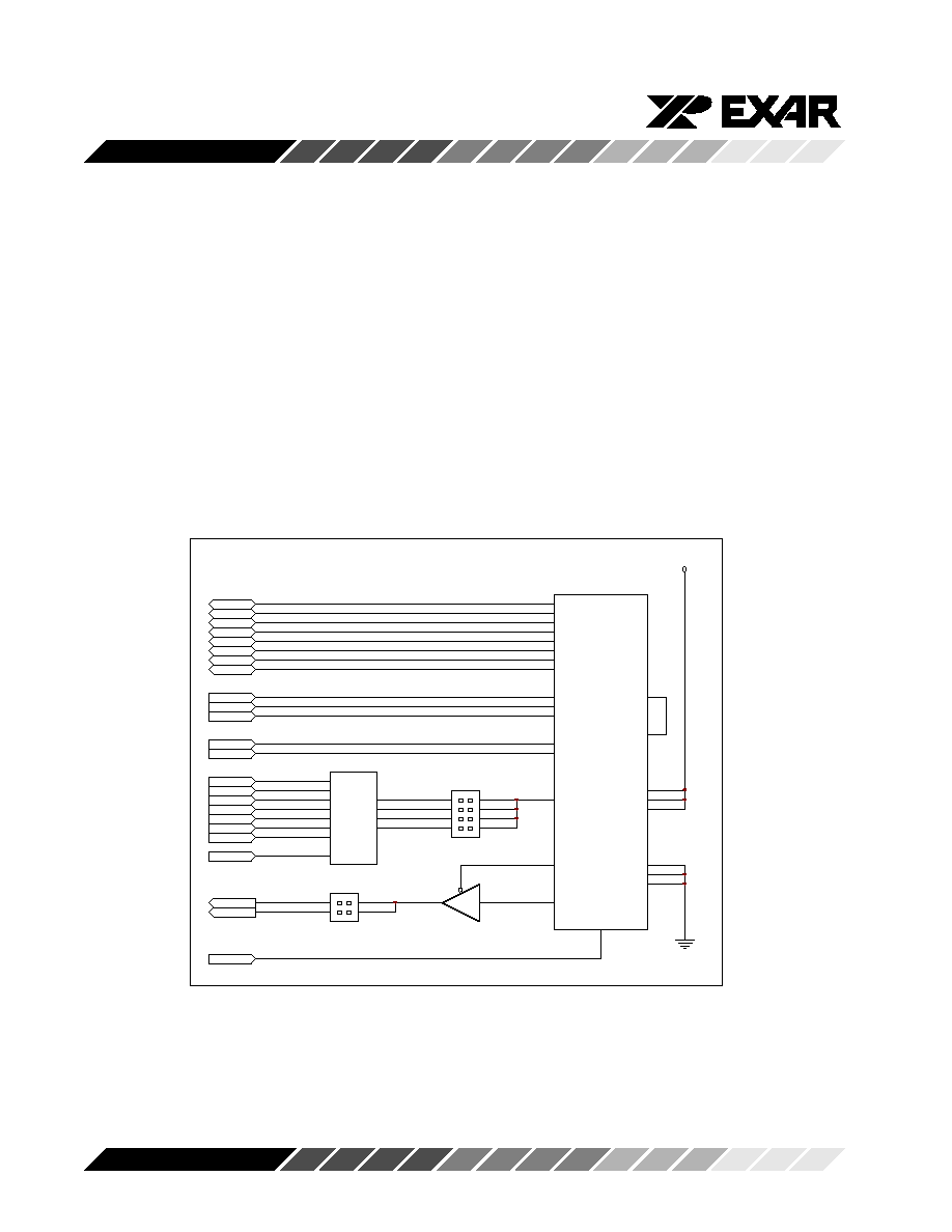
FUNCTIONAL DESCRIPTIONS
Interface Options
Standard 16550 Mode Interface
The 850 provides a pin compatible interface for emula-
tion of the 16C550 when in the STD mode. The STD
mode is selected by making the SEL pin a logic 1
(VCC). When the SEL pin is set to a logic 1, the 850
interface is the same as Industry Standard 16C550.
Figure 4 shows a typical connection to the PC ISA bus.
Figure 4, STANDARD MODE INTERFACE
XR16C850
15
Rev. 1.20
D0
D1
D2
D3
D4
D5
D6
D7
A0
A1
A2
A3
A4
A5
A6
A7
A8
A9
AEN*
IOR*
IOW*
RESET
D0
D1
D2
D3
D4
D5
D6
D7
-IOR
-IOW
A0
A1
A2
RESET
A3
A4
A5
A6
A7
A8
A9
-AEN
1
3
5
2
4
6
J1
HDR2X3
S1
S2
S3
IRQ4
IRQ3
IRQn
INTA
INTB
INTC
SEL
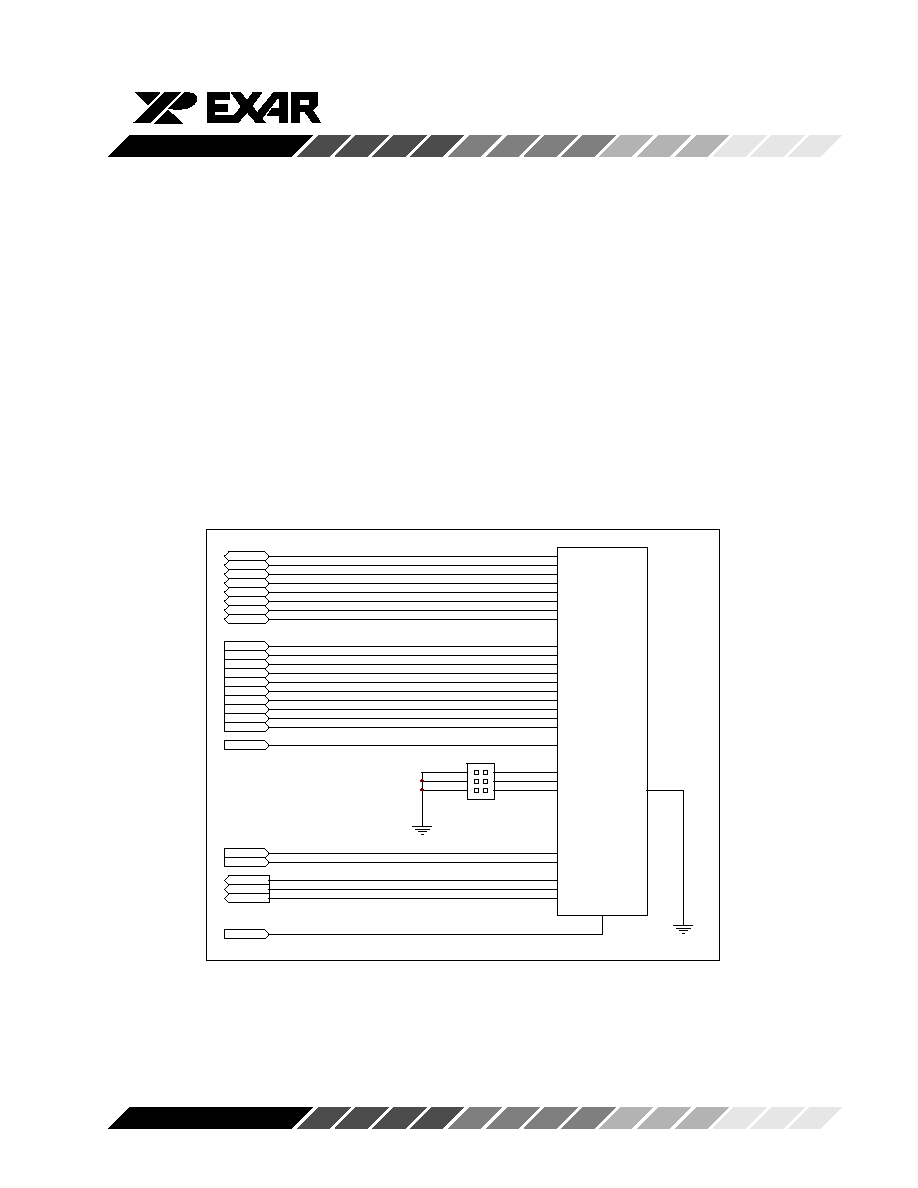
PC Mode Interface (available on 44/48/52 pin ver-
sions only)
The PC mode is selected by making the SEL pin a logic
0 (GND). When the PC mode is selected, the 850
eliminates the external address decode logic circuitry
that is required. The PC mode is accomplished by
decoding the PC ISA bus address bits, A3 through A9
inside the 850. These addresses select the standard
PC COM ports: COM-1 (3F8-3FF Hex), COM-2 (2F8-
2FF Hex), COM-3 (3E8-3EF Hex), and COM-4 (2E8-
2EF Hex). Three inputs (S1-S3) are generally exter-
nally jumpered (logic 1 or logic 0) for selecting the oper
ating port. The selection bits are also associated with
a given PC interrupt. Interrupts IRQA, IRQB, and IRQC
function as three state outputs. MCR bit-3 must be set
to a logic 1 to activate these interrupts. The mapping for
the COM port 1-4 and their associated interrupt selec-
tions, IRQx are listed in Table 2, below. Figure 5 shows
a typical connection to the PC ISA bus.
In addition to the COM port addresses, the 850 de-
codes two additional printer addresses. These address
decodes select LPT-1 (printer port-1, 378-37F Hex), or
LPT-2 (printer port-2, 278-27F Hex). These ports are
intended to be compatible with PC or PC compatible
computer printer ports.
Figure 5. PC MODE INTERFACE

XR16C850
16
Rev. 1.20
SEL S3 S2 S1
A3-A9
COM Port
Selected IRQ *2
0
0
0
0
3F8-3FF
COM-1
IRQB (IRQ4)
0
0
0
1
2F8-2FF
COM-2
IRQC (IRQ3)
0
0
1
0
3E8-3EF
COM-3
IRQB (IRQ4)
0
0
1
1
2E8-2EF
COM-4
IRQC (IRQ3)
0
1
0
0
3F8-3FF
COM-1
IRQA (IRQn)
0
1
0
1
2F8-2FF
COM-2
IRQA (IRQn)
0
1
1
0
3E8-3EF
COM-3
IRQA (IRQn)
0
1
1
1
2E8-2EF
COM-4
IRQA (IRQn)
0
-
-
-
278-27F
LPT-2
N/A
0
-
-
-
378-37F
LPT-1
N/A
Table 2. PC MODE INTERNAL ADDRESS DECODE FUNCTIONS
Note *2: All interrupt outputs are inactive (three state mode) except when the selected address range is valid.
XR16C850
17
Rev. 1.20
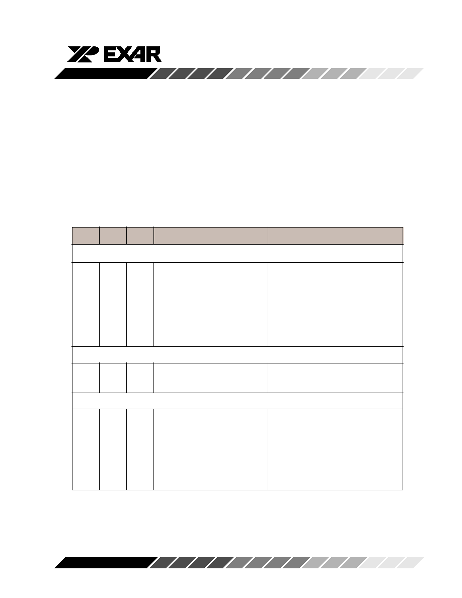
Internal Registers
The 850 provides 15 internal registers for monitoring and
control. These registers are shown in Table 3 below.
Twelve registers are similar to those already available in
the standard 16C550. These registers function as data
holding registers (THR/RHR), interrupt status and con-
trol registers (IER/ISR), a FIFO control register (FCR),
line status and control registers, (LCR/LSR), modem
status and control registers (MCR/MSR), program-
mable data rate (clock) control registers (DLL/DLM),
and a user assessable scratchpad register (SPR).
Beyond the general 16C550 features and capabilities,
the 850 offers an enhanced feature register set called
EFR, Xon/Xoff 1-2, TRG, FCTR, and EMSR. Register
functions are more fully described in the following
paragraphs.
A2
A1
A0
READ MODE
WRITE MODE
General Register Set (THR/RHR, IER/ISR, MCR/MSR, LCR/LSR, SPR):
0
0
0
Receive Holding Register
Transmit Holding Register
0
0
1
Interrupt Enable Register
0
1
0
Interrupt Status Register
FIFO Control Register
0
1
1
Line Control Register
1
0
0
Modem Control Register
1
0
1
Line Status Register
1
1
0
Modem Status Register
1
1
1
Scratchpad Register
Scratchpad Register
Baud Rate Register Set (DLL/DLM): Note *3
0
0
0
LSB of Divisor Latch
LSB of Divisor Latch
0
0
1
MSB of Divisor Latch
MSB of Divisor Latch
Enhanced Register Set (Xon/off 1-2, TRG, FCTR, EFR, EMSR): Note *4
0
0
0
FIFO Trigger Register
FIFO trigger counter
0
0
1
Feature Control Register
0
1
0
Enhanced Feature Register
Enhanced Feature Register
1
0
0
Xon-1 Word
Xon-1 Word
1
0
1
Xon-2 Word
Xon-2 Word
1
1
0
Xoff-1 Word
Xoff-1 Word
1
1
1
Xoff-2 Word
Xoff-2 Word
1
1
1
Enhanced Mode Select Register
Table 3. INTERNAL REGISTERS
Note *3: These registers are accessible only when LCR bit-7 is set to a logic 1.
Note *4: Enhanced Feature Registers are accessible only when the LCR is set to "BF" hex.

XR16C850
18
Rev. 1.20
FIFO Operation
The 128 byte transmit and receive data FIFO's are
enabled by the FIFO Control Register (FCR) bit-0. With
16C550 devices, the user can only set the receive
trigger level but not the transmit trigger level. The 850
provides independent trigger levels for both receiver and
transmitter. To remain compatible with 16C550, the
transmit interrupt trigger level is set to 16 following a
reset. It should be noted that the user can set the
transmit trigger levels by writing to the FCR register, but
activation will not take place until EFR bit-4 is set to a
logic 1. The receiver FIFO section includes a time-out
function to ensure data is delivered to the CPU. An
interrupt is generated whenever the Receive Holding
Register (RHR) has not been read following the loading
of a character or the receive trigger level has not been
reached. (see hardware flow control for a description of
this timing).
Hardware Flow Control
When automatic hardware flow control is enabled, the
850 monitors the -CTS pin for a remote buffer overflow
indication and controls the -RTS pin for local buffer
overflows. Automatic hardware flow control is selected
by setting bits 6 (RTS) and 7 (CTS) of the EFR register
to a logic 1. If -CTS transitions from a logic 0 to a logic
1 indicating a flow control request, ISR bit-5 will be set
to a logic 1 (if enabled via IER bit 6-7), and the 850 will
suspend TX transmissions as soon as the stop bit of the
character in process is shifted out. Transmission is
resumed after the -CTS input returns to a logic 0,
indicating more data may be sent.
The 850 has a new feature that provides flow control
trigger hysteresis while maintains compatibility to
16C650A and 16C550. With the Auto RTS function
enabled, an interrupt is generated when the receive
FIFO reaches the programmed RX trigger level. The -
RTS pin will not be forced to a logic 1 (RTS Off), until the
receive FIFO reaches the upper limit of the hysteresis
level. The -RTS pin will return to a logic 0 after the RX
data buffer (FIFO) is unloaded to the lower limit of the
hysteresis level. Under the above described conditions
the 850 will continue to accept data until the receive
FIFO gets full. The Auto RTS function is initiated when
the ≠RTS output pin is asserted to logic 0 (RTS On).
Below shows the 650A and 850 hysteresis level of "N"
with respect to Auto RTS flow control levels.
FCTR
Trigger
RTS
INT
-RTS
-RTS
Bit-1 and 0
Level
Hysteresis
Pin
De-asserted
Asserted
Selection
(characters)
(characters)
Activation at
(characters)
(characters)
00
8
8
16
0
00
16
16
24
8
00
24
24
28
16
00
28
28
28
24
01
N
+/-4
N
N plus 4
N minus 4
10
N
+/-6
N
N plus 6
N minus 6
10
N
+/-6
N
N plus 6
N minus 6

XR16C850
19
Rev. 1.20
Software Flow Control
When software flow control is enabled, the 850 com-
pares one or two sequential receive data characters with
the programmed Xon or Xoff-1,2 character value(s). If
receive character(s) (RX) match the programmed val-
ues, the 850 will halt transmission (TX) as soon as the
current character(s) has completed transmission.
When a match occurs, the receive ready (if enabled via
Xoff IER bit-5) flags will be set and the interrupt output
pin (if receive interrupt is enabled) will be activated.
Following a suspension due to a match of the Xoff
characters values, the 850 will monitor the receive data
stream for a match to the Xon-1,2 character value(s). If
a match is found, the 850 will resume operation and
clear the flags (ISR bit-4).
Reset initially sets the contents of the Xon/Xoff 8-bit flow
control registers to a logic 0. Following reset the user
can write any Xon/Xoff value desired for software flow
control. Different conditions can be set to detect Xon/
Xoff characters and suspend/resume transmissions.
When double 8-bit Xon/Xoff characters are selected, the
850 compares two consecutive receive characters with
two software flow control 8-bit values (Xon1, Xon2, Xoff1,
Xoff2) and controls TX transmissions accordingly. Un-
der the above described flow control mechanisms, flow
control characters are not placed (stacked) in the user
accessible RX data buffer or FIFO.
In the event that the receive buffer is overfilling and flow
control needs to be executed, the 850 automatically
sends an Xoff message (when enabled) via the serial TX
output to the remote modem. The 850 sends the Xoff-1,2
characters as soon as received data passes the pro-
grammed trigger level. To clear this condition, the 850
will transmit the programmed Xon-1,2 characters as
soon as receive data drops below the programmed
trigger level.
Special Feature Software Flow Control
A special feature is provided to detect an 8-bit character
when bit-5 is set in the Enhanced Feature Register
(EFR). When this character is detected, it will be placed
on the user accessible data stack along with normal
incoming RX data. This condition is selected in conjunc-
tion with EFR bits 0-3. Note that software flow control
should be turned off when using this special mode by
setting EFR bit 0-3 to a logic 0.
The 850 compares each incoming receive character
with Xoff-2 data. If a match exists, the received data will
be transferred to FIFO and ISR bit-4 will be set to
indicate detection of special character (see Figure 9).
Although the Internal Register Table shows each X-
Register with eight bits of character information, the
actual number of bits is dependent on the programmed
word length. Line Control Register (LCR) bits 0-1 defines
the number of character bits, i.e., either 5 bits, 6 bits, 7
bits, or 8 bits. The word length selected by LCR bits 0-
1 also determines the number of bits that will be used
for the special character comparison. Bit-0 in the X-
registers corresponds with the LSB bit for the receive
character.
Time-out Interrupts
Three special interrupts have been added to monitor the
hardware and software flow control. The interrupts are
enabled by IER bits 5-7. Care must be taken when
handling these interrupts. Following a reset the trans-
mitter interrupt is enabled, the 850 will issue an interrupt
to indicate that transmit holding register is empty. This
interrupt must be serviced prior to continuing opera-
tions. The LSR register provides the current singular
highest priority interrupt only. It could be noted that CTS
and RTS interrupts have lowest interrupt priority. A
condition can exist where a higher priority interrupt may
mask the lower priority CTS/RTS interrupt(s). Only after
servicing the higher pending interrupt will the lower
priority CTS/ RTS interrupt(s) be reflected in the status
register. Servicing the interrupt without investigating
further interrupt conditions can result in data errors.
When two interrupt conditions have the same priority, it
is important to service these interrupts correctly. Re-
ceive Data Ready and Receive Time Out have the same
interrupt priority (when enabled by IER bit-0). The
receiver issues an interrupt after the number of charac-
ters have reached the programmed trigger level. In this
case the 850 FIFO may hold more characters than the
programmed trigger level. Following the removal of a
data byte, the user should recheck LSR bit-0 for
additional characters. A Receive Time Out will not occur
if the receive FIFO is empty. The time out counter is
reset at the center of each stop bit received or each time
the receive holding register (RHR) is read. The actual
time out value is T (Time out length in bits) = 4 X P
XR16C850
20
Rev. 1.20
C1
22pF
C2
33pF
X1
1.8432 MHz
R1
50-120
R2
1M
XT
A
L
1
XT
A
L
2
(Programmed word length) + 12. To convert the time out
value to a character value, the user has to consider the
complete word length, including data information
length, start bit, parity bit, and the size of stop bit, i.e.,
1X, 1.5X, or 2X bit times.
Example -A: If the user programs a word length of 7, with
no parity and one stop bit, the time out will be:
T = 4 X 7( programmed word length) +12 = 40 bit times.
The character time will be equal to 40 / 9 = 4.4
characters, or as shown in the fully worked out example:
T = [(programmed word length = 7) + (stop bit = 1) +
(start bit = 1) = 9]. 40 (bit times divided by 9) = 4.4
characters.
Example -B: If the user programs the word length = 7,
with parity and one stop bit, the time out will be:
T = 4 X 7(programmed word length) + 12 = 40 bit times.
Character time = 40 / 10 [ (programmed word length =
7) + (parity = 1) + (stop bit = 1) + (start bit = 1) = 4
characters.
Due to limitations involved in servicing a number of
simultaneous interrupts in PCs and multi-channel sys-
tems, the 850 offers shared wire-or interrupts by setting
MCR bit-5 to a logic 1. When using this mode, the
connection of a 200-500 ohm resistor is required be-
tween the IRQA/INT pin and signal ground to provide an
acceptable logic 0 level. The other interrupts (IRQB,
IRQC) are inactive when using this mode.
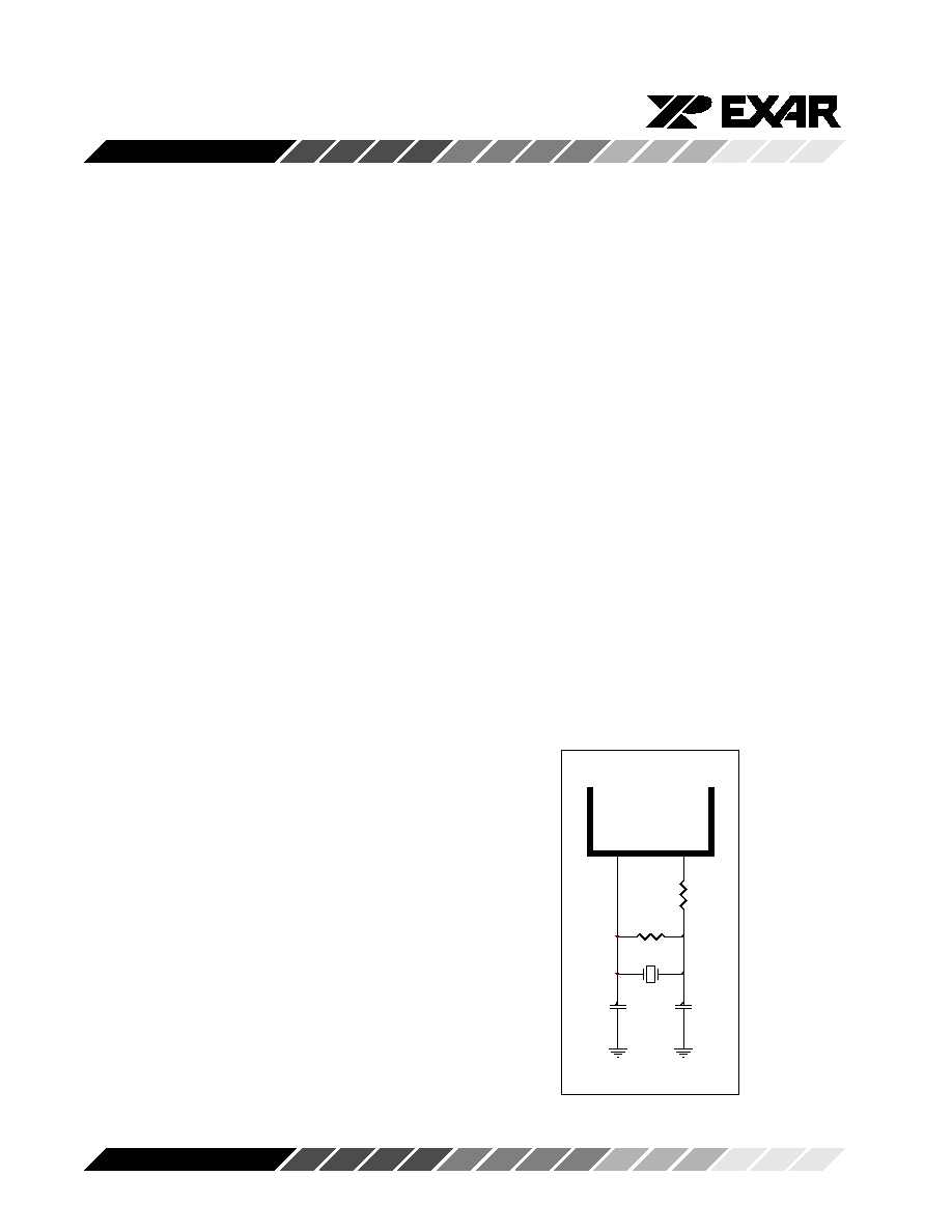
Programmable Baud Rate Generator
The 850 supports high speed modem technologies that
have increased input data rates by employing data
compression schemes. For example a 33.6Kbps mo-
dem that employs data compression may require a
115.2Kbps input data rate. A 128.0Kbps ISDN modem
that supports data compression may need an input data
rate of 460.8Kbps. The 850 can support a standard data
rate of 921.6Kbps with a crystal of 14.7456MHz.
A single baud rate generator is provided for the transmit-
ter and receiver, allowing independent TX/RX channel
control. The programmable Baud Rate Generator is
capable of accepting an input clock up to 24 MHz, as
required for supporting a 1.5Mbps data rate. The 850
can be configured for internal or external clock opera-
tion. For internal clock oscillator operation, an industry
standard microprocessor crystal (parallel resonant/ 22-
33 pF load) is connected externally between the XTAL1
and XTAL2 pins, with an external 500K to 1 M
resistor
across it. The serial 50-120
resistor on pin XTAL2 may
be deleted for high frequency crystal operation
.
Alterna-
tively, an external clock can be connected to the XTAL1
pin to clock the internal baud rate generator for standard
or custom rates.
The generator divides the input 16X clock by any divisor
from 1 to 2
16
-1. The 850 divides the basic crystal or
external clock by 16. Further division of this 16X clock
provides two table rates to support low and high data
rate applications using the same system design. The
two rate tables are selectable through the internal
register, MCR bit-7. Setting MCR bit-7 to a logic 1
provides an additional divide by 4 whereas, setting MCR
bit-7 to a logic 0 only divides by 1. (See Table 4 and
Figure 11). The frequency of the -BAUDOUT output pin
is exactly 16X (16 times) of the selected baud rate (-
BAUDOUT =16 x Baud Rate). Customized Baud Rates
can be achieved by selecting the proper divisor values
for the MSB and LSB sections of baud rate generator.
Programming the Baud Rate Generator Registers DLM
(MSB) and DLL (LSB) provides a user capability for
selecting the desired final baud rate. The example in
Table 4 below, shows the two selectable baud rate
tables available when using a 7.3728 MHz crystal.
XR16C850
21
Rev. 1.20
Divide
by
1 logic
XTAL1
XTAL2
Divide
by
4 logic
Clock
Oscillator
Logic
Baudrate
Generator
Logic
-BAUDOUT
MCR
Bit-7=0
MCR
Bit-7=1
Output
Output
User
User
DLM
DLL
Baud Rate
Baud Rate
16 x Clock
16 x Clock
Program
Program
MCR
MCR
Divisor
Divisor
Value
Value
BIT-7=1
Bit-7=0
(Decimal)
(HEX)
(HEX)
(HEX)
50
200
2304
900
09
00
75
300
1536
600
06
00
150
600
768
300
03
00
300
1200
384
180
01
80
600
2400
192
C0
00
C0
1200
4800
96
60
00
60
2400
9600
48
30
00
30
4800
19.2K
24
18
00
18
7200
28.8K
16
10
00
10
9600
38.4k
12
0C
00
0C
19.2k
76.8k
6
06
00
06
38.4k
153.6k
3
03
00
03
57.6k
230.4k
2
02
00
02
115.2k
460.8k
1
01
00
01
Figure 11. Baud Rate Generator Circuitry
Table 4. BAUD RATE GENERATOR PROGRAMMING TABLE (7.3728 MHz CLOCK)

XR16C850
22
Rev. 1.20
DMA Operation
The 850 FIFO trigger level provides additional flexibility
to the user for block transfer operation. LSR bits 5-6
provide an indication when the transmitter is empty or
has an empty location(s). The user can optionally
operate the transmit and receive FIFOs in the DMA
mode (FCR bit-3). When the transmit and receive FIFOs
are enabled and the DMA mode is deactivated (DMA
Mode "0"), the 850 activates the interrupt output pin for
each data transmit or receive operation. When DMA
mode is activated (DMA Mode "1"), the user takes the
advantage of block mode operation by loading or unload-
ing the FIFO in a block sequence determined by the
preset trigger level. In this mode, the 850 sets the
interrupt output pin when characters in the transmit
FIFOs are below the transmit trigger level, or the
characters in the receive FIFOs are above the receive
trigger level. Transmit or receive DMA operation is
selected by EMSR register bit 2.
Sleep Mode
The 850 is designed to operate with low power con-
sumption. A sleep mode is included to further reduce
power consumption when the chip is not being used.
The operating parameters are maintained while in sleep
mode. With EFR bit-4 and IER bit-4 enabled (set to a
logic 1), the 850 enters the sleep mode when no
interrupt is pending and no activities on the modem port.
If an external clock is supplied to the 850, you may want
to stop it. The 850 resumes normal operation when a RX
character's start bit is detected, a change of state on
any of the modem input pins RX, -RI, -CTS, -DSR, -CD,
or transmit data is loaded into the FIFO by the user. It
typically takes 30us for the crystal oscillator to restart
from sleep mode depending on the crystal properties.
This delay must be taken into consideration during
design as Rx character(s) may be lost since it depends
on the operating bit rate. If the sleep mode is enabled
and the 850 is awakened by one of the conditions
described above, it will return to the sleep mode auto-
matically after the last character is transmitted or read
by the user and no interrupt is pending. In any case, the
chip will not enter sleep mode while an interrupt(s) is still
pending and the oscillator would still be running. The
850 will stay in the sleep mode of operation until it is
disabled by setting IER bit-4 to a logic 0.
Sleep mode enable during initialization example:
Write LCR with "BF" hex
; access to EFR registers
Set EFR bit-4 to logic 1
; enable enhanced function bits
Write LCR with op. value
; set LCR with op. parameters
Set IER bit-4 to logic 1
; enable sleep mode.
; It goes to sleep when:
; no pending interrupt,
; no modem port activity then enters
; sleep mode by stopping osc.
For lowest sleep current the following pins should be left at logic
1 state: S1, S2, A4, A9, BUS8/16, CLK8/16, CLKSEL, -DMA, -DACK,
SEL, TC and RX.
Loopback Mode
The internal loopback capability allows onboard diag-
nostics. In this mode, the normal modem interface pins
are disconnected and reconfigured for loopback inter-
nally. MSR bits 4-7 are also disconnected. However,
MCR register bits 0-3 can be used for controlling
loopback diagnostic testing. In this mode, OP1 and
OP2 in the MCR register (bits 0-1) control the modem
-RI and -CD inputs respectively. MCR signals -DTR and
-RTS (bits 0-1) are used to control the modem -CTS and
-DSR inputs respectively. The transmitter output (TX)
and the receiver input (RX) are disconnected from their
associated interface pins, and instead are connected
together internally (See Figure 12). The -CTS, -DSR,
-CD, and -RI are disconnected from their normal
modem control inputs pins, and instead are connected
internally to -DTR, -RTS, -OP1 and -OP2. Loopback test
data is entered into the transmit holding register via the
user data bus interface, D0-D7. The transmit UART
serializes the data and passes the serial data to the
receive UART via the internal loopback connection. The
receive UART converts the serial data back into parallel
data that is then made available at the user data
interface, D0-D7. The user optionally compares the
received data to the initial transmitted data for verifying
error free operation of the UART TX/RX circuits. In this
mode, the receiver, transmitter and modem control
interrupts are fully operational. However, the interrupts
can only be read using lower four bits of the Modem
Control Register (MCR bits 0-3) instead of the four
Modem Status Register bits 4-7. The interrupts are still
controlled by the IER.

XR16C850
23
Rev. 1.20
D0-D7
-IOR,IOR
-IOW,IOW
RESET
A0-A2
-AS
CS0,CS1
-CS2
INT
-RXRDY
-TXRDY
TX
RX
Da
ta
bu
s
&
C
o
n
t
r
ol Lo
gi
c
R
e
g
is
te
r
Sel
ect
Lo
gi
c
M
o
de
m
C
o
n
t
r
ol L
ogi
c
In
t
e
rr
u
p
t
C
o
n
tro
l
Lo
gi
c
Transmit
FIFO
Registers
Flow
Control
Logic
Transmit
Shift
Register
Receive
FIFO
Registers
Flow
Control
Logic
Receive
Shift
Register
I
n
t
e
r
Co
n
n
e
c
t
Bu
s
L
i
n
e
s
&
C
o
n
t
ro
l
sig
n
a
l
s
Cl
o
c
k
&
Ba
u
d
Ra
t
e
Ge
n
e
r
a
tor
XTAL1
RCLK
XTAL2
-BAUDOUT
-DDIS
Ir
Encoder
Ir
Decoder
-CTS
-RTS
-DTR
-DSR
-RI
-CD
-OP1
-OP2
MCR
Bi
t
-
4
=
1
Figure 12. INTERNAL LOOPBACK MODE DIAGRAM

XR16C850
24
Rev. 1.20
REGISTER FUNCTIONAL DESCRIPTIONS
The following table delineates the assigned bit functions for the fifteen 850 internal registers. The assigned bit
functions are more fully defined in the following paragraphs.
XR16C850 ACCESSIBLE REGISTERS
A2 A1 A0
Register
BIT-7
BIT-6
BIT-5
BIT-4
BIT-3
BIT-2
BIT-1
BIT-0
[Default]
Note *3
General Registers are accessible when LCR bit-7 is not a Logic 1 or "BF" Hex
0
0
0
RHR [XX]
bit-7
bit-6
bit-5
bit-4
bit-3
bit-2
bit-1
bit-0
0
0
0
THR [XX]
bit-7
bit-6
bit-5
bit-4
bit-3
bit-2
bit-1
bit-0
0
0
1
IER [00]
0/
0/
0/
0/
modem
receive
transmit
receive
-CTS
-RTS
Xoff
Sleep
status
line
holding
holding
interrupt
interrupt
interrupt
mode
interrupt
status
register
register
interrupt
0
1
0
FCR [00]
RCVR
RCVR
0/TX
0/TX
DMA
XMIT
RCVR
FIFO
trigger
trigger
trigger
trigger
mode
FIFO
FIFO
enable
(MSB)
(LSB)
(MSB)
(LSB)
select
reset
reset
0
1
0
ISR [01]
0/
0/
0/
0/
int
int
int
int
FIFO's
FIFO's
-RTS,
Xoff
priority
priority
priority
status
enabled
enabled
-CTS
bit-2
bit-1
bit-0
0
1
1
LCR [00]
divisor
set
set
even
parity
stop
word
word
latch
break
parity
parity
enable
bits
length
length
enable
bit-1
bit-0
1
0
0
MCR [00]
Clock
0/
0/
loop
-OP2
-OP1
-RTS
-DTR
select
IRRT
Xon
back
enable
Any
1
0
1
LSR [60]
0/
trans.
trans.
break
framing
parity
overrun
receive
FIFO
empty
holding
interrupt
error
error
error
data
error
empty
ready
1
1
0
MSR [00]
-CD
-RI
-DSR
-CTS
delta
delta
delta
delta
-CD
-RI
-DSR
-CTS
1
1
1
SCPAD [FF]
bit-7
bit-6
bit-5
bit-4
bit-3
bit-2
bit-1
bit-0
Baud rate generator registers are accessible only when LCR bit-7 is set to Logic 1.
0
0
0
DLL [00]
bit-7
bit-6
bit-5
bit-4
bit-3
bit-2
bit-1
bit-0
0
0
1
DLM [00]
bit-15
bit-14
bit-13
bit-12
bit-11
bit-10
bit-9
bit-8

XR16C850
25
Rev. 1.20
A2 A1 A0
Register
BIT-7
BIT-6
BIT-5
BIT-4
BIT-3
BIT-2
BIT-1
BIT-0
[Default]
Note *3
Enhanced Registers are accessible only when LCR is set to "BF" Hex.
1
0
0
Xon-1[00]
bit-7
bit-6
bit-5
bit-4
bit-3
bit-2
bit-1
bit-0
1
0
1
Xon-2[00]
bit-15
bit-14
bit-13
bit-12
bit-11
bit-10
bit-9
bit-8
1
1
0
Xoff-1[00]
bit-7
bit-6
bit-5
bit-4
bit-3
bit-2
bit-1
bit-0
1
1
1
Xoff-2[00]
bit-15
bit-14
bit-13
bit-12
bit-11
bit-10
bit-9
bit-8
0
0
0
TRG [00]
Trig/
Trig/
Trig/
Trig/
Trig
Trig/
Trig/
Trig/
FC
FC
FC
FC
FC
FC
FC
FC
0
0
1
FCTR [00]
Rx/Tx
SCPAD
Trig
Trig
RS485
IrRx
-RTS
-RTS
M o d e
Swap
Bit-1
Bit-0
Auto
Inv.
Delay
Delay
control
Bit-1
Bit-0
0
1
0
EFR [00]
Auto
Auto
Special
Enable
Cont-3
Cont-2
Cont-1
Cont-0
-CTS
-RTS
Char.
IER
Tx,Rx
Tx,Rx
Tx,Rx
Tx,Rx
select
Bits 4-7,
Control
Control
Control
Control
ISR, FCR
Bits 4-5,
M C R
Bits 5-7
1
1
1
EMSR [00]
Not
Not
Not
Not
Not
Rx/Tx
ALT.
Rx/Tx
Used
Used
Used
Used
Used
D M A
Rx/Tx
FIFO
Select
FIFO
Count
Count
Note *3: The value represents the register's initialized Hex value. An "X" signifies a 4-bit un-initialized nibble.

XR16C850
26
Rev. 1.20
Transmit and Receive Holding Register
The serial transmitter section consists of an 8-bit
Transmit Hold Register (THR) and Transmit Shift Reg-
ister (TSR). The status of the THR is provided in the Line
Status Register (LSR). Writing to the THR transfers the
contents of the data bus (D7-D0) to the THR, providing
that the THR or TSR is empty. The THR empty flag in the
LSR register will be set to a logic 1 when the transmitter
is empty or when data is transferred to the TSR. Note
that a write operation can be performed when the
transmit holding register empty flag is set (logic 0 =
FIFO full, logic 1= at least one FIFO location available).
The serial receive section also contains an 8-bit Receive
Holding Register, RHR. Receive data is removed from
the 850 and receive FIFO by reading the RHR register.
The receive section provides a mechanism to prevent
false starts. On the falling edge of a start or false start
bit, an internal receiver counter starts counting clocks
at 16x clock rate. After 7 1/2 clocks the start bit time
should be shifted to the center of the start bit. At this
time the start bit is sampled and if it is still a logic 0 it
is validated. Evaluating the start bit in this manner
prevents the receiver from assembling a false character.
Receiver status codes will be posted in the LSR.
Device Identification
The XR16C850 provides Device identification and De-
vice Revision code to distinguish the part from others. It
is suggested to read the identification and revision
information from the part only during the power on
initialization routine to avoid disturbing the baud rate
generator.
To read the identification number from the device, it is
required to set the baud rate generator divisor latch to "1"
(LCR bit-7 = logic 1) and set the content of the baud rate
generator DLL and DLM registers to "00" hex. Then read
the content of DLM for "10" hex for XR16C850 and the
content of DLL for the revision of the part.
Interrupt Enable Register (IER)
The Interrupt Enable Register (IER) masks the inter-
rupts from receiver ready, transmitter empty, line status
and modem status registers. These interrupts would
normally be seen on the 850 INT output pin.
IER Vs Receive FIFO Interrupt Mode Operation
When the receive FIFO (FCR BIT-0 = a logic 1) and
receive interrupts (IER BIT-0 = logic 1) are enabled, the
receive interrupts and register status will reflect the
following:
A) The receive data available interrupts are issued to the
external CPU when the FIFO has reached the pro-
grammed trigger level. It will be cleared when the FIFO
drops below the programmed trigger level.
B) FIFO status will also be reflected in the user acces-
sible ISR register when the FIFO trigger level is reached.
Both the ISR register status bit and the interrupt will be
cleared when the FIFO drops below the trigger level.
C) The data ready bit (LSR BIT-0) is set as soon as a
character is transferred from the shift register to the
receive FIFO. It is reset when the FIFO is empty.
IER Vs Receive/Transmit FIFO Polled Mode Opera-
tion
When FCR BIT-0 equals a logic 1; resetting IER bits 0-
3 enables the 850 in the FIFO polled mode of operation.
Since the receiver and transmitter have separate bits in
the LSR either or both can be used in the polled mode
by selecting respective transmit or receive control bit(s).
A) LSR BIT-0 will be a logic 1 as long as there is one byte
in the receive FIFO.
B) LSR BIT 1-4 will indicate if an overrun error occurred
in the receiver.
C) LSR BIT-5 will indicate when the transmit FIFO is
empty.
D) LSR BIT-6 will indicate when both the transmit FIFO
and transmit shift register are empty.
E) LSR BIT-7 will indicate any data errors within the
receive FIFO. This bit will clear when the error byte is
unloaded.
IER BIT-0:
Logic 0 = Disable the receiver ready interrupt. (normal
default condition)

XR16C850
27
Rev. 1.20
Logic 1 = Enable the receiver ready interrupt. The
receiver ready interrupt is cleared when LSR is read.
IER BIT-1:
Logic 0 = Disable the transmitter empty interrupt.
(normal default condition)
Logic 1 = Enable the transmitter empty interrupt. The
transmitter empty interrupt is cleared when ISR is read.
IER BIT-2:
Logic 0 = Disable the receiver line status interrupt.
(normal default condition)
Logic 1 = Enable the receiver line status interrupt. The
receiver line interrupt is cleared when LSR is read.
IER BIT-3:
Logic 0 = Disable the modem status register interrupt.
(normal default condition)
Logic 1 = Enable the modem status register interrupt.
The modem status interrupt is cleared when MSR is
read.
IER BIT -4:
Logic 0 = Disable sleep mode. (normal default condi-
tion)
Logic 1 = Enable sleep mode. See Sleep Mode section
for details.
IER BIT-5:
Logic 0 = Disable the software flow control, receive Xoff
interrupt. (normal default condition)
Logic 1 = Enable the software flow control, receive Xoff
interrupt. The Xoff interrupt is cleared by reading the ISR
register or upon receiving a Xon character. Also, when
Special Character mode is enabled (EFR-bit 5 =1)
reading the ISR register or a following received character
will cleared the interrupt. See Software Flow Control
section for details.
IER BIT-6:
Logic 0 = Disable the RTS interrupt. (normal default
condition)
Logic 1 = Enable the RTS interrupt. The 850 issues an
interrupt when the RTS pin transitions from a logic 0 to
a logic 1 as reported in MSR bit-register. The interrupt
is cleared by reading the MSR register.
IER BIT-7:
Logic 0 = Disable the CTS interrupt. (normal default
condition)
Logic 1 = Enable the CTS interrupt. The 850 issues an
interrupt when CTS pin transitions from a logic 0 to a
logic 1 as reported in MSR register. The interrupt is
cleared by reading the MSR register.
FIFO Control Register (FCR)
This register is used to enable the FIFOs, clear the
FIFOs, set the transmit/receive FIFO trigger levels, and
select the DMA mode. The DMA, and FIFO modes are
defined as follows:
DMA MODE
Mode 0
Set and enable the interrupt for each single
transmit or receive operation, and is similar to the
ST16C450 mode. Transmit Ready (-TXRDY) will go to a
logic 0 when ever an empty transmit space is available
in the Transmit Holding Register (THR). Receive Ready
(-RXRDY) will go to a logic 0 whenever the Receive
Holding Register (RHR) is loaded with a character.
Mode 1
Set and enable the interrupt in a block
mode operation. The transmit interrupt is set when the
transmit FIFO is below the programmed trigger level. -
TXRDY remains a logic 0 as long as one empty FIFO
location is available. The receive interrupt is set when
the receive FIFO fills to the programmed trigger level.
However the FIFO continues to fill regardless of the
programmed level until the FIFO is full. -RXRDY remains
a logic 0 as long as the FIFO fill level is above the
programmed trigger level.
FCR BIT-0:
Logic 0 = Disable the transmit and receive FIFO.
(normal default condition)
Logic 1 = Enable the transmit and receive FIFO. This bit
must be a "1" when other FCR bits are written to or they
will not be programmed.
FCR BIT-1:
Logic 0 = No FIFO receive reset. (normal default
condition)
Logic 1 = Clears the FIFO counter and resets the
pointers logic (the receive shift register is not cleared or
altered). This bit will return to a logic 0 after clearing the
FIFO.
XR16C850
28
Rev. 1.20
FCR BIT-2:
Logic 0 = No FIFO transmit reset. (normal default
condition)
Logic 1 = Clears the FIFO counter and resets the
pointers logic (the transmit shift register is not cleared
or altered). This bit will return to a logic 0 after clearing
the FIFO.
FCR BIT-3:
Logic 0 = Set DMA mode "0". (normal default condition)
Logic 1 = Set DMA mode "1."
Transmit operation in mode "0":
When the 850 is in the ST16C450 mode (FIFOs dis-
abled, FCR bit-0 = logic 0) or in the FIFO mode (FIFOs
enabled, FCR bit-0 = logic 1, FCR bit-3 = logic 0) and
when there are no characters in the transmit FIFO or
transmit holding register, the -TXRDY pin will be a logic
0. Once active the -TXRDY pin will go to a logic 1 after
the first character is loaded into the transmit holding
register.
Receive operation in mode "0":
When the 850 is in mode "0" (FCR bit-0 = logic 0) or in
the FIFO mode (FCR bit-0 = logic 1, FCR bit-3 = logic
0) and there is at least one character in the receive FIFO,
the -RXRDY pin will be a logic 0. Once active the -
RXRDY pin will go to a logic 1 when there are no more
characters in the receiver.
Transmit operation in mode "1":
When the 850 is in FIFO mode ( FCR bit-0 = logic 1, FCR
bit-3 = logic 1 ), the -TXRDY pin will be a logic 1 when
the transmit FIFO is completely full. It will be a logic 0
if one or more FIFO locations are empty.
Receive operation in mode "1":
When the 850 is in FIFO mode (FCR bit-0 = logic 1, FCR
bit-3 = logic 1) and the trigger level has been reached,
or a Receive Time Out has occurred, the -RXRDY pin will
go to a logic 0. Once activated, it will go to a logic 1 after
there are no more characters in the FIFO.
FCR BIT 4-5: (logic 0 or cleared is the default condition,
TX trigger level = none)
The XR16C850 provides 4 user selectable trigger levels,
The FCTR Bits 4-5 selects one of the following tables.
These bits are used to set the trigger level for the
transmit FIFO interrupt. The XR16C850 will issue a
transmit empty interrupt when the number of characters
in FIFO drops below the selected trigger level.
TRIGGER TABLE-A (Transmit)
"Default setting after reset, ST16C550 mode"
BIT-5
BIT-4
FIFO trigger level
X
X
None
TRIGGER TABLE-B (Transmit)
BIT-5
BIT-4
FIFO trigger level
0
0
16
0
1
8
1
0
24
1
1
30
TRIGGER TABLE-C (Transmit)
BIT-5
BIT-4
FIFO trigger level
0
0
8
0
1
16
1
0
32
1
1
56
TRIGGER TABLE-D (Transmit)
BIT-5
BIT-4
FIFO trigger level
X
X
User programmable
Trigger levels
FCR BIT 6-7: (logic 0 or cleared is the default condition,
RX trigger level =8)
These bits are used to set the trigger level for the
receiver FIFO interrupt. The interrupt will trigger again
when RX data is unloaded below the threshold and
incoming data fills it back up to the trigger level. The
FCTR Bits 4-5 selects one of the following tables.

XR16C850
29
Rev. 1.20
interrupt status register is read, the interrupt status is
cleared. However it should be noted that only the current
pending interrupt is cleared by the read. A lower level
interrupt may be seen after re-reading the interrupt
status bits. The Interrupt Source Table 6 (below) shows
the data values (bit 0-5) for the six prioritized interrupt
levels and the interrupt sources associated with each of
these interrupt levels.
TRIGGER TABLE-A (Receive)
"Default setting after reset, ST16C550 mode"
BIT-7
BIT-6
FIFO trigger level
0
0
1
0
1
4
1
0
8
1
1
14
TRIGGER TABLE-B (Receive)
BIT-7
BIT-6
FIFO trigger level
0
0
8
0
1
16
1
0
24
1
1
28
TRIGGER TABLE-C (Receive)
BIT-7
BIT-6
FIFO trigger level
0
0
8
0
1
16
1
0
56
1
1
60
TRIGGER TABLE-D (Receive)
BIT-7
BIT-6
FIFO trigger level
X
X
User programmable
Trigger levels
Interrupt Status Register (ISR)
The 850 provides six levels of prioritized interrupts to
minimize external software interaction. The Interrupt
Status Register (ISR) provides the user with six interrupt
status bits. Performing a read cycle on the ISR will
provide the user with the highest pending interrupt level
to be serviced. No other interrupts are acknowledged
until the pending interrupt is serviced. Whenever the

XR16C850
30
Rev. 1.20
Table 6, INTERRUPT SOURCE TABLE
Priority
[ ISR BITS ]
Level
Bit-5 Bit-4 Bit-3 Bit-2 Bit-1 Bit-0
Source of the interrupt
1
0
0
0
1
1
0
LSR (Receiver Line Status Register)
2
0
0
0
1
0
0
RXRDY (Received Data Ready)
2
0
0
1
1
0
0
RXRDY (Receive Data time out)
3
0
0
0
0
1
0
TXRDY ( Transmitter Holding Register Empty)
4
0
0
0
0
0
0
MSR (Modem Status Register)
5
0
1
0
0
0
0
RXRDY (Received Xoff signal)/ Special character
6
1
0
0
0
0
0
CTS, RTS change of state
ISR BIT-0:
Logic 0 = An interrupt is pending and the ISR contents
may be used as a pointer to the appropriate interrupt
service routine.
Logic 1 = No interrupt pending. (normal default condi-
tion)
ISR BIT 1-3: (logic 0 or cleared is the default condition)
These bits indicate the source for a pending interrupt at
interrupt priority levels 1, 2, and 3 (See Interrupt Source
Table).
ISR BIT 4-5: (logic 0 or cleared is the default condition)
These bits are enabled when EFR bit-4 is set to a logic
1. ISR bit-4 indicates that matching Xoff character(s)
have been detected. ISR bit-5 indicates that CTS, RTS
have been generated. Note that once set to a logic 1, the
ISR bit-4 will stay a logic 1 until Xon character(s) are
received.
ISR BIT 6-7: (logic 0 or cleared is the default condition)
These bits are set to a logic 0 when the FIFO is not being
used. They are set to a logic 1 when the FIFOs are
enabled
Line Control Register (LCR)
The Line Control Register is used to specify the asyn-
chronous data communication format. The word length,
the number of stop bits, and the parity are selected by
writing the appropriate bits in this register. This register
also has a secondary function to select 2 other register
sets. The first is by setting bit-7 = 1 to select the baud
rate divisor (DLL and DLM) registers, and the second set
of registers is selected when a "BF" hex is written to LCR
to select the enhanced register set.
LCR BIT 0-1: (logic 0 or cleared is the default condition)
These two bits specify the word length to be transmitted
or received. The upper unused bit(s) in the received data
byte is set to zero.
BIT-1
BIT-0
Word length
0
0
5
0
1
6
1
0
7
1
1
8
LCR BIT-2: (logic 0 or cleared is the default condition)
The length of stop bit is specified by this bit in conjunc-
tion with the programmed word length.
BIT-2
Word length
Stop bit
length
(Bit time(s))
0
5,6,7,8
1
1
5
1-1/2
1
6,7,8
2

XR16C850
31
Rev. 1.20
LCR BIT-3:
Parity or no parity can be selected via this bit.
Logic 0 = No parity (normal default condition)
Logic 1 = A parity bit is generated during the transmis-
sion, the receiver checks and reports parity error in the
LSR register. The parity is not presented in the received
data byte.
LCR BIT-4:
If the parity bit is enabled with LCR bit-3 set to a logic
1, LCR BIT-4 selects the even or odd parity format.
Logic 0 = ODD Parity is generated by forcing an odd
number of logic 1's in the transmitted data. The receiver
must be programmed to check the same format. (nor-
mal default condition)
Logic 1 = EVEN Parity is generated by forcing an even
number of logic 1's in the transmitted data. The receiver
must be programmed to check the same format.
LCR BIT-5:
If the parity bit is enabled, LCR BIT-5 selects the forced
parity format.
LCR BIT-5 = logic 0, parity is not forced (normal default
condition)
LCR BIT-5 = logic 1 and LCR BIT-4 = logic 0, parity bit
is forced to a logical 1 for the transmit and receive data.
LCR BIT-5 = logic 1 and LCR BIT-4 = logic 1, parity bit
is forced to a logical 0 for the transmit and receive data.
LCR
LCR
LCR
Parity selection
Bit-3
Bit-4
Bit-5
0
X
X
No parity
1
0
0
Odd parity
1
1
0
Even parity
1
0
1
Force parity "1"
1
1
1
Forced parity "0"
LCR BIT-6:
When enabled the Break control bit causes a break
condition to be transmitted (the TX output is forced to a
logic 0 state). This condition exists until disabled by
setting LCR bit-6 to a logic 0.
Logic 0 = No TX break condition. (normal default
condition)
Logic 1 = Forces the transmitter output (TX) to a logic
0 for alerting the remote receiver to a line break condi-
tion.
LCR BIT-7:
The internal baud rate counter latch and Enhance
Feature mode enable.
Logic 0 = Divisor latch disabled. (normal default condi-
tion)
Logic 1 = Select baud rate divisors (DLL and DLM) and
enhanced feature register set enabled
Modem Control Register (MCR)
This register controls the interface with the modem or a
peripheral device.
MCR BIT-0:
Logic 0 = Force -DTR output to a logic 1. (normal default
condition)
Logic 1 = Force -DTR output to a logic 0.
MCR BIT-1:
Logic 0 = Force -RTS output to a logic 1. (normal default
condition)
Logic 1 = Force -RTS output to a logic 0.
Automatic RTS may be used for hardware flow control
by enabling EFR bit-6 (See EFR bit-6).
MCR BIT-2:
Logic 0 = Set -OP1 output to a logic 1. (normal default
condition)
Logic 1 = Set -OP1 output to a logic 0.
MCR BIT-3:
Logic 0 = Set -OP2 output to a logic 1 (STD mode).
Forces IRQx outputs to three state mode during the PC
mode. (normal default condition)
Logic 1 = Set -OP2 output to a logic 0 (STD mode).
Forces the IRQx outputs to the active mode during the
PC mode.
MCR BIT-4:
Logic 0 = Disable loop-back mode. (normal default
condition)
Logic 1 = Enable local loop-back mode (diagnostics).
MCR BIT-5:
Logic 0 = Disable Xon Any function (for 16C550 compat-
ibility). (normal default condition)
Logic 1 = Enable Xon Any function. In this mode any RX
character received will enable Xon.

XR16C850
32
Rev. 1.20
MCR BIT-6:
Logic 0 = Enable Modem receive and transmit input/
output interface. (normal default condition)
Logic 1 = Enable infrared IrDA receive and transmit
inputs/outputs. While in this mode, the TX/RX output/
Inputs are routed to the infrared encoder/decoder. The
data input and output levels will conform to the IrDA
infrared interface requirement. As such, while in this
mode the infrared TX output will be a logic 0 during idle
data conditions. Care must be taken into consideration
in the design not to over heat the IR LED during powerup
initialization state while TX output is still at logic 1.
Procedure to enable the IR encoder and decoder functions during
initialization routine.
Write LCR with "BF" hex ; access to EFR "shadow" register
Set EFR bit-4 to logic 1 ; enable enhanced function bits
Write LCR with op. values ; set operating parameters
Set MCR bit-6 to logic 1 ; enable IR mode, TX pin goes logic 0
MCR BIT-7:
This bit overrides the CLKSEL pin selection.
Logic 0 = Divide by one. The input clock (crystal or
external) is divided by sixteen and then presented to the
Programmable Baud Rate Generator (BGR) without
further modification, i.e., divide by one. (normal, default
condition)
Logic 1 = Divide by four. The divide by one clock
described in MCR bit-7 equals a logic 0, is further divided
by four (also see Programmable Baud Rate Generator
section).
Line Status Register (LSR)
This register provides the status of data transfers
between the 850 and the CPU.
LSR BIT-0:
Logic 0 = No data in receive holding register or FIFO.
(normal default condition)
Logic 1 = Data has been received and is saved in the
receive holding register or FIFO.
LSR BIT-1:
Logic 0 = No overrun error. (normal default condition)
Logic 1 = Overrun error. A data overrun error occurred in
the receive shift register. This happens when additional
data arrives while the FIFO is full. In this case the
previous data in the shift register is overwritten. Note
that under this condition the data byte in the receive shift
register is not transfer into the FIFO, therefore the data
in the FIFO is not corrupted by the error.
LSR BIT-2:
Logic 0 = No parity error (normal default condition)
Logic 1 = Parity error. The receive character does not
have correct parity information and is suspect. In the
FIFO mode, this error is associated with the character
at the top of the FIFO.
LSR BIT-3:
Logic 0 = No framing error (normal default condition).
Logic 1 = Framing error. The receive character did not
have a valid stop bit(s). In the FIFO mode this error is
associated with the character at the top of the FIFO.
LSR BIT-4:
Logic 0 = No break condition (normal default condition)
Logic 1 = The receiver received a break signal (RX was
a logic 0 for one character frame time). In the FIFO
mode, only one break character is loaded into the FIFO.
LSR BIT-5:
This bit is the Transmit Holding Register Empty indica-
tor. This bit indicates that the UART is ready to accept
a new character for transmission. In addition, this bit
causes the UART to issue an interrupt to CPU when the
THR interrupt enable is set. The THR bit is set to a logic
1 when a character is transferred from the transmit
holding register into the transmitter shift register. The bit
is reset to logic 0 concurrently with the loading of the
transmitter holding register by the CPU. In the FIFO
mode this bit is set when the transmit FIFO is empty;
it is cleared when at least 1 byte is written to the transmit
FIFO.
LSR BIT-6:
This bit is the Transmit Empty indicator. This bit is set
to a logic 1 whenever the transmit holding register and
the transmit shift register are both empty. It is reset to
logic 0 whenever either the THR or TSR contains a data
character. In the FIFO mode this bit is set to one
whenever the transmit FIFO and transmit shift register
are both empty.
LSR BIT-7:
Logic 0 = No Error (normal default condition)

XR16C850
33
Rev. 1.20
Logic 1 = At least one parity error, framing error or break
indication is in the current FIFO data. This bit is cleared
when LSR register is read.
Modem Status Register (MSR)
This register provides the current state of the control
interface signals from the modem, or other peripheral
device that the 850 is connected to. Four bits of this
register are used to indicate the changed information.
These bits are set to a logic 1 whenever a control input
from the modem changes state. These bits are set to a
logic 0 whenever the CPU reads this register.
MSR BIT-0:
Logic 0 = No -CTS Change (normal default condition)
Logic 1 = The -CTS input to the 850 has changed state
since the last time it was read. A modem Status
Interrupt will be generated.
MSR BIT-1:
Logic 0 = No -DSR Change (normal default condition)
Logic 1 = The -DSR input to the 850 has changed state
since the last time it was read. A modem Status
Interrupt will be generated.
MSR BIT-2:
Logic 0 = No -RI Change (normal default condition)
Logic 1 = The -RI input to the 850 has changed from a
logic 0 to a logic 1. A modem Status Interrupt will be
generated.
MSR BIT-3:
Logic 0 = No -CD Change (normal default condition)
Logic 1 = Indicates that the -CD input to the 850 has
changed state since the last time it was read. A modem
Status Interrupt will be generated.
MSR BIT-4:
-CTS functions as hardware flow control signal input if it
is enabled via EFR bit-7. The transmit holding register
flow control is enabled/disabled by MSR bit-4. Flow
control (when enabled) allows the starting and stopping
the transmissions based on the external modem -CTS
signal. A logic 1 at the -CTS pin will stop 850 transmis-
sions as soon as current character has finished trans-
mission.
Normally MSR bit-4 bit is the compliment of the -CTS
input. However in the loop-back mode, this bit is
equivalent to the RTS bit in the MCR register.
MSR BIT-5:
DSR (active high, logical 1). Normally this bit is the
compliment of the -DSR input. In the loop-back mode,
this bit is equivalent to the DTR bit in the MCR register.
MSR BIT-6:
RI (active high, logical 1). Normally this bit is the
compliment of the -RI input. In the loop-back mode this
bit is equivalent to the OP1 bit in the MCR register.
MSR BIT-7:
CD (active high, logical 1). Normally this bit is the
compliment of the -CD input. In the loop-back mode this
bit is equivalent to the OP2 bit in the MCR register.
Scratchpad Register (SPR)
The XR16C850 provides a temporary data register to
store 8 bits of user information.
Enhanced Feature Register (EFR)
Enhanced features are enabled or disabled using this
register.
Bits-0 through 4 provide single or dual character soft-
ware flow control selection. When the Xon1 and Xon2
and/or Xoff1 and Xoff2 modes are selected (see table 7),
the double 8-bit words are concatenated into two se-
quential characters.
EFR BIT 0-3: (logic 0 or cleared is the default condition)
Combinations of software flow control can be selected
by programming these bits.

XR16C850
34
Rev. 1.20
EFR BIT-4:
Enhanced function control bit. The content of the IER
bits 4-7, ISR bits 4-5, FCR bits 4-5, and MCR bits 5-7
are enabled when this bit is set to logic 1. After
modifying these bits EFR bit-4 can be set to a logic 0 to
latch the new values. This feature prevents existing
software from altering or overwriting the 850 enhanced
functions.
Logic 0 = disable/latch enhanced features. IER bits 4-
7, ISR bits 4-5, FCR bits 4-5, and MCR bits 5-7 are saved
to retain the user settings, then IER bits 4-7, ISR bits 4-
5, FCR bits 4-5, and MCR bits 5-7 are initialized to the
default values shown in the Internal Register Table. After
a reset, the IER bits 4-7, ISR bits 4-5, FCR bits 4-5, and
MCR bits 5-7 are set to a logic 0 to be compatible with
ST16C550 mode. (normal default condition).
Logic 1 = Enables the enhanced functions. When this
bit is set to a logic 1 all enhanced features of the 850 are
enabled and user settings stored during a reset will be
restored.
EFR BIT-5:
Logic 0 = Special Character Detect Disabled (normal
default condition)
Logic 1 = Special Character Detect Enabled. The 850
compares each incoming receive character with Xoff-2
data. If a match exists, the received data will be
transferred to FIFO and ISR bit-4 will be set to indicate
detection of special character. Bit-0 in the X-registers
corresponds with the LSB bit for the receive character.
When this feature is enabled, the normal software flow
control must be disabled (EFR bits 0-3 must be set to
a logic 0).
EFR BIT-6:
Automatic RTS is used for hardware flow control by
enabling EFR bit-6. The user must assert ≠RTS to
initiate this function. When AUTO RTS is selected, an
interrupt will be generated when the receive FIFO is filled
to the programmed Rx trigger level and -RTS will go to
a logic 1 when it reaches the upper limit of the hysterisis
level. -RTS will return to a logic 0 when data is unloaded
to the lower limit of the hysterisis. The state of this
register bit changes with the status of the hardware flow
control. -RTS functions normally when hardware flow
control is disabled.
0 = Automatic RTS flow control is disabled. (normal
default condition)
1 = Enable Automatic RTS flow control.
Cont-3
Cont-2
Cont-1
Cont-0
TX, RX software flow controls
0
0
X
X
No transmit flow control
1
0
X
X
Transmit Xon1/Xoff1
0
1
X
X
Transmit Xon2/Xoff2
1
1
X
X
Transmit Xon1 and Xon2/Xoff1 and Xoff2
X
X
0
0
No receive flow control
X
X
1
0
Receiver compares Xon1/Xoff1
X
X
0
1
Receiver compares Xon2/Xoff2
1
0
1
1
Transmit Xon1/ Xoff1.
Receiver compares Xon1 and Xon2,
Xoff1 and Xoff2
0
1
1
1
Transmit Xon2/Xoff2
Receiver compares Xon1 and Xon2/Xoff1 and Xoff2
1
1
1
1
Transmit Xon1 and Xon2/Xoff1 and Xoff2
Receiver compares Xon1 and Xon2/Xoff1 and Xoff2
0
0
1
1
No transmit flow control
Receiver compares Xon1 and Xon2/Xoff1 and Xoff2
Table 7. SOFTWARE FLOW CONTROL FUNCTIONS

XR16C850
35
Rev. 1.20
EFR bit-7:
Automatic CTS Flow Control.
Logic 0 = Automatic CTS flow control is disabled.
(normal default condition)
Logic 1 = Enable Automatic CTS flow control. Transmis-
sion will stop when -CTS goes to a logical 1. Transmis-
sion will resume when the -CTS pin returns to a logical
0.
FEATURE CONTROL REGISTER (FCTR)
This register controls the XR16C850 new functions that
are not available on ST16C550 or ST16C650A.
FCTR BIT 0-1:
User selectable -RTS delay timer for hardware flow
control application. After reset, these bits are set to "0"
to select the next trigger level for hardware flow control.
FCTR
FCTR
Trigger
Bit-1
Bit-0
level
0
0
Next trigger level
0
1
4 char+trigger level
1
0
6 char+trigger level
1
1
8 char+trigger level
FCTR BIT-2:
0 = Select RX input as encoded IrDa data.
1 = Select RX input as active high encoded IrDa data.
FCTR BIT-3:
Auto RS-485 Direction control.
0 = Standard ST16C550 mode. Transmitter generates
an interrupt when transmit holding register becomes
empty and transmit shift register is shifting data out.
1 = Enable Auto RS485 Direction Control function. The
direction control signal, -OP1 pin, changes its output
logic state from low to high one bit time after the last stop
bit of the last character is shifted out. Also, the Transmit
interrupt generation is delayed until the transmitter shift
register becomes empty. The -OP1 output pin will
automatically return to logic high state when a data byte
is loaded into the TX FIFO.
FCTR BIT 4-5:
Transmit / receive trigger table select.
FCTR
FCTR
Table
Bit-5
Bit-4
0
0
Table-A (TX/RX)
0
1
Table-B (TX/RX)
1
0
Table-C (TX/RX)
1
1
Table-D (TX/RX)
FCTR BIT-6:
Register mode select.
0 = Scratch Pad register is selected as general read and
write register. ST16C550 compatible mode.
1 = FIFO count register, Enhanced Mode Select Reg-
ister. Number of characters in transmit or receive
holding register can be read via scratch pad register
when this bit is set. Enhanced Mode is selected when
it is written into it.
FCTR BIT-7:
Programmable trigger register select.
0 = Receiver programmable trigger level register is
selected.
1 = Transmitter programmable trigger level register is
selected.
TRIGGER LEVEL / FIFO DATA COUNT REGISTER
(TRG)
User programmable transmit / receive trigger level
register.
TRG BIT 0-7: Write only.
these bits are used to program desired trigger levels that
are not available in standard tables.
TRG BIT 0-7: Read only.
Transmit / receive FIFO count. Number of characters in
transmit or receive FIFO can be read via this register.

XR16C850
36
Rev. 1.20
ENHANCED MODE SELECT REGISTER (EMSR)
This register is accessible only when FCTR Bit-6 is set
to "1".
EMSR BIT-0: "Write only"
0 = Receive FIFO count register. The scratch pad
register is used to provide the receive FIFO count when
it is read.
1 = Transmit FIFO count register. The scratch pad
register is used to provide the transmit FIFO count when
it is read.
EMSR BIT-1: "Write only"
0 = Normal.
1 = Alternate receive - transmit FIFO count. When
EMSR Bit-0=1 and EMSR Bit-1=1, scratch pad register
is used to provide the receive - transmit FIFO count
when it is read every alternate read cycle. The TRG Bit-
7 will provide FIFO count mode information, TRG Bit-
7=0 receive mode, TRG Bit-7=1 transmit mode.
EMSR BIT-2: "Write only"
This bit selects and enables the DMA interface function
on the 52-pin device, ≠DACK, -DRQ and TC become
active. Only TX or RX DMA can be enabled at one time.
0 = Enable RX DMA
1 = Enable TX DMA
EMSR BIT 3-7:
Reserved for future use.
XR16C850 EXTERNAL RESET CONDITIONS
REGISTERS
RESET STATE
IER
IER BITS 0-7 = logic 0
ISR
ISR BIT-0=1, ISR BITS 1-7 = logic
0
LCR, MCR
BITS 0-7 = logic 0
LSR
LSR BITS 0-4 = logic 0,
LSR BITS 5-6 = logic 1 LSR, BIT 7
= logic 0
MSR
MSR BITS 0-3 = logic 0,
MSR BITS 4-7 = logic levels of the
input signals
FCR, EFR
BITS 0-7 = logic 0
FCTR
BITS 0-7 = logic 0
EMSR
BITS 0-7 = logic 0
SCPAD
BITS 0-7 = logic 1
SIGNALS
RESET STATE
TX
Logic 1
-OP1
Logic 1
-OP2
Logic 1
-RTS
Logic 1
-DTR
Logic 1
-RXRDY
Logic 1 (STD mode),/ Three state
(PC mode)
-TXRDY
Logic 0 (STD mode) / Three state
(PC mode)
IRQn/INT
Logic 0 (STD mode) / Three state
(PC mode)

XR16C850
37
Rev. 1.20
T
1w
,T
2w
Clock pulse duration
20
20
ns
T
3w
Oscillator/Clock frequency
8
24
MHz
T
4w
Address strobe width
50
25
ns
T
5s
Address setup time
15
10
ns
T
5h
Address hold time
10
5
ns
T
6s
Address setup time
10
5
ns
T
6h
Chip select hold time
0
0
ns
T
7d
-IOR delay from chip select
10
10
ns
Note 1:
T
7w
-IOR strobe width
50
25
ns
T
7h
Chip select hold time from -IOR
5
5
ns
Note 1:
T
8d
IOR delay from chip select
8
8
ns
T
9d
Read cycle delay
50
50
ns
T
10d
CSOUT delay from chip select
15
10
ns
100 pF load
T
11d
-IOR to -DDIS delay
25
20
ns
100 pF load
T
12d
Delay from -IOR to data
35
25
ns
T
12h
Data disable time
25
15
ns
T
13d
-IOW delay from chip select
10
10
ns
Note 1:
T
13w
-IOW strobe width
40
40
ns
T
13h
Chip select hold time from -IOW
0
0
ns
T
14d
-IOW delay from address
10
10
ns
Note 1:
T
15d
Write cycle delay
50
50
ns
T
16s
Data setup time
20
15
ns
T
16h
Data hold time
50
35
ns
T
17d
Delay from -IOW to output
50
50
ns
100 pF load
T
18d
Delay to set interrupt from MODEM
50
35
ns
100 pF load
input
T
19d
Delay to reset interrupt from -IOR
50
35
ns
100 pF load
T
20d
Delay from stop to set interrupt
1
1
Rclk
T
21d
Delay from -IOR to reset interrupt
200
200
ns
100 pF load
T
22d
Delay from stop to interrupt
100
100
ns
T
23d
Delay from initial INT reset to transmit
8
24
8
24
Rclk
start
T
24d
Delay from -IOW to reset interrupt
175
175
ns
T
25d
Delay from stop to set -RxRdy
1
1
Rclk
T
26d
Delay from -IOR to reset -RxRdy
175
175
ns
T
27d
Delay from -IOW to set -TxRdy
175
175
ns
T
28d
Delay from start to reset -TxRdy
8
8
Rclk
T
R
Reset pulse width
40
40
ns
N
Baud rate devisor
1
2
16
-1
1
2
16
-1
Rclk
Note 1: Applicable only when -AS is tied low.
AC ELECTRICAL CHARACTERISTICS
T
A
=0∞ - 70∞ C ( -40∞ - +85∞ C for IP, IJ, IQ packages), Vcc=3.3 - 5.0 V ± 10% unless otherwise specified.
Symbol
Parameter
Limits
Limits
Units
Conditions
3.3
5.0
Min
Max
Min
Max

XR16C850
38
Rev. 1.20
ABSOLUTE MAXIMUM RATINGS
Supply range
7 Volts
Voltage at any pin
GND-0.3 V to VCC+0.3 V
Operating temperature
-40∞ C to +85∞ C
Storage temperature
-65∞ C to +150∞ C
Package dissipation
500 mW
DC ELECTRICAL CHARACTERISTICS
T
A
=0∞ - 70∞ C ( -40∞ - +85∞ C for IP, IJ, IQ packages), Vcc=3.3 - 5.0 V ± 10% unless otherwise specified.
Symbol
Parameter
Limits
Limits
Units
Conditions
3.3
5.0
Min
Max
Min
Max
V
ILCK
Clock input low level
-0.3
0.6
-0.5
0.6
V
V
IHCK
Clock input high level
2.4
VCC
3.0
VCC
V
V
IL
Input low level
-0.3
0.8
-0.5
0.8
V
V
IH
Input high level
2.0
2.2
VCC
V
V
OL
Output low level on all outputs
0.4
V
I
OL
= 5 mA
V
OL
Output low level on all outputs
0.4
V
I
OL
= 4 mA
V
OH
Output high level
2.4
V
I
OH
= -5 mA
V
OH
Output high level
2.0
V
I
OH
= -1 mA
I
IL
Input leakage
±10
±10
µ
A
I
CL
Clock leakage
±10
±10
µ
A
I
CC
Avg power supply current
2.7
4
mA
I
SB
Avg stand by current
30
50
µ
A
see Test 1:
C
P
Input capacitance
5
5
pF
Test 1: For low power operation these pins should be left at logic 1 state: S1, S2, A4, A9, BUS8/16, CLK8/16,
CLKSEL, -DMA, -DACK, SEL, TC and RX.
XR16C850
39
Rev. 1.20
T3w
-BAUDOUT
1/2 -BAUDOUT
1/3 -BAUDOUT
1/3> -BAUDOUT
T1w
T2w
EXTERNAL
CLOCK
X450-CK-1
Clock Timing

XR16C850
40
Rev. 1.20
-DDIS
D0-D7
T12d
T12h
X550-RD-1
-AS
A0-A2
-CS2
CS1-CS0
-IOR
IOR
T4w
T5s
T5h
T6s
T6h
T7w
T7d
T7h
T9d
T11d
T11d
T8d
Valid
Address
Valid
Active
Data
Active
General Read timing in "STD mode"

XR16C850
41
Rev. 1.20
-AS
A0-A2
-CS2
CS1-CS0
-IOW
IOW
D0-D7
T4w
T5s
T5h
T6s
T6h
T13w
T13d
T13h
T15d
T16s
X550-WD-1
T14d
T16h
Valid
Address
Valid
Active
Data
General Write timing in "STD mode"
XR16C850
42
Rev. 1.20
A0-A9
-AEN
-IOR
D0-D7
T6s
T7w
T7d
T7d
T9d
T12s
T12h
X650-RD-2
Active
Data
Valid
Address
Active
A0-A9
-AEN
-IOW
D0-D7
T6s
T13w
T13d
T13h
T15d
T16s
T16h
X650-WD-2
Valid
Address
Active
Active
Data
General Read timing in "PC mode"
General Write timing in "PC mode"
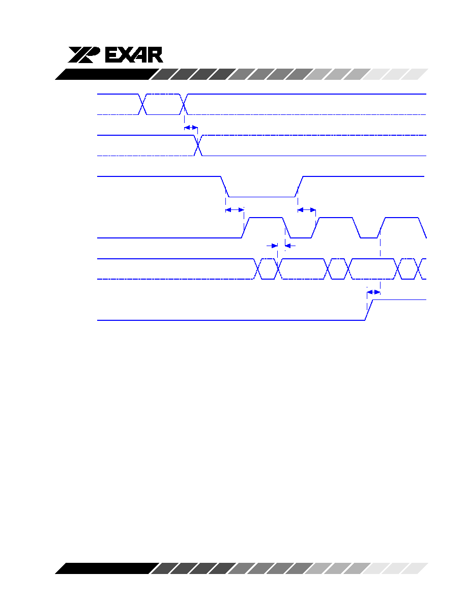
XR16C850
43
Rev. 1.20
-IOW
IOW
-RTS
-DTR
-CD
-CTS
-DSR
INT
-IOR
IOR
-RI
T17d
T18d
T18d
T19d
T18d
X450-MD-1
Active
Active
Change of state
Change of state
Active
Active
Active
Change of state
Change of state
Change of state
Active
Active
Modem Input/Output timing
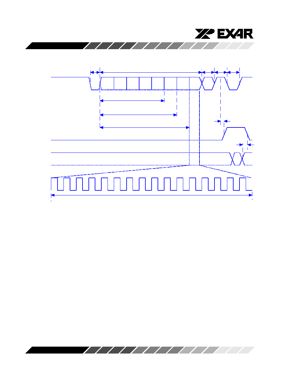
XR16C850
44
Rev. 1.20
STOP
BIT
PARITY
BIT
DATA BITS (5-8)
D0
D1
D2
D3
D4
D5
D6
D7
5 DATA BITS
6 DATA BITS
7 DATA BITS
START
BIT
RX
NEXT
DATA
START
BIT
INT
-IOR
IOR
T20d
T21d
16 BAUD RATE CLOCK
X450-RX-1
Active
Receive timing
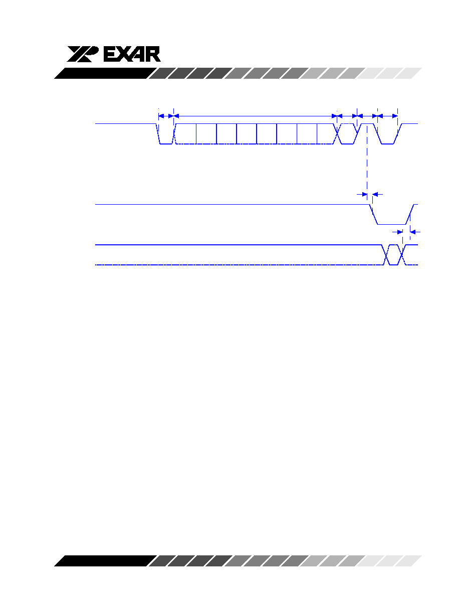
XR16C850
45
Rev. 1.20
STOP
BIT
PARITY
BIT
DATA BITS (5-8)
D0
D1
D2
D3
D4
D5
D6
D7
START
BIT
RX
NEXT
DATA
START
BIT
-RXRDY
-IOR
IOR
T25d
T26d
X550-RX-2
Active
Data
Ready
Active
Receive Ready timing in non FIFO mode

XR16C850
46
Rev. 1.20
STOP
BIT
PARITY
BIT
DATA BITS (5-8)
D0
D1
D2
D3
D4
D5
D6
D7
START
BIT
RX
First byte
that reaches
the trigger
level
-RXRDY
-IOR
IOR
T25d
T26d
X550-RX-3
Active
Data
Ready
Active
Receive Ready timing in FIFO mode

XR16C850
47
Rev. 1.20
STOP
BIT
PARITY
BIT
DATA BITS (5-8)
D0
D1
D2
D3
D4
D5
D6
D7
5 DATA BITS
6 DATA BITS
7 DATA BITS
START
BIT
TX
NEXT
DATA
START
BIT
INT
T22d
T24d
16 BAUD RATE CLOCK
X450-TX-1
-IOW
IOW
T23d
Active
Active
Tx Ready
Active
Transmit timing
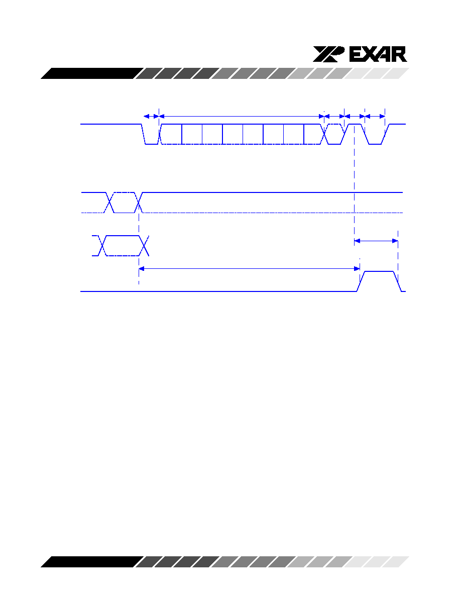
XR16C850
48
Rev. 1.20
STOP
BIT
PARITY
BIT
DATA BITS (5-8)
D0
D1
D2
D3
D4
D5
D6
D7
START
BIT
TX
NEXT
DATA
START
BIT
-TXRDY
T28d
X850-TX-2
-IOW
IOW
T27d
BYTE #128
FIFO
FULL
Transmit Ready timing in non FIFO mode
XR16C850
49
Rev. 1.20
STOP BIT
PARITY BIT
DATA BITS (5-8)
D0
D1
D2
D3
D4
D5
D6
D7
5 DATA BITS
6 DATA BITS
7 DATA BITS
START BIT
TX
-IOW
IOW
D0-D7
-TXRDY
BYTE #128
T28d
T27d
X850-TX-3
FIFO Full
Active
Transmit Ready timing in FIFO mode

XR16C850
50
Rev. 1.20
UART Frame
Data Bits
St
a
r
t
St
o
p
0
0
0
0
0
1
1
1
1
1
TX
IRTX
Bit Time
1/2 Bit Time
3/16 Bit Time
UART Frame
Data Bits
St
a
r
t
St
o
p
0
0
0
0
0
1
1
1
1
1
RX
IRRX
Bit Time
0-1 16x clock
delay
X650-IR-1
Infrared transmit timing
Infrared receive timing

XR16C850
51
Rev. 1.20

XR16C850
52
Rev. 1.20
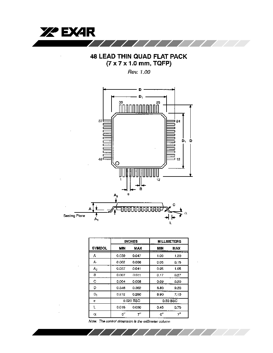
XR16C850
53
Rev. 1.20

XR16C850
54
Rev. 1.20

XR16C850
55
Rev. 1.20
NOTICE
EXAR Corporation reserves the right to make changes to the products contained in this publication in order to improve
design, performance or reliability. EXAR Corporation assumes no responsibility for the use of any circuits described
herein, conveys no license under any patent or other right, and makes no representation that the circuits are free of
patent infringement. Charts and schedules contained here in are only for illustration purposes and may vary depending
upon a user's specific application. While the information in this publication has been carefully checked; no
responsibility, however, is assumed for inaccuracies.
EXAR Corporation does not recommend the use of any of its products in life support applications where the failure
or malfunction of the product can reasonably be expected to cause failure of the life support system or to significantly
affect its safety or effectiveness. Products are not authorized for use in such applications unless EXAR Corporation
receives, in writing, assurances to its satisfaction that: (a) the risk of injury or damage has been minimized; (b) the
user assumes all such risks; (c) potential liability of EXAR Corporation is adequately protected under the
circumstances.
Copyright 1999 EXAR Corporation
Datasheet June 1999
Reproduction, in part or whole, without the prior written consent of EXAR Corporation is prohibited.