EXAR Corporation, 48720 Kato Road, Fremont, CA 94538
∑
(510) 668-7000
∑
FAX (510) 668-7017
XR16C872
Rev. 1.00
DUAL UART WITH 1284 PARALLEL PORT
AND PLUG-AND-PLAY CONTROLLER
FEATURES
∑
Plug and Play ISA Bus Specification Compliant
- Auto Configuration
- Direct Connection, Needing no External Buffers
- Resource Data in External 4K EEPROM
- Support 10-Interrupts, IRQ3-7, IRQ9-12, IRQ15
∑
Manual Configuration for standard COM1-COM-4
and LPT1-LPT2
∑
IEEE 1284 Compliant
- Bidirectional Host Port
- Level II Electrical Interface, Needing no
External Transceivers
- Standard Centronics/ECP/EPP Mode
- 16-byte FIFO in ECP mode
DESCRIPTION
August 2003
The XR16C872
1
(872) is a dual universal asynchronous receiver and transmitter (UART) with a 1284 bi-directional
parallel port and ISA Bus Plug-and-Play (PnP) interface. The PnP interface supports auto configuration for desktop
and embedded PC computers. The host bus interface can also be configured to manually support standard PC
addresses COM1-4 and LPT1-2. The parallel port is compatible to IEEE 1284 specification and supports Compatible
Centronics, Extended Capability (ECP) and Enhanced Parallel Port (EPP) protocols. The UARTs are software
compatible to industry standard 16C550 and include enhanced features of 128 bytes of transmit and receive FIFOs,
programmable transmit and receive FIFO trigger levels, transmit and receive FIFO counters, IrDA (Infrared Data
Association) encoder/decoder, automatic RTS/CTS hardware flow control with selectable hysteresis and automatic
software (Xon/Xoff) flow control. On board status registers provide interrupt priorities, receive data errors and modem
status. Each channel has a programmable baud rate generator to provide data rates up to 460.8Kbps. The bi-
directional parallel port can be configured as a general purpose input/output interface or connected to a printer or
portable storage devices. The 872 operates on a single +5V and +3.3 power supply. It is available in a small 100-
pin QFP package and offers commercial and industrial temperature ranges. The chip is fabricated in an advanced
CMOS process to reduce power consumption.
1
Covered by U.S. patent number 5,649,122 and patent pending.
2
Windows is a trademark of Microsoft Corp.
∑
Dual UART Software Compatible with 16C550
∑
128-byte of Transmit and Receive FIFOs to
Reduce CPU Bandwidth Requirement
∑
FIFO Counters in Transmitter and Receiver
∑
Automatic RTS/CTS Flow Control with Hysteresis
to Increase Data Throughput
∑
IrDA Infrared Pulse Shaping Encoder/decoder
for up to 115.2Kbps Data Rate
∑
Up to 460.8 Kbps Standard Serial Data Rate
∑
+5V and +3.3V Operation
∑
100-pin Quad Flat Package (14x20mm)
∑
Reference PC ISA Card Design Available
∑
Windows
2
95, 98 and NT4 Drivers Available
APPLICATIONS
∑
Multi-function PC/ISA Bus Card with RS-232/
RS-422/RS-485 Interface and Printer/parallel Port
∑
Embedded Systems
∑
Portable Infrared Wireless Systems
∑
High Speed Bidirectional Parallel Port
∑
High Speed Serial Ports
ORDERING INFORMATION
Part number
Package
Operating temperature
Device Status
XR16C872CQ
100-Lead QFP
0∞ C to + 70∞ C
Discontinued. No replacement available.
XR16C872IQ
100-Lead QFP
-40∞ C to + 85∞ C
Discontinued. No replacement available.
Visit Exar Web Site at www.exar.com
DISCONTINUED
XR16C872
2
Rev. 1.00
Visit Exar Web Site at www.exar.com
DISCONTINUED
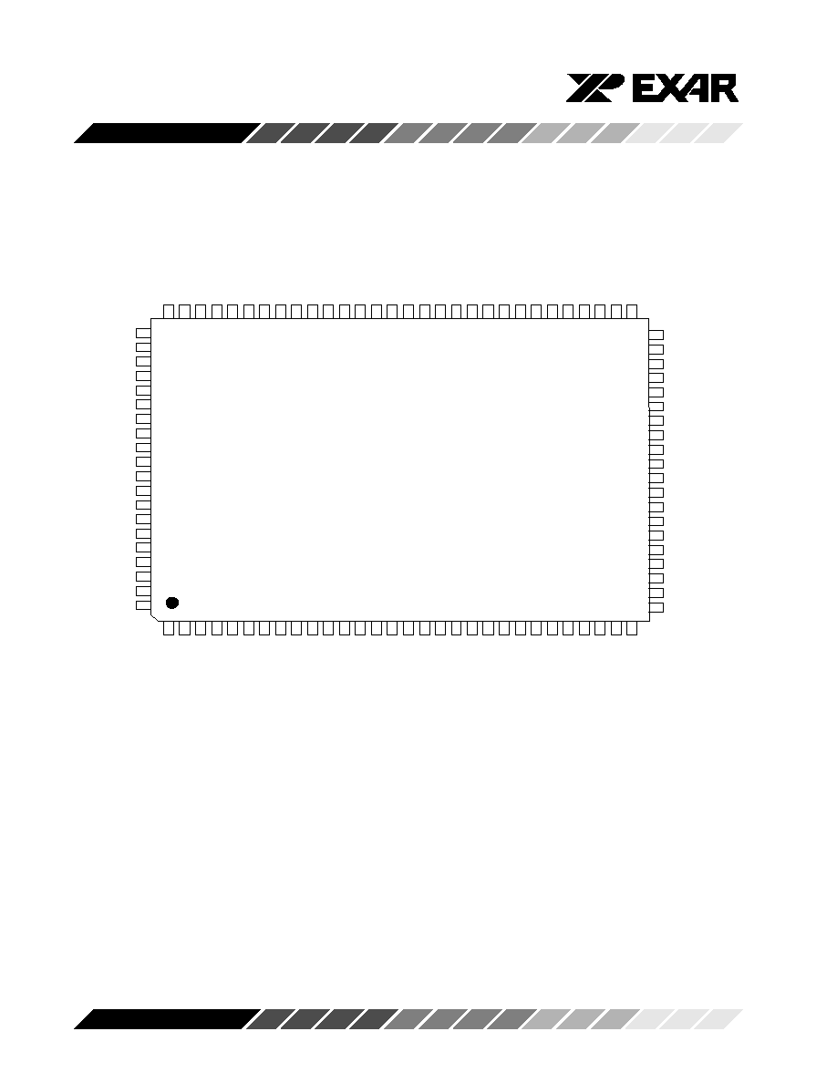
100 Pin PQFP (14X20x3 mm, 1.95 mm form)
ERR#
IOCHRDY
S E L C T I N #
A U T O F D #
S T R O B E #
S E L E C T
X R 1 6 C 8 7 2
80
79
78
77
76
75
74
73
72
71
70
69
68
67
66
65
64
63
62
61
60
59
58
57
56
55
54
53
52
51
DREQ1
DREQ3
DREQ5
GND
XTAL1
XTAL2
MAN#
EED
EECLK
EECS
RIA#
CDA#
DSRA#
CTSA#
RTSA#
DTRA#
TXA
RXA
VCC
GND
RIB#
CDB#
DSRB#
CTSB#
RTSB#
DTRB#
TXB
RXB
ACK#
1
2
3
4
5
6
7
8
9
10
11
12
13
14
15
16
17
18
19
20
21
22
23
24
25
26
27
28
29
30
RESET
A0
A1
A2
A3
A4
A5
A6
A7
A8
A9
A10
A11/LPT
A12/S4
A13/S3
GND
A14/S2
A15/S1
AEN
D7
D6
D5
D4
VCC
GND
D3
D2
D1
D0
P D I R
P D 7
P D 6
P D 5
V C C
G N D
P D 4
P D 3
P D 2
P D 1
P D 0
V C C
G N D
INIT#
P E
B U S Y
3 1
3 2
3 3
3 4
3 5
3 6
3 7
3 8
3 9
4 0
4 1
4 2
4 3
4 4
4 5
4 6
4 7
4 8
4 9
5 0
I O W #
I O R #
G N D
I R Q 9
I R Q 7
I R Q 6
I R Q 5
I R Q 4
I R Q 3
T C
V C C
I R Q 1 0
I R Q 1 2
I R Q 1 1
I R Q 1 5
D A C K 0 #
D A C K 1 #
D A C K 3 #
D A C K 5 #
D R E Q 0
1 0 0
9 9
9 8
9 7
9 6
9 5
9 4
9 3
9 2
9 1
9 0
8 9
8 8
8 7
8 6
8 5
8 4
8 3
8 2
8 1
Figure 1, Package Description (Top View)
XR16C872
3
Rev. 1.00
Visit Exar Web Site at www.exar.com
DISCONTINUED
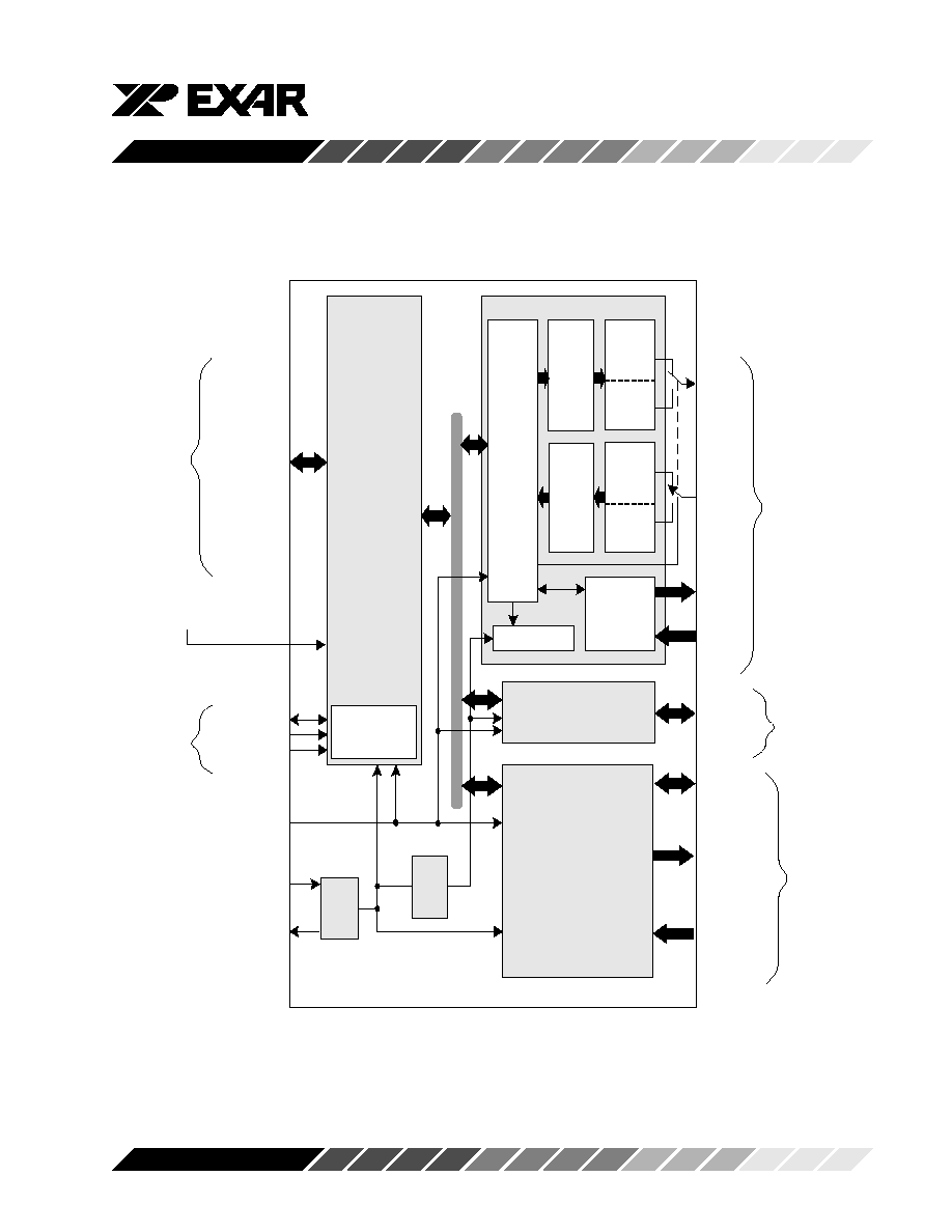
Figure 2, Funtional Block Diagram with Plug-and-Play Interface.
TXB,
RXB,
DTR#,
RTS#, etc.
To ISA Bus
To External
E E P R O M
To Serial Port A
Transceivers
To Parallel
Port Printer
D0-D7
A0-A15
A E N
IOR#
I O W #
I O C H R D Y
IRQ3-7,9-12,15
DREQ0,1,3,5
DACK0,1,3,5#
T C
E E D
E E C L K
E E C S
P D 0 - P D 7
INIT#
S T R O B E #
S E L C T I N #
A U T O F D #
P D I R
P E
S E L E C T
B U S Y
A C K #
E R R #
UART Channel B
(same as channel A block)
D T R A #
R T S A #
D S R A #
C T S A #
C D A #
RIA#
T X A
M o d e m
Interface
Transmit
FIFO
(128
bytes)
Transmit
Shift
Register
IrDA v1.0
Encoder
R X A
Receive
FIFO
(128
bytes)
Receive
Shift
Register
IrDA v1.0
Decoder
UART Channel A
X T A L 1
(22.1184 MHz)
X T A L 2
Baud Rate Gen.
1284 Bi-directional
Parallel Port Controller with
Level II Electrical Interface
ISA Bus
Plug-and-Play
Controller
Divide
by 3
Osc./
Buffer
7.3728 MHz
U A R T
Control
Registers
R E S E T
Internal Bus
EEPROM
Controller
To Serial Port B
Transceivers
M A N #
V C C
XR16C872
4
Rev. 1.00
Visit Exar Web Site at www.exar.com
DISCONTINUED
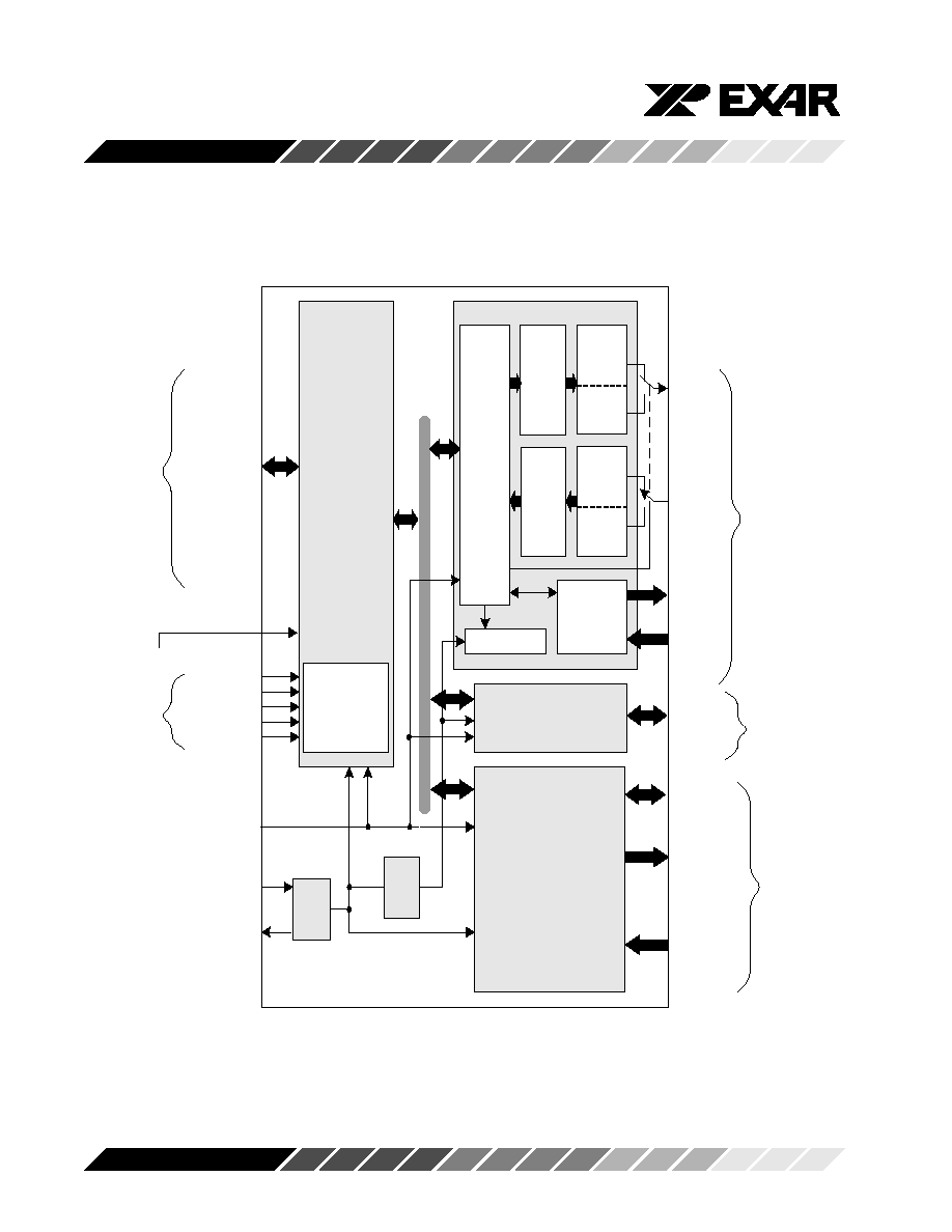
Figure 3, Funtional Block Diagram with Manual Configuration Interface.
TXB,
RXB,
DTR#,
RTS#, etc.
To ISA Bus
To Serial Port A
Transceivers
To Parallel
Printer Port
D0-D7
A0-A10
A E N
IOR#
I O W #
I O C H R D Y
IRQ3
IRQ4
IRQ5
IRQ7
D R E Q 3
D A C K 3 #
T C
S 1
S 2
S 3
S 4
S 5
P D 0 - P D 7
INIT#
S T R O B E #
S E L C T I N #
A U T O F D #
P D I R
P E
S E L E C T
B U S Y
A C K #
E R R #
UART Channel B
(same as channel A block)
D T R A #
R T S A #
D S R A #
C T S A #
C D A #
RIA#
T X A
M o d e m
Interface
Transmit
FIFO
(128
bytes)
Transmit
Shift
Register
IrDA v1.0
Encoder
R X A
Receive
FIFO
(128
bytes)
Receive
Shift
Register
IrDA v1.0
Decoder
UART Channel A
X T A L 1
(22.1184 MHz)
X T A L 2
Baud Rate Gen.
1284 Bi-directional
Parallel Port Controller with
Level II Electrical Interface
ISA Bus
Interface
Controller
Divide
by 3
Osc./
Buffer
7.3728 MHz
U A R T
Control
Registers
R E S E T
Internal Bus
To Serial Port B
Transceivers
Hardwired
or
Jumpers
Address
Decoder for
COM1-4 and
LP1-2
G N D
M A N #
XR16C872
5
Rev. 1.00
Visit Exar Web Site at www.exar.com
DISCONTINUED
PIN DESCRIPTION
Signal Type Definition. The following signal type definitions are from the 872 device point of view.
I
Standard input
O
Standard active output
OT24
Tri-state output
IOP14
Tri-state bi-directional input/output
IO24
Tri-state bi-directional input/output
HOST INTERFACE
A0-A15
2-15
I
ISA Bus Address. All 16 bits are used during PnP auto configuration
17,18
sequence with external EEPROM providing the resource data. In the
manual configuration mode A0-A10 are used for decoding COM1-4 and
LPT1-2 addresses. After auto or manual configuration, bits A0-A2 select
UART internal registers and A3-A10 are used to select UART A or B, or
the 1284 printer port.
D0-D7
30-21
IO24
ISA Data Bus. These are the eight three state data lines for transferring
data to or from the controlling CPU. D0 is the least significant bit and the
first data bit in a transmit or receive serial data stream.
AEN
19
I
Address Enable. Active high to validate A0-A15 address lines during Direct
Memory Access operation on the ISA bus. Connect to logic 0 when it is not used.
IOR#
99
I
Read Strobe. A logic 0 transition on this pin will request the contents of
an Internal register defined by address bits A0-A2 for either UART channels
A/B or A0-A1 for the printer port, be place onto D0-D7 data bus for a read
cycle by the CPU.
IOW#
100
I
Write Strobe. A logic 1 transition on this pin will transfer the data on the
data bus (D0-D7), as defined by either address bits A0-A2 for UART channels
A/B or A0-A1 for the printer port, into an internal register during a write cycle
from the CPU.
IRQ15
86
OT24
Interrupt Request Lines. These are three state active high interrupt lines to
IRQ12-10
87-89
controlling CPU when an interrupt request is generated by the UART
IRQ9
97
channel A/B or 1284 printer port.
IRQ3-7
92-96
DREQ5
78
OT24
DMA Request Channel 0,1,3 and 5. These are three state active high
DREQ3
79
outputs with internal weak pull down resistor. DMA request is used
DREQ1
80
by the 1284 parallel port during ECP and FIFO mode.
DREQ0
81
DACK5#
82
I
DMA Acknowledge Channel 0,1,3 and 5. These are active low inputs
DACK3#
83
and are used by the 1284 parallel port during ECP and FIFO mode.
DACK1#
84
DACK0#
85
Name
Pin #
Type
Pin Description