Exar
Corporation 48720 Kato Road, Fremont CA, 94538
�
(510) 668-7000
�
FAX (510) 668-7017
�
www.exar.com
��
��
��
��
XR16L2551
LOW VOLTAGE DUART WITH POWERSAVE
SEPTEMBER 2003
REV. 1.0.0
GENERAGENERAL DESCRIPTION
The XR16L2551 (L2551) is a low voltage dual
universal asynchronous receiver and transmitter
(UART) with 5 Volt tolerant inputs. The device
includes additional capability over the ST16C2550:
Intel and Motorola data bus interface selection,
hardware and software flow control, infrared encoder/
decoder, sleep mode and a PowerSave mode for
battery operation. The L2551's enhanced register set
is compatible to the ST16C2550 and XR16L2550. It
supports the Exar's enhanced features of 16 bytes of
TX and RX FIFOs and a complete modem interface.
Onboard registers provide the user with operational
status and data error tags. An internal loopback
capability allows onboard diagnostics. Independent
programmable baud rate generator is provided in
each channel to support data rates up to 3.125 Mbps.
N
OTE
:
1 Covered by U.S. Patent #5,649,122.
APPLICATIONS
�
Battery Operated Instruments
�
Data Port Adapters
�
Handheld Appliances
�
Radio Frequency Data Modems
�
Base Stations
�
USB Hubs
�
Industrial Automation Controls
FEATURES
�
2.25 to 5.5 Volt Operation
�
5 Volt Tolerant Inputs
�
Intel or Motorola Bus Interface Select (16/68#)
pin
�
Pin-to-pin compatible to XR16L2751CM
�
Two Independent UARTs
s
Up to 3.125 Mbps at 5V, 2 Mbps at 3.3V, and 1
Mbps at 2.5V with external clock input
s
Up to 1.5 Mbps at 5V, 1.25 Mbps at 3.3V and 1
Mbps at 2.5V with crystal clock input
s
16 bytes of Transmit and Receive FIFOs
s
Automatic RTS/CTS hardware flow control
s
Automatic Xon/Xoff software flow control
s
Wireless infrared encoder/decoder
s
Receive FIFO trigger levels select
s
Programmable character lengths (5, 6, 7 or 8)
with even, odd, forced or no parity
s
Full Modem Interface (CTS#, RTS#, DSR#,
DTR#, RI#, CD#) in the 48-TQFP package
�
Sleep Mode with PowerSave feature for battery
operation
�
Industrial Temperature range
�
Tiny 32-QFN, no lead package (5x5x0.9mm)
�
48-TQFP Package
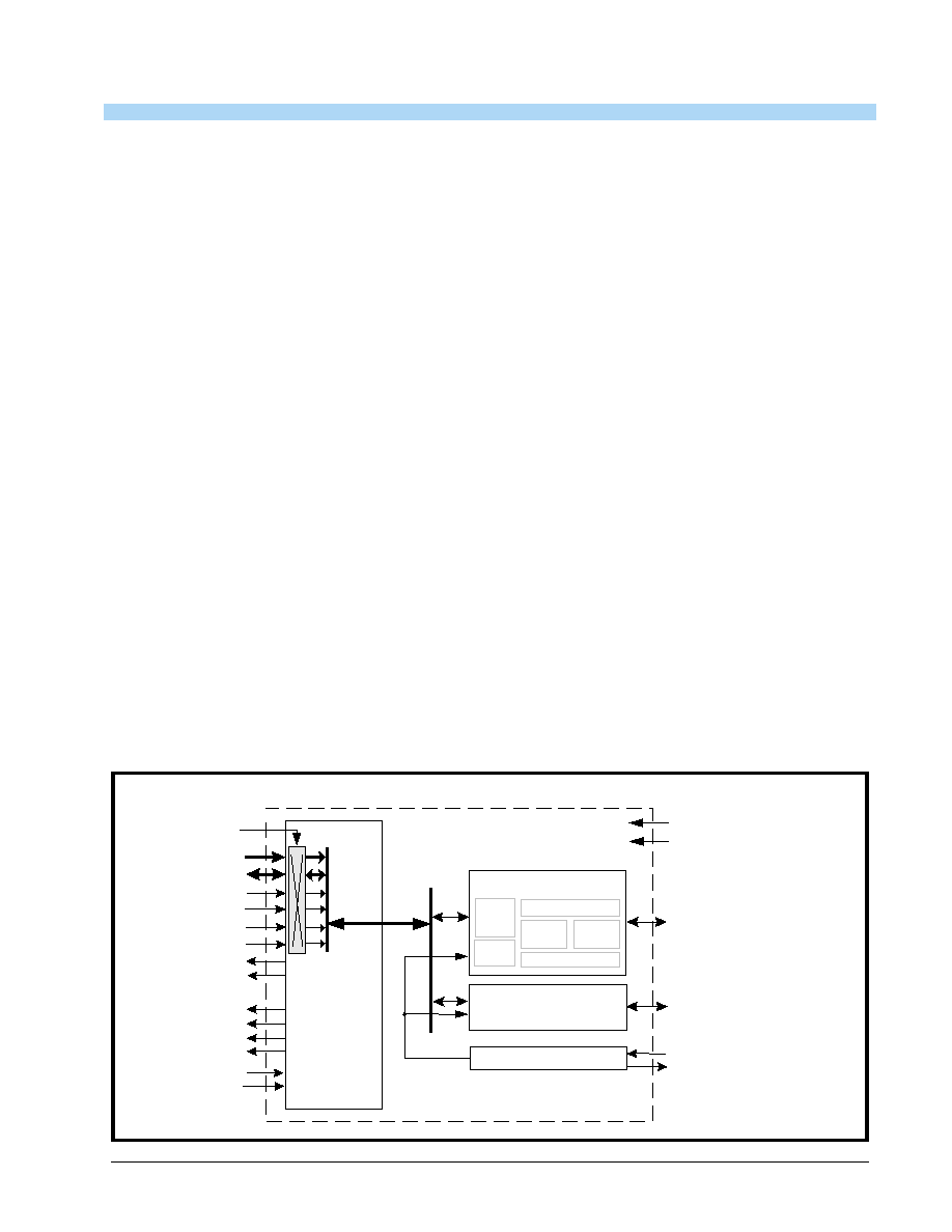
F
IGURE
1. XR16L2551 B
LOCK
D
IAGRAM
XTAL1
XTAL2
Crystal Osc/Buffer
TXA, RXA,
RTSA#, CTSA#,
( DTR#, DSR#
CD#, RIA#, OP2A# )
Intel or
Motorola
Data Bus
Interface
UART Channel A
16 Byte TX FIFO
16 Byte RX FIFO
BRG
IR
ENDEC
TX & RX
UART
Regs
2.25 to 5.5 Volt VCC
GND
*5 Volt Tolerant Inputs
2551BLK
UART Channel B
(same as Channel A)
A2:A0
D7:D0
CSA# (CS#)
16/68#
CSB# (A3)
INTA (IRQ#)
INTB (logic 0)
PwrSave
IOW# (R/W#)
IOR# (VCC)
Reset (Reset#)
TXRDYA#
TXRDYB#
RXRDYA#
RXRDYB#
TXB, RXB,
RTSB#, CTSB#,
( DTRB#, DSRB#
CDB#, RIB#, OP2B# )
XR16L2551
��
��
��
��
LOW VOLTAGE DUART WITH POWERSAVE
REV. 1.0.0
2
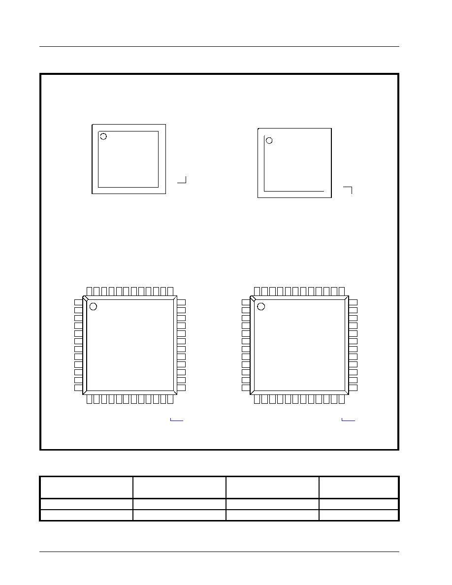
F
IGURE
2. P
IN
O
UT
A
SSIGNMENT
ORDERING INFORMATION
P
ART
N
UMBER
P
ACKAGE
O
PERATING
T
EMPERATURE
R
ANGE
D
EVICE
S
TATUS
XR16L2551IL
32-Lead QFN
-40�C to +85�C
Active
XR16L2551IM
48-Lead TQFP
-40�C to +85�C
Active
48
47
46
45
44
43
42
41
40
39
38
37
1
2
3
4
5
6
7
8
9
10
11
12
36
35
34
33
32
31
30
29
28
27
26
25
13
14
15
16
17
18
19
20
21
22
23
24
D5
D6
D7
RXB
RXA
TXRDYB#
TXA
TXB
OP2B#
CSA#
CSB#
PWRSAVE
XT
A
L
1
XT
A
L
2
IO
W
#
CD
B#
GND
RX
RD
YB
#
IO
R
#
DS
RB
#
RI
B#
RT
S
B
#
CT
S
B
#
16
/
6
8
#
RESET
DTRB#
DTRA#
RTSA#
OP2A#
RXRDYA#
INTA
INTB
A0
A1
A2
NC
D4
D3
D2
D1
D0
T
X
RDY
A#
VC
C
RI
A#
CD
A#
DS
RA
#
CT
S
A
#
XR16L2551
48-pin TQFP
in 16 (Intel) Mode
VCC
NC
48
47
46
45
44
43
42
41
40
39
38
37
1
2
3
4
5
6
7
8
9
10
11
12
36
35
34
33
32
31
30
29
28
27
26
25
13
14
15
16
17
18
19
20
21
22
23
24
D5
D6
D7
RXB
RXA
TXRDYB#
TXA
TXB
OP2B#
CS#
A3
PWRSAVE
XT
AL
1
XT
AL
2
IO
W
#
CDB
#
GND
RX
RDYB
#
VC
C
DS
RB#
RI
B
#
RT
S
B
#
CT
S
B
#
16
/68
#
RESET#
DTRB#
DTRA#
RTSA#
OP2A#
RXRDYA#
IRQ#
NC
A0
A1
A2
NC
D4
D3
D2
D1
D0
T
X
RDYA
#
VC
C
RI
A
#
CDA
#
DS
RA#
CT
S
A
#
NC
XR16L2551
48-pin TQFP in
68 (Motorola) Mode)
GND
32
31
30
29
1
2
3
4
5
6
7
8
24
23
22
21
20
19
11
12
13
14
15
16
9
10
D5
D6
D7
RXB
RXA
TXA
TXB
CSA#
CSB#
X
T
AL
1
X
T
AL
2
IO
W
#
GND
IO
R
#
RT
S
B
#
CT
S
B
#
RESET
RTSA#
INTA
INTB
A0
A1
A2
D4
D3
D2
D1
D0
VC
C
CT
S
A
#
XR16L2551
32-pin QFN in
16 (Intel) Mode
28
27
26
25
18
17
P
W
RS
AV
E
16/68#
VCC
32
31
30
29
1
2
3
4
5
6
7
8
24
23
22
21
20
19
11
12
13
14
15
16
9
10
D5
D6
D7
RXB
RXA
TXA
TXB
CS#
A3 (CSB#)
X
T
AL
1
X
T
AL
2
R
/W#
GND
VC
C
(
I
O
R
#
)
RT
S
B
#
CT
S
B
#
RESET# (Reset)
RTSA#
IRQ#
NC (INTB)
A0
A1
A2
D4
D3
D2
D1
D0
VC
C
CT
S
A
#
XR16L2551
32-pin QFN in
68 (Motorola) Mode
28
27
26
25
18
17
P
W
RS
AV
E
16/68#
GND
��
��
��
��
XR16L2551
REV. 1.0.0
LOW VOLTAGE DUART WITH POWERSAVE
3
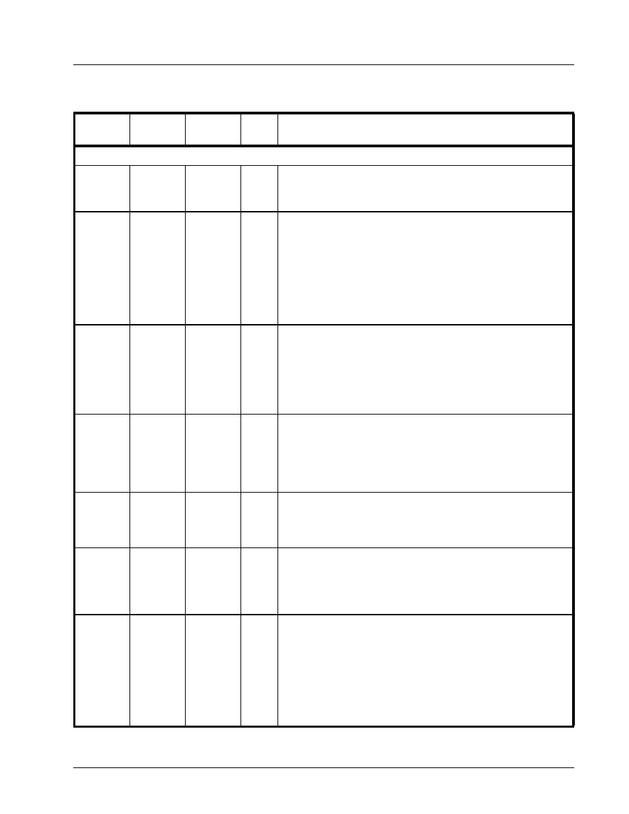
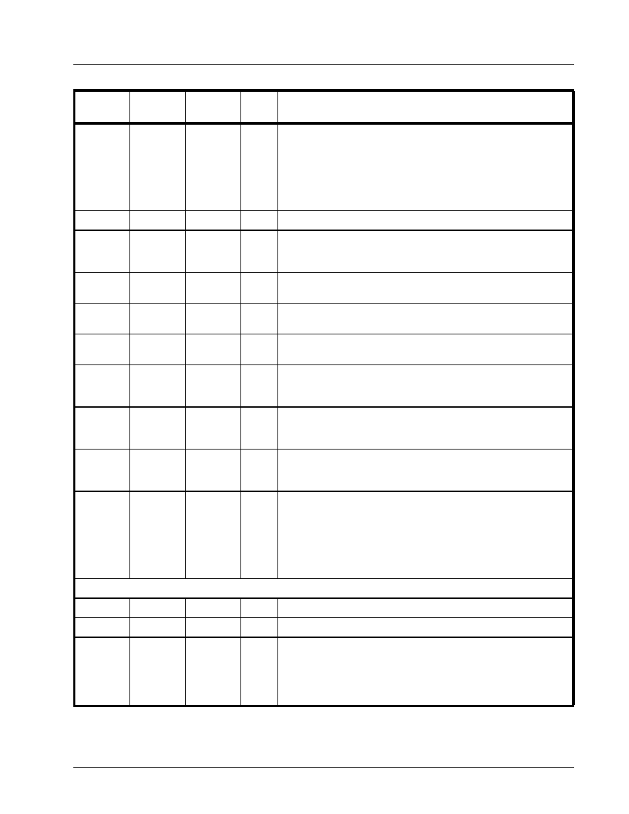
PIN DESCRIPTIONS
Pin Description
N
AME
32-QFN
P
IN
#
48-TQFP
P
IN
#
T
YPE
D
ESCRIPTION
DATA BUS INTERFACE
A2
A1
A0
18
19
20
26
27
28
I
Address data lines [2:0]. These 3 address lines select one of the inter-
nal registers in UART channel A/B during a data bus transaction.
D7
D6
D5
D4
D3
D2
D1
D0
2
1
32
31
30
29
28
27
3
2
1
48
47
46
45
44
IO
Data bus lines [7:0] (bidirectional).
IOR#
(VCC)
14
19
I
When 16/68# pin is at logic 1, the Intel bus interface is selected and this
input becomes read strobe (active low). The falling edge instigates an
internal read cycle and retrieves the data byte from an internal register
pointed by the address lines [A2:A0], puts the data byte on the data bus
to allow the host processor to read it on the rising edge.
When 16/68# pin is at logic 0, the Motorola bus interface is selected
and this input is not used and should be connected to VCC.
IOW#
(R/W#)
12
15
I
When 16/68# pin is at logic 1, it selects Intel bus interface and this input
becomes write strobe (active low). The falling edge instigates the inter-
nal write cycle and the rising edge transfers the data byte on the data
bus to an internal register pointed by the address lines.
When 16/68# pin is at logic 0, the Motorola bus interface is selected
and this input becomes read (logic 1) and write (logic 0) signal.
CSA#
(CS#)
7
10
I
When 16/68# pin is at logic 1, this input is chip select A (active low) to
enable channel A in the device.
When 16/68# pin is at logic 0, this input becomes the chip select (active
low) for the Motorola bus interface.
CSB#
(A3)
8
11
I
When 16/68# pin is at logic 1, this input is chip select B (active low) to
enable channel B in the device.
When 16/68# pin is at logic 0, this input becomes address line A3
which is used for channel selection in the Motorola bus interface. Input
logic 0 selects channel A and logic 1 selects channel B.
INTA
(IRQ#)
22
30
O
When 16/68# pin is at logic 1 for Intel bus interface, this output
becomes channel A interrupt output. The output state is defined by the
user through the software setting of MCR[3]. INTA is set to the active
mode and OP2A# output to a logic 0 when MCR[3] is set to a logic 1.
INTA is set to the three state mode and OP2A# to a logic 1 when
MCR[3] is set to a logic 0. See MCR[3].
When 16/68# pin is at logic 0 for Motorola bus interface, this output
becomes device interrupt output (active low, open drain). An external
pull-up resistor is required for proper operation.
XR16L2551
��
��
��
��
LOW VOLTAGE DUART WITH POWERSAVE
REV. 1.0.0
4
INTB
(NC)
21
29
O
When 16/68# pin is at logic 1 for Intel bus interface, this output
becomes channel B interrupt output. The output state is defined by the
user and through the software setting of MCR[3]. INTB is set to the
active mode and OP2B# output to a logic 0 when MCR[3] is set to a
logic 1. INTB is set to the three state mode and OP2B# to a logic 1
when MCR[3] is set to a logic 0. See MCR[3].
When 16/68# pin is at logic 0 for Motorola bus interface, this output is
not used and will stay at logic zero level. Leave this output uncon-
nected.
TXRDYA#
-
43
O
UART channel A Transmitter Ready (active low). The output
provides the TX FIFO/THR status for transmit channel A. If it is
not used, leave it unconnected.
RXRDYA#
-
31
O
UART channel A Receiver Ready (active low). This output provides the
RX FIFO/RHR status for receive channel A. If it is not used, leave it
unconnected.
TXRDYB#
-
6
O
UART channel B Transmitter Ready (active low). The output provides
the TX FIFO/THR status for transmit channel B. If it is not used, leave it
unconnected.
RXRDYB#
-
18
O
UART channel B Receiver Ready (active low). This output provides the
RX FIFO/RHR status for receive channel B. If it is not used, leave it
unconnected.
MODEM OR SERIAL I/O INTERFACE
TXA
5
7
O
UART channel A Transmit Data. If it is not used, leave it unconnected.
RXA
4
5
I
UART channel A Receive Data. Normal receive data input must idle at
logic 1 condition. If it is not used, tie it to VCC or pull it high via a 100k
ohm resistor.
RTSA#
23
33
O
UART channel A Request-to-Send (active low) or general purpose out-
put. If it is not used, leave it unconnected.
CTSA#
25
38
I
UART channel A Clear-to-Send (active low) or general purpose input.
This input should be connected to VCC when not used.
DTRA#
-
34
O
UART channel A Data-Terminal-Ready (active low) or general purpose
output. If it is not used, leave it unconnected.
DSRA#
-
39
I
UART channel A Data-Set-Ready (active low) or general purpose input.
This input should be connected to VCC when not used. This input has
no effect on the UART.
CDA#
-
40
I
UART channel A Carrier-Detect (active low) or general purpose input.
This input should be connected to VCC when not used. This input has
no effect on the UART.
RIA#
-
41
I
UART channel A Ring-Indicator (active low) or general purpose input.
This input should be connected to VCC when not used. This input has
no effect on the UART.
Pin Description
N
AME
32-QFN
P
IN
#
48-TQFP
P
IN
#
T
YPE
D
ESCRIPTION
��
��
��
��
XR16L2551
REV. 1.0.0
LOW VOLTAGE DUART WITH POWERSAVE
5
OP2A#
-
32
O
Output Port 2 Channel A - The output state is defined by the user and
through the software setting of MCR[3]. INTA is set to the active mode
and OP2A# output to a logic 0 when MCR[3] is set to a logic 1. INTA is
set to the three state mode and OP2A# to a logic 1 when MCR[3] is set
to a logic 0. This output should not be used as a general output else it
will disturb the INTA output functionality. If it is not used at all, leave it
unconnected.
TXB
6
8
O
UART channel B Transmit Data. If it is not used, leave it unconnected.
RXB
3
4
I
UART channel B Receive Data. Normal receive data input must idle at
logic 1 condition. If it is not used, tie it to VCC or pull it high via a 100k
ohm resistor.
RTSB#
15
22
O
UART channel B Request-to-Send (active low) or general purpose out-
put. If it is not used, leave it unconnected.
CTSB#
16
23
I
UART channel B Clear-to-Send (active low) or general purpose input.
This input should be connected to VCC when not used.
DTRB#
-
35
O
UART channel B Data-Terminal-Ready (active low) or general purpose
output. If it is not used, leave it unconnected.
DSRB#
-
20
I
UART channel B Data-Set-Ready (active low) or general purpose input.
This input should be connected to VCC when not used. This input has
no effect on the UART.
CDB#
-
16
I
UART channel B Carrier-Detect (active low) or general purpose input.
This input should be connected to VCC when not used. This input has
no effect on the UART.
RIB#
-
21
I
UART channel B Ring-Indicator (active low) or general purpose input.
This input should be connected to VCC when not used. This input has
no effect on the UART.
OP2B#
-
9
O
Output Port 2 Channel B - The output state is defined by the user and
through the software setting of MCR[3]. INTB is set to the active mode
and OP2B# output to a logic 0 when MCR[3] is set to a logic 1. INTB is
set to the three state mode and OP2B# to a logic 1 when MCR[3] is set
to a logic 0. This output should not be used as a general output else it
will disturb the INTB output functionality. If it is not used, leave it uncon-
nected.
ANCILLARY SIGNALS
XTAL1
10
13
I
Crystal or external clock input.
XTAL2
11
14
O
Crystal or buffered clock output.
16/68#
17
24
I
Intel or Motorola Bus Select.
When 16/68# pin is at logic 1, 16 or Intel Mode, the device will operate
in the Intel bus type of interface.
When 16/68# pin is at logic 0, 68 or Motorola mode, the device will
operate in the Motorola bus type of interface.
Pin Description
N
AME
32-QFN
P
IN
#
48-TQFP
P
IN
#
T
YPE
D
ESCRIPTION