Äîêóìåíòàöèÿ è îïèñàíèÿ www.docs.chipfind.ru
Exar
Corporation 48720 Kato Road, Fremont CA, 94538
·
(510) 668-7000
·
FAX (510) 668-7017
·
www.exar.com
xr
XR16L2552
2.25V TO 5.5V DUART WITH 16-BYTE FIFO
MAY 2005
REV. 1.1.1
GENERAL DESCRIPTION
The XR16L2552 (L2552) is a dual universal
asynchronous receiver and transmitter (UART) with 5
volt tolerant inputs. The XR16L2552 is an improved
version of the ST16C2552 UART with lower operating
voltages and 5 volt tolerant inputs. The L2552
provides enhanced UART functions with 16 byte TX
and RX FIFOs, automatic hardware (RTS/CTS) and
software (Xon/Xoff) flow control, and a complete
modem control interface. Onboard status registers
provide the user with error indications and
operational status. Indepedendent programmable
baud rate generators are provided to select transmit
and receive clock rates up to 3.125Mbps. An internal
loop-back capability allows onboard diagnostics. The
L2552 provides block mode data transfers (DMA)
through FIFO controls. DMA transfer monitoring is
provided through the signals TXRDY# and RXRDY#.
An Alternate Function Register provides the user with
the ability to write the control registers for both UARTs
concurrently and selection of the Multi-Function
output (Baudout#, OP2#, or RXRDY#).
N
OTE
:
1 Covered by U.S. Patent #5,649,122.
APPLICATIONS
·
Portable Appliances
·
Telecommunication Network Routers
·
Ethernet Network Routers
·
Cellular Data Devices
·
Factory Automation and Process Controls
FEATURES
·
2.25 to 5.5 Volt Operation
·
5 Volt Tolerant Inputs
·
Pin-to-pin and functionally compatible to National
PC16552
·
Pin-to-pin Compatible to Exar's ST16C2552,
XR16L2752 and XR16C2852 in the 44-PLCC
·
2 Independent UART Channels
Up to 3.125Mbps with external clock of 50 MHz
Register Set Compatible to 16C550
16 byte Transmit FIFO to reduce the bandwidth
requirement of the external CPU
16 byte Receive FIFO with error tags to reduce
the bandwidth requirement of the external CPU
4 selectable RX FIFO Trigger Levels
Automatic RTS/CTS hardware flow control
Automatic XonXoff software flow control
Wireless infrared encoder/decoder
Full Modem Interface (CTS#, RTS#, DSR#,
DTR#, RI#, CD#)
Programmable character lengths (5, 6, 7, 8)
with even, odd, or no parity
Multi-Function output allows more package
functions with fewer I/O pins
·
Concurrent write to Channels A and B
·
Crystal oscillator or external clock input
·
48-TQFP (7x7x1.0 mm) and 44-PLCC packages
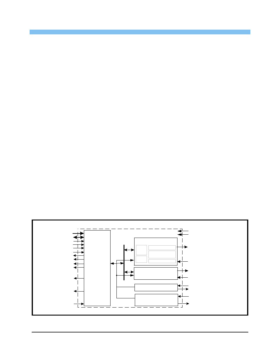
F
IGURE
1. XR16L2552 B
LOCK
D
IAGRAM
MFA#
(OP2A#,
BAUDOUTA#, or
RXRDYA#)
MFB#
(OP2B#,
BAUDOUTB#, or
RXRDYB#)
XTAL1
XTAL2
Crystal Osc/Buffer
TXA
8-bit Data
Bus
Interface
UART Channel A
16 Byte TX FIFO
16 Byte RX FIFO
BRG
TX & RX
UART
Regs
2.25 to 5.5 Volt VCC
GND
2552BLK
UART Channel B
(same as Channel A)
A2:A0
D7:D0
CS#
CHSEL
INTA
INTB
IOW#
IOR#
Reset
TXRDY# A/B
RXRDY# A/B
(48-TQFP Only)
CTS#A/B, RI#A/B,
CD#A/B, DSR#A/B
RXA
Modem Control Logic
DTR#A/B, RTS#A/B
TXB
RXB
* 5 Volt Tolerant Inputs
XR16L2552
xr
2.25V TO 5.5V DUART WITH 16-BYTE FIFO
REV. 1.1.1
2
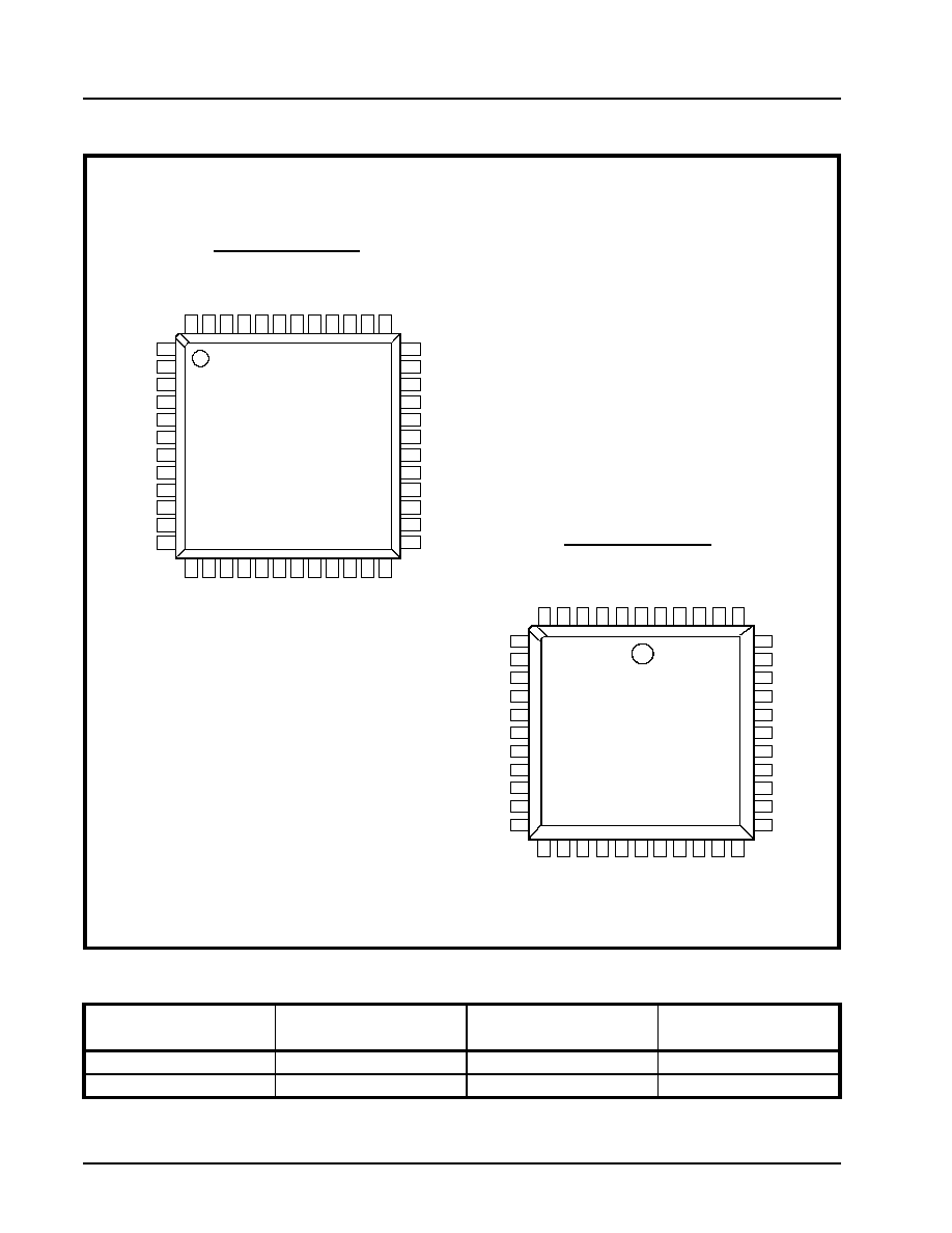
F
IGURE
2. P
IN
O
UT
A
SSIGNMENTS
ORDERING INFORMATION
P
ART
N
UMBER
P
ACKAGE
O
PERATING
T
EMPERATURE
R
ANGE
D
EVICE
S
TATUS
XR16L2552IM
48-Lead TQFP
-40°C to +85°C
Active
XR16L2552IJ
44-Lead PLCC
-40°C to +85°C
Active
6
5
4
3
2
1
44
43
42
41
40
7
8
9
10
11
12
13
14
15
16
17
39
38
37
36
35
34
33
32
31
30
29
18
19
20
21
22
23
24
25
26
27
28
D5
D6
D7
A0
XTAL1
GND
XTAL2
A1
A2
CHSEL
INTB
RXA
TXA
DTRA#
RTSA#
MFA#
INTA
VCC
TXRDYB#
RIB#
CDB#
DSRB#
CS
#
MF
B#
IO
W
#
RE
SE
T
GND
RT
SB
#
IO
R
#
RX
B
TX
B
DT
RB
#
CT
S
B
#
D4
D3
D2
D1
D0
TX
RD
YA
#
VC
C
RI
A#
CD
A#
DS
RA
#
CT
SA
#
XR16L2552
44-pin PLCC
48
47
46
45
44
43
42
41
40
39
38
37
1
2
3
4
5
6
7
8
9
10
11
12
36
35
34
33
32
31
30
29
28
27
26
25
13
14
15
16
17
18
19
20
21
22
23
24
D5
D6
D7
A0
XTAL1
GND
XTAL2
A1
A2
CHSEL
INTB
CS
#
MF
B#
IO
W
#
RE
SE
T
GN
D
RTS
B
#
NC
IO
R#
RX
B
TX
B
DTR
B
#
CTS
B
#
RXA
TXA
DTRA#
RTSA#
MFA#
RXRDYA#
INTA
VCC
TXRDYB#
RIB#
CDB#
DSRB#
D4
D3
D2
D1
D0
T
X
RD
YA
#
VC
C
RI
A#
CD
A#
DSR
A
#
CTS
A
#
NC
XR16L2552
48-pin TQFP
RXRDYB#
48-TQFP PACKAGE
44-PLCC PACKAGE
xr
XR16L2552
REV. 1.1.1
2.25V TO 5.5V DUART WITH 16-BYTE FIFO
3
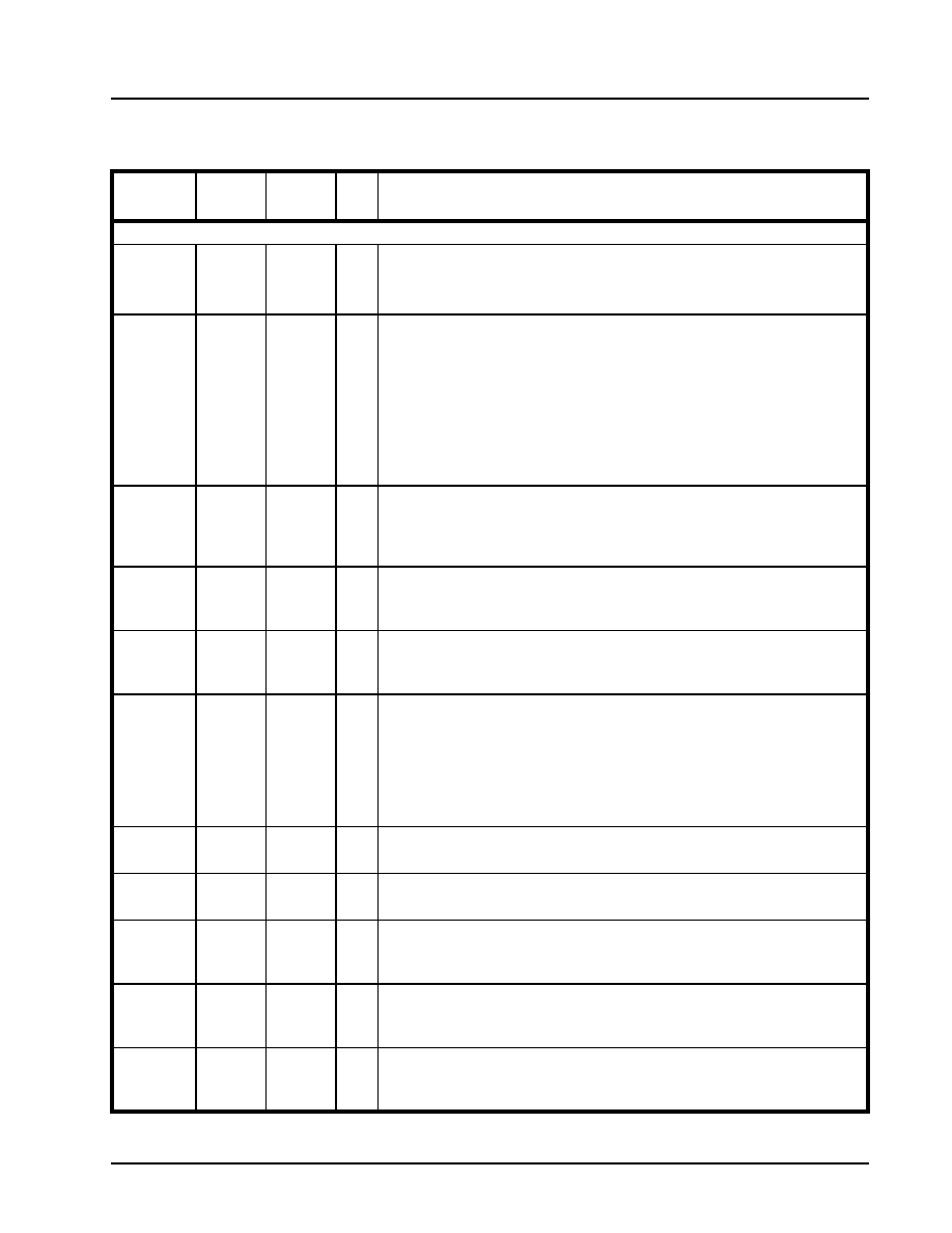
PIN DESCRIPTIONS
Pin Description
N
AME
48-TQFP
P
IN
#
44-PLCC
P
IN
#
T
YPE
D
ESCRIPTION
DATA BUS INTERFACE
A2
A1
A0
10
9
4
15
14
10
I
Address data lines [2:0]. These 3 address lines select one of the internal reg-
isters in UART channel A/B during a data bus transaction.
D7
D6
D5
D4
D3
D2
D1
D0
3
2
1
48
47
46
45
44
9
8
7
6
5
4
3
2
I/O
Data bus lines [7:0] (bidirectional).
IOR#
20
24
I
Input/Output Read Strobe (active low). The falling edge instigates an internal
read cycle and retrieves the data byte from an internal register pointed to by
the address lines [A2:A0]. The data byte is placed on the data bus to allow the
host processor to read it on the rising edge.
IOW#
15
20
I
Input/Output Write Strobe (active low). The falling edge instigates an internal
write cycle and the rising edge transfers the data byte on the data bus to an
internal register pointed by the address lines.
CS#
13
18
I
UART chip select (active low). This function selects channel A or B in accor-
dance with the logical state of the CHSEL pin. This allows data to be trans-
ferred between the user CPU and the L2552.
CHSEL
11
16
I
Channel Select - UART channel A or B is selected by the logical state of this
pin when the CS# pin is a logic 0. A logic 0 on the CHSEL selects the UART
channel B while a logic 1 selects UART channel A. Normally, CHSEL could
just be an address line from the user CPU such as A3. Bit-0 of the Alternate
Function Register (AFR) can temporarily override CHSEL function, allowing
the user to write to both channel register simultaneously with one write cycle
when CS# is low. It is especially useful during the initialization routine.
INTA
30
34
O
UART channel A Interrupt output (active high). A logic high indicates channel
A is requesting for service.
INTB
12
17
O
UART channel B Interrupt output (active high). A logic high indicates channel
B is requesting for service.
TXRDYA#
43
1
O
UART channel A Transmitter Ready (active low). The output provides the TX
FIFO/THR status for transmit channel A. If it is not used, leave it uncon-
nected.
RXRDYA#
31
-
O
UART channel A Receiver Ready (active low). This output provides the RX
FIFO/RHR status for receive channel A. This pin is only available on the 48-
pin TQFP package. If it is not used, leave it unconnected.
TXRDYB#
28
32
O
UART channel B Transmitter Ready (active low). The output provides the TX
FIFO/THR status for transmit channel B. If it is not used, leave it uncon-
nected.
XR16L2552
xr
2.25V TO 5.5V DUART WITH 16-BYTE FIFO
REV. 1.1.1
4
RXRDYB#
8
-
O
UART channel B Receiver Ready (active low). This output provides the RX
FIFO/RHR status for receive channel B. This pin is only available on the 48-
pin TQFP package. If it is not used, leave it unconnected.
MODEM OR SERIAL I/O INTERFACE
TXA
35
38
O
UART channel A Transmit Data. If it is not used, leave it unconnected.
RXA
36
39
I
UART channel A Receive Data. Normal receive data input must idle at logic 1
condition. If it is not used, tie it to VCC or pull it high via a 100k ohm resistor.
RTSA#
33
36
O
UART channel A Request-to-Send (active low) or general purpose output.
This output must be asserted prior to using auto RTS flow control, see EFR[6],
MCR[1] and IER[6]. If it is not used, leave it unconnected.
CTSA#
38
40
I
UART channel A Clear-to-Send (active low) or general purpose input. It can
be used for auto CTS flow control, see EFR[7] and IER[7]. This input should
be connected to VCC when not used.
DTRA#
34
37
O
UART channel A Data-Terminal-Ready (active low) or general purpose output.
If it is not used, leave it unconnected.
DSRA#
39
41
I
UART channel A Data-Set-Ready (active low) or general purpose input. This
input should be connected to VCC when not used. This input has no effect on
the UART.
CDA#
40
42
I
UART channel A Carrier-Detect (active low) or general purpose input. This
input should be connected to VCC when not used. This input has no effect on
the UART.
RIA#
41
43
I
UART channel A Ring-Indicator (active low) or general purpose input. This
input should be connected to VCC when not used. This input has no effect on
the UART.
TXB
22
26
O
UART channel B Transmit Data. If it is not used, leave it unconnected.
RXB
21
25
I
UART channel B Receive Data. Normal receive data input must idle at logic 1
condition. If it is not used, tie it to VCC or pull it high via a 100k ohm resistor.
RTSB#
18
23
O
UART channel B Request-to-Send (active low) or general purpose output.
This output must be asserted prior to using auto RTS flow control, see EFR[6],
MCR[1] and IER[6]. If it is not used, leave it unconnected.
CTSB#
24
28
I
UART channel B Clear-to-Send (active low) or general purpose input. It can
be used for auto CTS flow control, see EFR[7] and IER[7]. This input should
be connected to VCC when not used.
DTRB#
23
27
O
UART channel B Data-Terminal-Ready (active low) or general purpose output.
If it is not used, leave it unconnected.
DSRB#
25
29
I
UART channel B Data-Set-Ready (active low) or general purpose input. This
input should be connected to VCC when not used. This input has no effect on
the UART.
CDB#
26
30
I
UART channel B Carrier-Detect (active low) or general purpose input. This
input should be connected to VCC when not used. This input has no effect on
the UART.
Pin Description
N
AME
48-TQFP
P
IN
#
44-PLCC
P
IN
#
T
YPE
D
ESCRIPTION
xr
XR16L2552
REV. 1.1.1
2.25V TO 5.5V DUART WITH 16-BYTE FIFO
5
RIB#
27
31
I
UART channel B Ring-Indicator (active low) or general purpose input. This
input should be connected to VCC when not used. This input has no effect on
the UART.
MFA#
32
35
O
Multi-Function Output Channel A. This output pin can function as the OP2A#,
BAUDOUTA#, or RXRDYA# pin. One of these output signal functions can be
selected by the user programmable bits 1-2 of the Alternate Function Register
(AFR). These signal functions are described as follows:
1) OP2A# - When OP2A# (active low) is selected, the MF# pin is a logic 0
when MCR bit-3 is set to a logic 1 (see MCR bit-3). MCR bit-3 defaults to a
logic 1 condition after a reset or power-up.
2) BAUDOUTA# - When BAUDOUTA# function is selected, the 16X Baud rate
clock output is available at this pin.
3) RXRDYA# - RXRDYA# (active low) is intended for monitoring DMA data
transfers. If using the 48-TQFP package, this output is already available at pin
31.
If it is not used, leave it unconnected.
MFB#
14
19
O
Multi-Function Output ChannelB. This output pin can function as the OP2B#,
BAUDOUTB#, or RXRDYB# pin. One of these output signal functions can be
selected by the user programmable bits 1-2 of the Alternate Function Register
(AFR). These signal functions are described as follows:
1) OP2B# - When OP2B# (active low) is selected, the MF# pin is a logic 0
when MCR bit-3 is set to a logic 1 (see MCR bit-3). MCR bit-3 defaults to a
logic 1 condition after a reset or power-up.
2) BAUDOUTB# - When BAUDOUTB# function is selected, the 16X Baud rate
clock output is available at this pin.
3) RXRDYB# - RXRDYB# (active low) is intended for monitoring DMA data
transfers. If using the 48-TQFP package, this output is already available at pin
8.
If it is not used, leave it unconnected.
ANCILLARY SIGNALS
XTAL1
5
11
I
Crystal or external clock input.
XTAL2
7
13
O
Crystal or buffered clock output.
RESET
16
21
I
Reset (active high) - A longer than 40 ns logic 1 pulse on this pin will reset the
internal registers and all outputs. The UART transmitter output will be held at
logic 1, the receiver input will be ignored and outputs are reset during reset
period (see External Reset Conditions).
VCC
29, 42
44, 33
Pwr 2.25V to 5.5V power supply. All input pins are 5V tolerant.
GND
6, 17
22, 12
Pwr Power supply common, ground.
Pin Description
N
AME
48-TQFP
P
IN
#
44-PLCC
P
IN
#
T
YPE
D
ESCRIPTION
Document Outline