Äîêóìåíòàöèÿ è îïèñàíèÿ www.docs.chipfind.ru
Exar
Corporation 48720 Kato Road, Fremont CA, 94538
·
(510) 668-7000
·
FAX (510) 668-7017
·
www.exar.com
áç
áç
áç
áç
XR16L784
HIGH PERFORMANCE 2.97V TO 5.5V QUAD UART
JUNE 2004
REV. 1.2.0
GENERAL DESCRIPTION
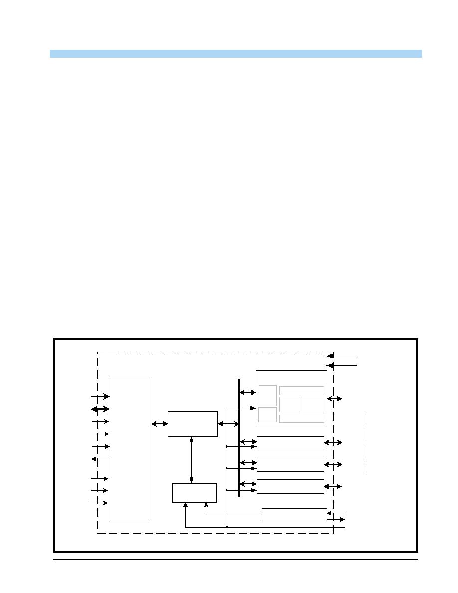
The XR16L784
1
(784) is a quad Universal
Asynchronous Receiver and Transmitter (UART). The
device is designed for high bandwidth requirement in
communication systems. The global interrupt source
register provides a complete interrupt status
indication for all 4 channels to speed up interrupt
parsing. Each UART has its own 16C550 compatible
set of configuration registers, transmit and receive
FIFOs of 64 bytes, fully programmable transmit and
receive FIFO level triggers, transmit and receive
FIFO level counters, automatic RTS/CTS or DTR/
DSR hardware flow control with programmable
hysteresis, automatic software (Xon/Xoff) flow
control, IrDA (Infrared Data Association) encoder/
decoder, and a 16-bit general purpose timer/counter.
N
OTE
:
1 Covered by U.S. Patents #5,649,122 and #5,949,787
APPLICATIONS
·
Remote Access Servers
·
Ethernet Network to Serial Ports
·
Network Management
·
Factory Automation and Process Control
·
Point-of-Sale Systems
·
Multi-port RS-232/RS-422/RS-485 Cards
FEATURES
·
2.97V to 5.5V operation with 5V Tolerant Inputs
·
8-bit Intel or Motorola Data Bus Interface
·
Single Open Drain Interrupt output for all 4 channels
·
Global Interrupt Source Registers for all channels
·
5G (Fifth Generation) "Flat" Register Set
·
Each UART is Independently Controlled with:
·
16C550 Compatible Registers
·
64-byte Transmit and Receive FIFOs
·
Transmit and Receive FIFO Level Counters
·
Programmable TX and RX FIFO Trigger Levels
·
Automatic RTS/CTS or DTR/DSR Flow Control
·
Selectable RTS Flow Control Hysteresis
·
Automatic Xon/Xoff Software Flow Control
·
Automatic RS485 Half-duplex Control Output with
16 Selectable Turn-around Delay
·
Infrared (IrDA 1.1) Data Encoder/Decoder
·
Programmable Data Rate with Prescaler
·
Up to 3.12 (16x) and 6.25 (8x) Mbps Data Rate
·
A General Purpose 16-bit Timer/Counter
·
Sleep Mode with Automatic Wake-up Indicator
·
64-pin TQFP Package (10x10x1.4 mm)
F
IGURE
1. B
LOCK
D
IAGRAM
TMRCK
Device
Configuration
Register
s
XTAL1
XTAL2
Crystal Osc/
Buffer
TX0, RX0, DTR0#,
DSR0#, RTS0#,
CTS0#, CD0#, RI0#
Intel or
Motorola
Data
Bus
Interface
TX3, RX3, DTR3#,
DSR3#, RTS3#,
CTS3#, CD3#, RI3#
UART Channel 3
UART Channel 2
UART Channel 1
16-bit
Timer/Counter
UART Channel 0
64 Byte TX FIFO
64 Byte RX FIFO
BRG
IR
ENDEC
TX &
RX
UART
Regs
2.97V to 5.5V VCC
GND
*All Inputs are 5V Tolerant
(Except XTAL1)
784BLK
RST#
16/68#
ENIR
A7:A0
IOR#
IOW#
CS#
INT#
D7:D0
XR16L784
áç
áç
áç
áç
HIGH PERFORMANCE 2.97V TO 5.5V QUAD UART
REV. 1.2.0
2
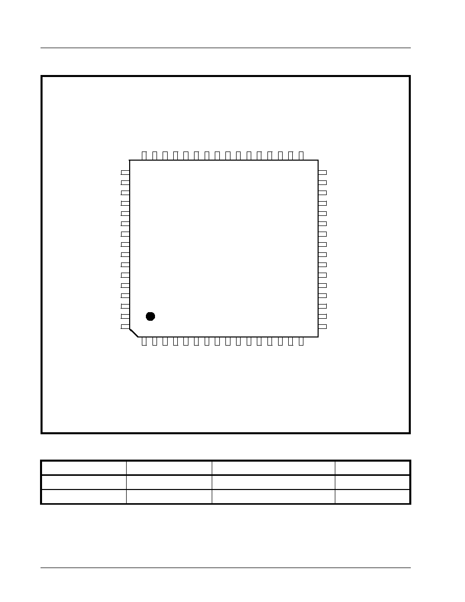
F
IGURE
2. P
IN
O
UT
A
SSIGNMENT
ORDERING INFORMATION
P
ART
N
UMBER
P
ACKAGE
O
PERATING
T
EMPERATURE
R
ANGE
D
EVICE
S
TATUS
XR16L784CV
64-Lead TQFP
0°C to +70°C
Active
XR16L784IV
64-Lead TQFP
-40°C to +85°C
Active
X R 1 6 L 7 8 4
6 4 -T Q F P
TX
1
DTR1#
RTS
1
#
RI
1
#
CD1#
DSR1#
CTS
1
#
RX1
TX
2
DTR2#
RTS
2
#
RI
2
#
CD2#
DSR2#
CTS
2
#
RX2
R X 0
C T S 0 #
D S R 0 #
C D 0 #
R I0 #
R T S 0 #
D T R 0 #
T X 0
V C C
G N D
X T A L 1
X T A L 2
2
4
5
6
7
9
8
3
1
1 0 1 1
1 3
1 2
1 4 1 5 1 6
3 4 3 3
3 5
3 6
3 7
3 8
3 9
4 0
4 1
4 2
4 3
4 4
4 5
4 6
4 7
4 8
50
49
64
63
62
61
60
59
58
57
55
56
54
53
52
51
31
32
17
18
19
20
21
22
23
24
26
25
27
28
29
30
E N IR
T M R C K
V C C
G N D
C D 3 #
D S R 3 #
C T S 3 #
R X 3
T X 3
D T R 3 #
R T S 3 #
R I3 #
R S T #
1 6 /6 8 #
D 7
D 6
IN T #
C S #
A 0
A 1
A2
A3
A4
A5
A6
A7
IO
R#
IO
W
#
VCC
GND
D0
D1
D2
D3
D4
D5
áç
áç
áç
áç
XR16L784
REV. 1.2.0
HIGH PERFORMANCE 2.97V TO 5.5V QUAD UART
3
PIN DESCRIPTIONS
Pin Descriptions
N
AME
P
IN
#
T
YPE
D
ESCRIPTION
DATA BUS INTERFACE
A7-A0
6-1,64,63
I
Address data lines [7:0]. A0:A3 selects individual UART's 16 configuration
registers, A4:A6 selects UART channel 0 to 3, and A7 selects the global
device configuration registers
D7:D0
18-11
IO
Data bus lines (7:0] (bidirectional).
IOR#
7
I
When 16/68# pin is HIGH, it selects Intel bus interface and this input is read
strobe (active low). The falling edge instigates an internal read cycle and
retrieves the data byte from an internal register pointed by the address lines
[A7:A0], puts it on the data bus to allow the host processor to read it on the
leading edge.
When 16/68# pin is LOW, it selects Motorola bus interface and this input
should be connected to VCC.
IOW#
(R/W#)
8
I
When 16/68# pin is HIGH, it selects Intel bus interface and this input
becomes write strobe (active low). The falling edge instigates the internal
write cycle and the leading edge transfers the data byte on the data bus to an
internal register pointed by the address lines.
When 16/68# pin is LOW, it selects Motorola bus interface and this input
becomes read (logic 1) and write (logic 0) signal.
CS#
62
I
When 16/68# pin is HIGH, this input is chip select (active low) to enable the
XR16L784 device.
When 16/68# pin is LOW, this input becomes the read and write strobe
(active low) for the Motorola bus interface.
INT#
61
OD
Global interrupt output from XR16L784 (open drain, active low). This output
requires an external pull-up resistor (47K-100K ohms) to operate properly. It
may be shared with other devices in the system to form a single interrupt line
to the host processor and have the software driver polls each device for the
interrupt status.
MODEM OR SERIAL I/O INTERFACE
TX0
53
O
UART channel 0 Transmit Data or infrared transmit data. Normal TXD output
idles HIGH while infrared TXD output idles LOW.
RX0
60
I
UART channel 0 Receive Data or infrared receive data. Normal RXD input
idles HIGH while infrared RXD input idles LOW. In the infrared mode, the
polarity of the incoming RXD signal can be selected via FCTR bit-4. If this bit
is a logic 0, a LOW on the RXD input is considered a mark and if this bit is a
logic 1, a HIGH on the RXD input is considered a space.
RTS0#
55
O
UART channel 0 Request to Send or general purpose output (active low).
This port must be asserted prior using for one of two functions:
1) auto RTS flow control, see EFR bit-6, MCR bits-1 & 2, FCTR bits 0-3 and
IER bit-6
2) Auto RS485 half-duplex direction control, see FCTR bit-5, MCR bit-2 and
MSR bits 4-7.
CTS0#
59
I
UART channel 0 Clear to Send or general purpose input (active low). It can be
used for auto CTS flow control, see EFR bit-7, MCR bit-2 and IER bit-7.
XR16L784
áç
áç
áç
áç
HIGH PERFORMANCE 2.97V TO 5.5V QUAD UART
REV. 1.2.0
4
DTR0#
54
O
UART channel 0 Data Terminal Ready or general purpose output (active low).
This port must be asserted prior using for one of two functions:
1) auto DTR flow control, see EFR bit-6, FCTR bits-0 to 3, MCR bits-0 & 2,
and IER bit-6
2) Auto RS485 half-duplex direction control, see FCTR bit-5, MCR bit-2 and
MSR bit 4-7.
DSR0#
58
I
UART channel 0 Data Set Ready or general purpose input (active low). It can
be used for auto DSR flow control, see EFR bit-7, MCR bit-2 and IER bit-7.
CD0#
57
I
UART channel 0 Carrier Detect or general purpose input (active low).
RI0#
56
I
UART channel 0 Ring Indicator or general purpose input (active low).
TX1
48
O
UART channel 1 Transmit Data or infrared transmit data. Normal TXD output
idles HIGH while infrared TXD output idles LOW.
RX1
41
I
UART channel 1 Receive Data or infrared receive data. Normal RXD input
idles HIGH while infrared RXD input idles LOW. In the infrared mode, the
polarity of the incoming RXD signal can be selected via FCTR bit-4. If this bit
is a logic 0, a LOW on the RXD input is considered a mark and if this bit is a
logic 1, a HIGH on the RXD input is considered a space.
RTS1#
46
O
UART channel 1 Request to Send or general purpose output (active low).
See description of RTS0# pin.
CTS1#
42
I
UART channel 1 Clear to Send or general purpose input (active low). See
description of CTS0# pin.
DTR1#
47
O
UART channel 1 Data Terminal Ready or general purpose output (active low).
See description of DTS0# pin.
DSR1#
43
I
UART channel 1 Data Set Ready or general purpose input (active low). See
description of DSR0# pin.
CD1#
44
I
UART channel 1 Carrier Detect or general purpose input (active low).
RI1#
45
I
UART channel 1 Ring Indicator or general purpose input (active low).
TX2
40
O
UART channel 2 Transmit Data or infrared transmit data. Normal TXD output
idles HIGH while infrared TXD output idles LOW.
RX2
33
I
UART channel 2 Receive Data or infrared receive data. Normal RXD input
idles HIGH while infrared RXD input idles LOW. In the infrared mode, the
polarity of the incoming RXD signal can be selected via FCTR bit-4. If this bit
is a logic 0, a LOW on the RXD input is considered a mark and if this bit is a
logic 1, a HIGH on the RXD input is considered a space.
RTS2#
38
O
UART channel 2 Request to Send or general purpose output (active low).
See description of RTS0# pin.
CTS2#
34
I
UART channel 2 Clear to Send or general purpose input (active low). See
description of CTS0# pin.
DTR2#
39
O
UART channel 2 Data Terminal Ready or general purpose output (active low).
See description of DTS0# pin.
DSR2#
35
I
UART channel 2 Data Set Ready or general purpose input (active low). See
description of DSR0# pin.
CD2#
36
I
UART channel 2 Carrier Detect or general purpose input (active low).
RI2#
37
I
UART channel 2 Ring Indicator or general purpose intput (active low).
Pin Descriptions
N
AME
P
IN
#
T
YPE
D
ESCRIPTION
áç
áç
áç
áç
XR16L784
REV. 1.2.0
HIGH PERFORMANCE 2.97V TO 5.5V QUAD UART
5
N
OTE
: Pin type: I=Input, O=Output, IO= Input/output, OD=Output Open Drain.
TX3
28
O
UART channel 3 Transmit Data or infrared transmit data. Normal TXD output
idles HIGH while infrared TXD output idles LOW.
RX3
21
I
UART channel 3 Receive Data or infrared receive data. Normal RXD input
idles HIGH while infrared RXD input idles LOW. In the infrared mode, the
polarity of the incoming RXD signal can be selected via FCTR bit-4. If this bit
is a logic 0, a LOW on the RXD input is considered a mark and if this bit is a
logic 1, a HIGH on the RXD input is considered a space.
RTS3#
26
O
UART channel 3 Request to Send or general purpose output (active low).
See description of RTS0# pin.
CTS3#
22
I
UART channel 3 Clear to Send or general purpose input (active low).d. See
description of CTS0# pin.
DTR3#
27
O
UART channel 3 Data Terminal Ready or general purpose output (active low).
See description of DTS0# pin.
DSR3#
23
I
UART channel 3 Data Set Ready or general purpose input (active low). See
description of DSR0# pin.
CD3#
24
I
UART channel 3 Carrier Detect or general purpose input (active low).
RI3#
25
I
UART channel 3 Ring Indicator or general purpose input (active low).
ANCILLARY SIGNALS
XTAL1
50
I
Crystal or external clock input. Caution: this input is not 5V tolerant.
XTAL2
49
O
Crystal or buffered clock output.
TMRCK
31
I
16-bit timer/counter external clock input.
ENIR
32
I
Infrared mode enable (active high). This pin is sampled during power up, fol-
lowing a hardware reset (RST#) or soft-reset (register RESET). It can be
used to start up all 8 UARTs in the infrared mode. The sampled logic state is
transferred to MCR bit-6 in the UART.
RST#
20
I
Reset (active low). The configuration and UART registers are reset to default
values, see Table-15.
16/68#
19
I
Intel or Motorola data bus interface select. HIGH selects Intel bus interface
and LOW selects Motorola interface. This input affects the functionality of
IOR#, IOW# and CS# pins.
VCC
9,30,52
+5V or +3.3V supply, all inputs are 5V tolerant except for XTAL1.
GND
10,29,51
Power supply common, ground.
Pin Descriptions
N
AME
P
IN
#
T
YPE
D
ESCRIPTION
Document Outline