 | –≠–ª–µ–∫—Ç—Ä–æ–Ω–Ω—ã–π –∫–æ–º–ø–æ–Ω–µ–Ω—Ç: XR-2209 | –°–∫–∞—á–∞—Ç—å:  PDF PDF  ZIP ZIP |
XR-2209
...the analog plus company
TM
Voltage-Controlled
Oscillator
Rev. 2.02
E
1975
EXAR Corporation, 48720 Kato Road, Fremont, CA 94538
z
(510) 688-7000
z
FAX (510) 688-7017
1
June 1997≠3
FEATURES
D
Excellent Temperature Stability (20ppm/
∞
C)
D
Linear Frequency Sweep
D
Wide Sweep Range (1000:1 Minimum)
D
Wide Supply Voltage Range (+4V to +13V)
D
Low Supply Sensitivity (0.1% /V)
D
Wide Frequency Range (0.01Hz to 1MHz)
D
Simultaneous Triangle and Squarewave Outputs
APPLICATIONS
D
Voltage and Current-to-Frequency Conversion
D
Stable Phase-Locked Loop
D
Waveform Generation
Triangle, Sawtooth, Pulse, Squarewave
D
FM and Sweep Generation
GENERAL DESCRIPTION
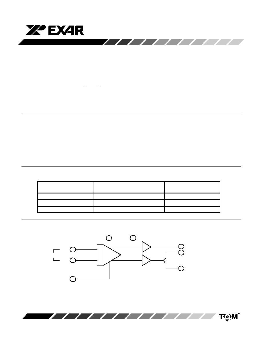
The XR-2209 is a monolithic voltage-controlled oscillator
(VCO) integrated circuit featuring excellent frequency
stability and a wide tuning range. The circuit provides
simultaneous triangle and squarewave outputs over a
frequency range of 0.01Hz to 1MHz. It is ideally suited for
FM, FSK, and sweep or tone generation, as well as for
phase-locked loop applications.
The oscillator of the XR-2209 has a typical drift
specification of 20ppm/
∞
C. The oscillator frequency can
be linearly swept over a 1000:1 range with an external
control voltage.
ORDERING INFORMATION
Part No.
Package
Operating
Temperature Range
XR-2209CN
8 Lead 300 Mil CDIP
0
∞
to +70
∞
C
XR-2209M
8 Lead 300 Mil CDIP
-55
∞
C to +125
∞
C
XR-2209CP
8 Lead 300 Mil PDIP
0
∞
C to +70
∞
C
BLOCK DIAGRAM
Square Wave Out
Triangle Wave Out
TWO
SWO
A1
A2
BIAS
5
7
8
VCO
2
3
1
V
CC
Timing
Capacitor
C1
C2
4
Timing
R
Resistor
6
V
EE
Figure 1. XR-2209 Block Diagram
XR-2209
2
Rev. 2.02
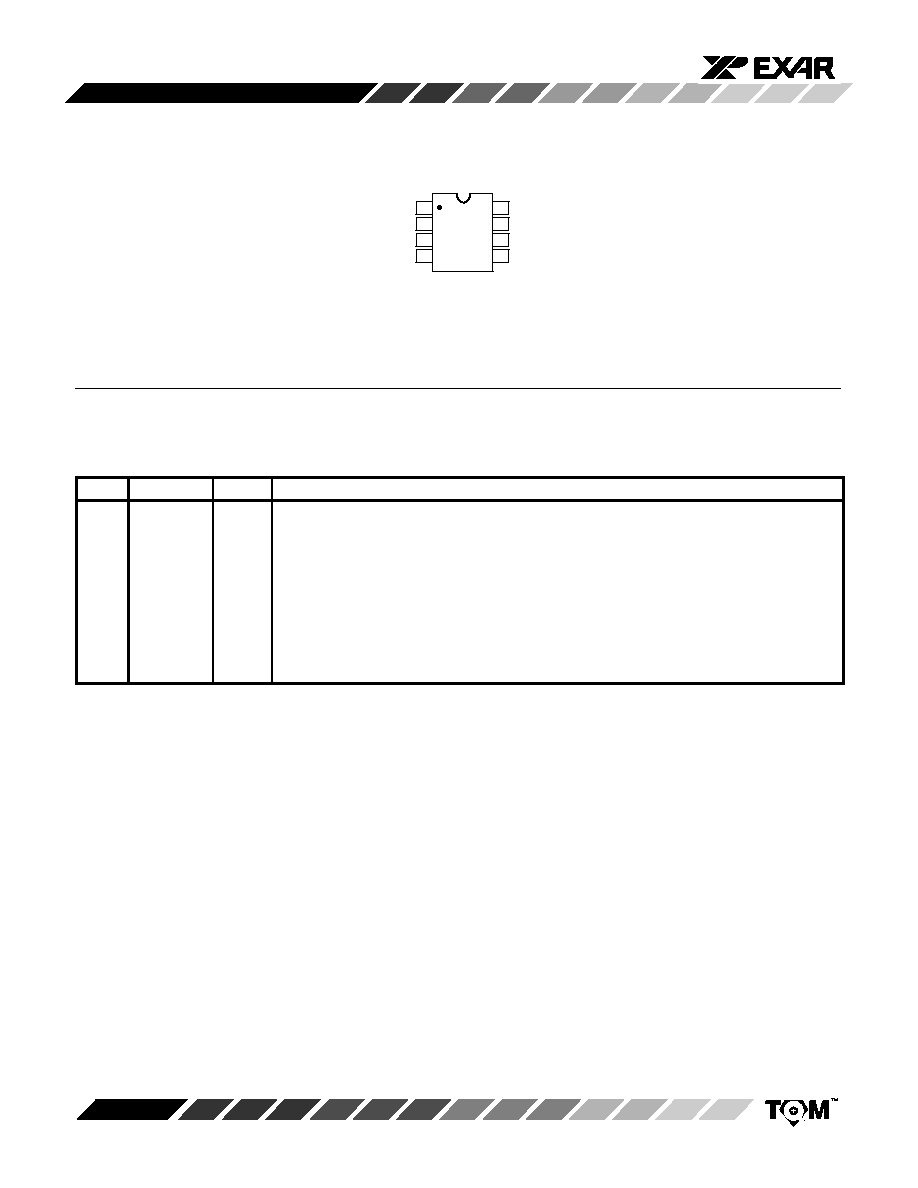
PIN CONFIGURATION
TWO
SWO
V
EE
BIAS
8 Lead PDIP, CDIP (0.300")
1
2
3
4
8
7
6
5
V
CC
C1
C2
TR
PIN DESCRIPTION
Pin #
Symbol
Type
Description
1
V
CC
Positive Power Supply.
2
C1
I
Timing Capacitor Input.
3
C2
I
Timing Capacitor Input.
4
TR
I
Timing Resistor.
5
BIAS
I
Bias Input for Single Supply Operation.
6
V
EE
Negative Power Supply.
7
SWO
O
Square Wave Output Signal.
8
TWO
O
Triangle Wave Output Signal.
XR-2209
Rev. 2.02
3
DC ELECTRICAL CHARACTERISTICS
Test Conditions: Test Circuit of
Figure 3 and Figure 4, V
CC
= 12V, T
A
= +25
∞
C, C = 5000pF, R = 20k
W
, R
L
=
4.7k
W
, S
1
and S
2
Closed Unless Otherwise Specified
XR-2209M
XR-2209C
Parameters
Min.
Typ.
Max.
Min.
Typ.
Max.
Units
Conditions
General Characteristics
Supply Voltage
Single Supply
Split Supplies
8
"
4
26
"
13
8
"
4
26
"
13
V
V
See
Figure 3
Figure 4
Supply Current
Single Supply
5
7
5
8
mA
Figure 3
Measured at Pin 1, S
1
, S
2
Open
Split Supplies
Positive
Negative
5
4
7
6
5
4
8
7
mA
mA
Figure 4
Measured at Pin 1, S
1
, S
2
Open
Measured at Pin 4, S
1
, S
2
Open
Oscillator Section - Frequency Characteristics
Upper Frequency Limit
0.5
1.0
0.5
1.0
MHz
C = 500pF, R = 2K
W
Lowest Practical Frequency
0.01
0.01
Hz
C = 50
m
F, R = 2M
W
Frequency Accuracy
"
1
"
3
"
1
"
5
% of f
o
Frequency Stability
Temperature
Power Supply
20
0.15
50
30
0.15
ppm/
∞
C
%/V
0
∞
C < T
A
< 70
∞
C
Sweep Range
1000:
1
3000:1
1000:
1
f
H
/f
L
R = 1.5 K
W
for f
H
R = 2M
W
for f
L
Sweep Linearity
10:1 Sweep
1000:1 Sweep
1
5
2
1.5
5
%
%
f
H
= 10kHz, f
L
= 1kHz
f
H
= 100kHz, f
L
= 100Hz
FM Distortion
0.1
0.1
%
+10% FM Deviation
Recommended Range of
Timing Resistor
1.5
2000
1.5
2000
k
W
See Characteristic Curves
Impedance at Timing Pins
75
75
W
Measured at Pin 4
Output Characteristics
Triangle Output
Amplitude
Impedance
DC Level
Linearity
4
6
10
+100
0.1
4
6
10
+100
0.1
Vpp
W
mV
%
Measured at Pin 8
Referenced to Pin 6
From 10% to 90% of Swing
Squarewave Output
Amplitude
Saturation Voltage
Rise Time
Fall Time
11
12
0.2
200
20
0.4
11
12
0.2
200
20
0.4
Vpp
V
nsec
nsec
Measured at Pin 7, S
2
Closed
Referenced to Pin 6
C
L
10pF, R
L
= 4.7K
C
L
10pF
Notes
Bold face parameters are covered by production test and guaranteed over operating temperature range.
Specifications are subject to change without notice
XR-2209
4
Rev. 2.02
ABSOLUTE MAXIMUM RATINGS
Power Supply
26V
. . . . . . . . . . . . . . . . . . . . . . . . . . . . . . .
Power Dissipation (package limitation)
Ceramic package
750mW
. . . . . . . . . . . . . . . . . . . . . . .
Derate above +25
∞
C
10mW/
∞
C
. . . . . . . . . . . . . . . . . .
Plastic package
600mW
. . . . . . . . . . . . . . . . . . . . . . . . .
Derate above +25
∞
C
8mW/
∞
C
. . . . . . . . . . . . . . . . . . .
SOIC package
300mW
. . . . . . . . . . . . . . . . . . . . . . . . . .
Derate above +25
∞
C
4mW/
∞
C
. . . . . . . . . . . . . . . . . . .
Storage Temperature Range
-
65
∞
C to +150
∞
C
. . . . . . .
2R
1
V
CC
Q13
Q14
Q15
R
Q1
Q2
Q3
Q4
Q5
R2
Q6
Q7
R
R1
Q8
2
Q12
3
Q9
Q19
Timing
Capacitor
R
Q10
Q11
R3
R4
R
2R
Triangle Wave
8
Output
Q27
Square Wave
7
Output
4R
Q20
R6
R5
R7
Q21
4
BIAS
5
Q22
Q24
Q23
Q25
Q26
Figure 2. Equivalent Schematic Diagram
¡
6
V
EE
Timing Resistor
XR-2209
Rev. 2.02
5
PRECAUTIONS
The following precautions should be observed when
operating the XR-2209 family of integrated circuits:
1.
Pulling excessive current from the timing terminals
will adversely affect the temperature stability of the
circuit. To minimize this disturbance, it is
recommended that the total current drawn from pin 4
be limited to
6mA. In addition, permanent damage
to the device may occur if the total timing current
exceeds 10mA.
2.
Terminals 2, 3, and 4 have very low internal
impedance and should, therefore, be protected from
accidental shorting to ground or the supply voltage.
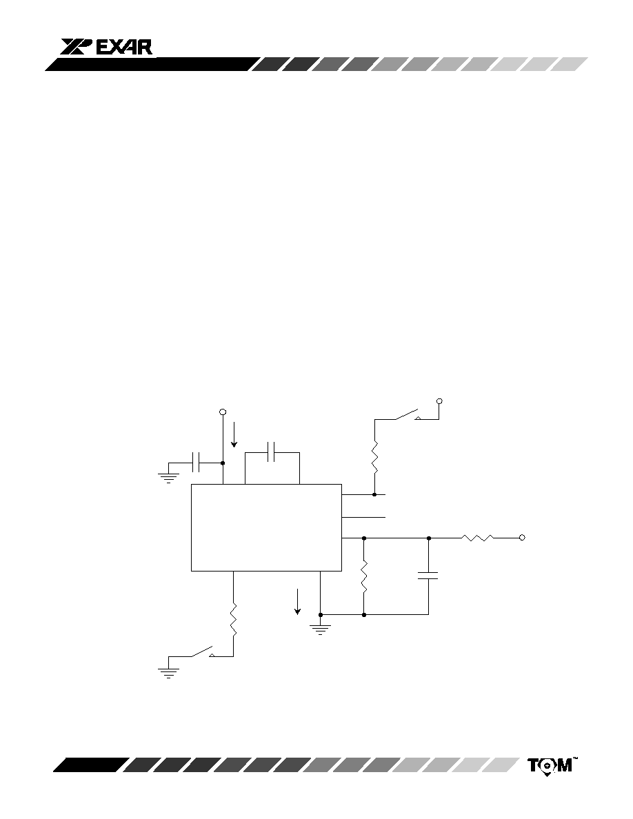
SYSTEM DESCRIPTION
The XR-2209 functional blocks are shown in the block
diagram given in
Figure 1. They are a voltage controlled
oscillator (VCO), and two buffer amplifiers for triangle and
squarewave outputs.
Figure 2 is a simplified XR-2209
schematic diagram that shows the circuit in greater detail.
The VCO is a modified emitter-coupled current controlled
multivibrator. Its oscillation is inversely proportional to the
value of the timing capacitor connected to pins 2 and 3,
and directly proportional to the total timing current I
T
. This
current is determined by the resistor that is connected
from the timing terminals (pin 4) to ground.
The triangle output buffer has a low impedance output
(10
W
typ.) while the squarewave is an open-collector
type. An external bias input allows the XR-2209 to be
used in either single or split supply applications.
R
L
Square Wave
Output
V
CC
Triangle Wave
S2
C
V
CC
1
m
F
I +
TR
4
V
EE
6
BIAS
5
TWO
8
SWO
7
C 2
3
C1
2
1
XR-2209
S1
R
Output
1
m
F
I-
5.1K
5.1K
Figure 3. Test Circuit for Single Supply Operation
V
CC
V
CC