EXAR Corporation, 48720 Kato Road, Fremont, CA 94538
∑
(510) 668-7000
∑
FAX (510) 668-7017
XR68C92/192
Rev. P1.00
PLCC Package
Preliminary Information
DUAL UNIVERSAL ASYNCHRONOUS
RECEIVER AND TRANSMITTER
DESCRIPTION
The XR68C92/192 is a Dual Universal Asynchronous Receiver and Transmitter with 8 (XR68C92) / 16
(XR68C192) bytes transmit and receive FIFO. The XR68C92/192 is a pin and functional compatible for the
XR68C681 and Philips SCC68681 UART with additional features. The operating speed of the receiver and
transmitter can be selected independently from a table of twenty four fixed baud rates, a 16X clock derived from
a programmable counter/timer, or an external 1X or 16X clock. The baud rate generator and counter/timer can
operate directly from a crystal or from external clock input. The XR68C92/192 provides a power down mode in
which the oscillator is stopped but the register contents are retained. The XR68C92/192 is fabricated in an
advanced CMOS process to achieve low power and high speed requirements.
FEATURES
∑
Pin to pin and functional compatible to XR68C681
and SCC68692
∑
Full duplex asynchronous transmit receive opera-
tion
∑
8 Bytes transmit/receive FIFO (XR68C92)
∑
16 Bytes transmit/receive FIFO (XR68C192)
∑
Programmable character lengths (5, 6, 7, 8)
∑
Parity, framing, and over run error detection
∑
Programmable 16-bit timer/counter
∑
On-chip crystal oscillator
∑
Single interrupt output with eight selectable inter-
rupting conditions
∑
External 1X or 16X clock
∑
Data rate up to 1Mbps
∑
Fixed baud rates from 50bps to 230.4kbps
∑
6 General purpose inputs
∑
8 General purpose outputs
∑
TTL compatible inputs, outputs
∑
4 Transmit/receive trigger levels
∑
Watch dog timer
∑
Multidrop mode operation
∑
3.3 or 5 volts operation
∑
Loopback modes
∑
Power down mode
ORDERING INFORMATION
Part number
Pins Package
Operating temperature
XR68C92CP
40
PDIP
0∞ C to + 70∞ C
XR68C92CJ
44
PLCC
0∞ C to + 70∞ C
XR68C92CV
44
TQFP
0∞ C to + 70∞ C
Part number
Pins Package
Operating temperature
XR68C92IP
40
PDIP
-40∞ C to + 85∞ C
XR68C92IJ
44
PLCC
-40∞ C to + 85∞ C
XR68C92IV
44
TQFP
-40∞ C to + 85∞ C
XR68C192CP
40
PDIP
0∞ C to + 70∞ C
XR68C192CJ
44
PLCC
0∞ C to + 70∞ C
XR68C192CV
44
TQFP
0∞ C to + 70∞ C
XR68C192IP
40
PDIP
-40∞ C to + 85∞ C
XR68C192IJ
44
PLCC
-40∞ C to + 85∞ C
XR68C192IV
44
TQFP
-40∞ C to + 85∞ C
6
5
4
3
2
1
44
43
42
41
40
7
8
9
10
11
12
13
14
15
16
17
39
38
37
36
35
34
33
32
31
30
29
18
19
20
21
22
23
24
25
26
27
28
A4
IP0
R/-W
-DTACK
RXB
N.C.
TXB
OP1
OP3
OP5
OP7
-CS
-RESET
XTAL2
XTAL1
RXA
N.C.
TXA
OP0
OP2
OP4
OP6
D1
D3
D5
D7
GN
D
N.C
.
-I
NT
D6
D4
D2
D0
A3
IP
1
A2
IP
3
A1
N.C
.
VC
C
IP
4
IP
5
-i
a
c
k
IP
2
XR68C92
XR68C192
XR68C92/192
2
Rev. P1.00
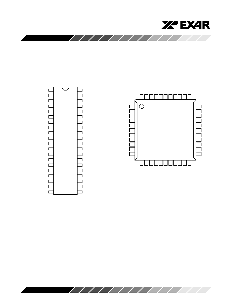
40 Pin DIP Package
44 Pin TQFP Package
Package Description
1
2
3
4
5
6
7
8
9
10
11
12
13
14
15
16
17
18
19
20
40
39
38
37
36
35
34
33
32
31
30
29
28
27
26
25
24
23
22
21
A1
IP3
A2
IP1
A3
A4
IP0
R/-W
-DTACK
RXB
TXB
OP1
OP3
OP5
OP7
D1
D3
D5
D7
GND
VCC
IP4
IP5
-IACK
IP2
-CS
-RESET
XTAL2
XTAL1
RXA
TXA
OP0
OP2
OP4
OP6
D0
D2
D4
D6
-INT
XR
6
8
C
9
2
X
R
68
C
1
92
44
43
42
41
40
39
38
37
36
35
34
1
2
3
4
5
6
7
8
9
10
11
33
32
31
30
29
28
27
26
25
24
23
12
13
14
15
16
17
18
19
20
21
22
A3
IP0
-IOW
-DTACK
RXB
TXB
OP1
OP3
OP5
OP7
N.C.
-CS
RESET
XTAL2
XTAL1
RXA
TXA
OP0
OP2
OP4
OP6
N.C.
A2
IP
1
A1
IP
3
A0
VC
C
VC
C
IP
4
IP
5
-I
A
C
K
IP
2
D1
D3
D5
D7
GN
D
GN
D
-I
NT
D6
D4
D2
D0
XR88C92
XR88C192
XR68C92/192
3
Rev. P1.00
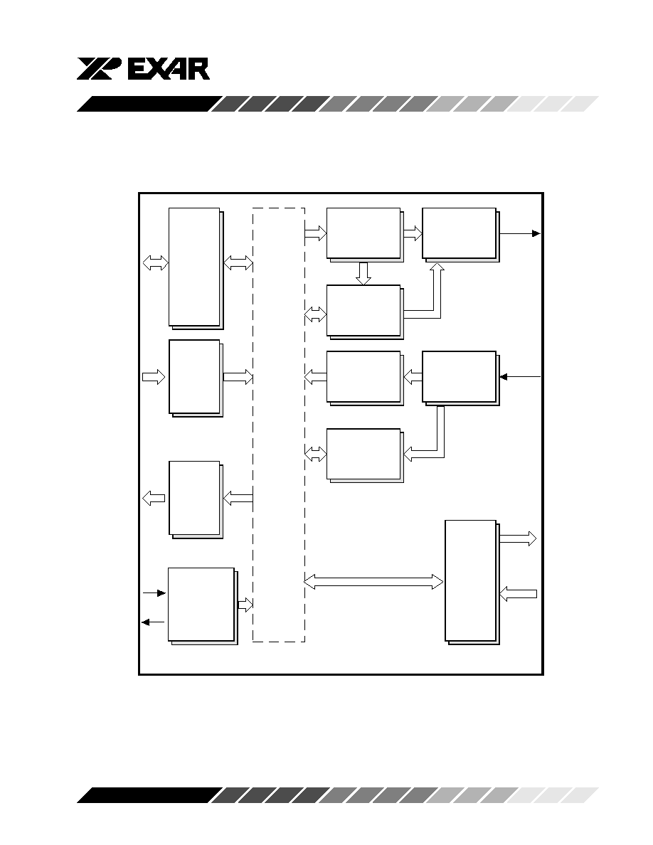
Block Diagram
D0-D7
R/-W
-RESET
-DTACK
-IACK
A1-A4
-CS
-INT
-RXARDY
-RXBRDY
-TXARDY
-TXBRDY
OP0-OP7
IP0-IP5
TX A/B
RX A/B
XTAL1
XTAL2
Data
bu
s
&
C
o
n
t
rol Lo
gic
Reg
i
st
er
S
e
l
ect
L
ogic
I/O
Control
Logic
In
t
e
rr
u
p
t
Co
n
t
r
o
l
L
ogic
Transmit
FIFO
Registers
Flow
Control
Logic
Transmit
Shift
Register
Receive
FIFO
Registers
Flow
Control
Logic
Receive
Shift
Register
In
t
e
r Co
n
n
e
c
t Bu
s
Li
ne
s
&
C
o
n
t
rol s
i
gnals
C
l
oc
k
&
Ba
u
d
Ra
te
Gen
e
r
a
t
o
r
XR68C92/192
4
Rev. P1.00
SYMBOL DESCRIPTION (* 44 TQFP Package)
Symbol
Pin
Signal
Pin Description
44
40
44*
type
-DTACK
10
9
4
O
Data transfer acknowledge (three-state active low output).
During Read, Write, or interrupt cycle goes low to indicate
proper transfer of data between the CPU and XR68C92/
192.
RX A/B
35,11
31,10
29,5
I
Serial data input. The serial information (data) received
from serial port to XR68C92/192 receive input circuit. A
mark (high) is logic one and a space (low) is logic zero.
TX A/B
33,13
30,11
28,6
O
Serial data output. The serial data is transmitted via this pin
with additional start , stop and parity bits. The TX will be held
in mark (high) state during reset, local loop back mode or
when the transmitter is disabled.
OP0
32
29
27
O
Multi-purpose output. General purpose output or Channel A
Request-To-Send (-RTSA active low).
OP1
14
12
7
O
Multi-purpose output. General purpose output or Channel B
Request-To-Send (-RTSB active low).
OP2
31
28
26
O
Multi-purpose output. General purpose output or one of the
following functions can be selected for this output pin by
programming the auxiliary control register Bit 1,0;
TxAClk1 -Transmit 1X clock.
TxAClk16 -Transmit 16X clock
RxAClk1 -Receive 1X clock
OP3
15
13
8
O
Multi-purpose output. General purpose output or one of the
following functions can be selected for this output pin by
programming the auxiliary control register Bit 3,2;
C/T -Counter timer output (Open drain output)
TxBClk1 -Transmit 1X clock
RxBClk1 -Receive 1X clock
OP4
30
27
25
O
Multi-purpose output. General purpose output or one of the
following functions can be selected for this output pin by
programming the auxiliary control register;
-RxARDY -Receive ready signal (Open drain output)
-RxAFULL - Receive FIFO full signal (Open drain output)
XR68C92/192
5
Rev. P1.00
SYMBOL DESCRIPTION (* 44 TQFP Package)
Symbol
Pin
Signal
Pin Description
44
40
44*
type
OP5
16
14
9
O
Multi-purpose output. General purpose output or one of the
following functions can be selected for this output pin by
programming the auxiliary control register;
-RxBRDY - Receive ready signal (Open drain output)
-RxBFULL - Receive FIFO full signal (Open drain output)
OP6
29
26
24
O
Multi-purpose output. General purpose output or Transmit
A holding register empty interrupt (-TxARDY Open drain
output).
OP7
17
15
10
O
Multi-purpose output. General purpose output or Transmit
B holding register empty interrupt (-TxBRDY Open drain
output)
A1-A4
2,4,
1,3,
40,42,
6,7
5,6
44,1
I
Address select lines. To select internal registers.
XTAL1
36
32
30
I
Crystal input 1 or external clock input. A crystal can be
connected to this pin and XTAL2 pin to utilize the internal
oscillator circuit. An external clock can be used to clock
internal circuit and baud rate generator for custom transmis-
sion rates.
XTAL2
37
33
31
O
Crystal input 2 or buffered clock output. See XTAL1.
-RESET
38
34
32
I
Master reset. (active low) A low on this pin will reset all the
outputs and internal registers. The transmitter output and
the receiver input will be disabled during reset time.
GND
22
20
16,17
Pwr
Signal and power ground.
-INT
24
21
18
O
Interrupt output (open drain active low) This pin goes low
(when enabled by the selectable interrupt mask register)
upon occurrence of one or more of eight mask-able interrupt
conditions. CPU can read the interrupt status register to
determine the interrupting condition(s). This output requires
a pull-up resistor.
IP0
8
7
2
I
Multi-purpose input or Channel A Clear-To-Send (-CTSA
active low).