 | –≠–ª–µ–∫—Ç—Ä–æ–Ω–Ω—ã–π –∫–æ–º–ø–æ–Ω–µ–Ω—Ç: XRD6414A | –°–∫–∞—á–∞—Ç—å:  PDF PDF  ZIP ZIP |
XRD6414
...the analog plus company
TM
CMOS 10-Bit, 20 MSPS, High Speed
Analog-to-Digital Converter
with 4:1 Input Analog Multiplexer
Rev. 1.00
E
1996
EXAR Corporation, 48720 Kato Road, Fremont, CA 94538
z
(510) 668-7000
z
FAX (510) 668-7017
March 1997≠3
FEATURES
D
10-Bit Resolution
D
20MHz Sampling Rate
D
4:1 Analog Input Multiplexer
D
Internal S/H Function
D
Single 5.0V Power Supply
D
V
IN
DC Range: 0V to V
DD
D
V
REF
DC Range: 1V to V
DD
D
Low Power: 120mW (typ)
D
Three-State Digital Outputs
D
Power Down: 1.5mW (typ) Power Dissipation
D
ESD Protection: 2000V Minimum
D
For 3V Operation Refer to XRD64L14
APPLICATIONS
D
Multiplexed Data Acquisition
D
Precision Scanners
D
Digital Color Copiers
D
Test and Scientific Instruments
D
Digital Cameras
D
Medical Imaging
D
IR Imaging
BENEFITS
D
Complete Analog-to-Digital Converter (ADC) that
Requires no External Active Components
D
Small Outline Package to Reduce Board Space
D
Low Power Dissipation
D
Easy to Use Rugged Design
GENERAL DESCRIPTION
The XRD6414 is a 10-bit, 20 MSPS, Analog-to-Digital
Converter (ADC) with a 4:1 Analog Input Multiplexer for
applications that require high speed and high accuracy.
Designed using an advanced CMOS process, this part
offers excellent performance, low power consumption
and latch-up free operation.
The XRD6414 uses a subranging architecture to maintain
low power consumption at high conversion rates. Our
proprietary comparator design achieves a low analog
input capacitance. The input circuitry of the XRD6414
includes an on-chip S/H function that allows the product to
digitize analog input signals between AGND and AV
DD
.
The XRD6414 can be placed into power down (stand-by)
mode, reducing the power dissipation to 1.5mW (typical)
by a digitally controlled pin.
Providing external reference voltages allows easy
interface to any input signal range between AGND and
AV
DD
. This also allows the system to calibrate out zero
scale and full scale errors by adjusting V
RT
and V
RB
. A
separate power supply pin, DV
DD,
sets the output logic
levels for 3V or 5V interface.
This device operates from a single 5.0V supply. Power
consumption from a 5.0V supply is typically 120mW at
F
S
=15MHz. For 3.3V power supply operation refer to
XRD64L14.
ORDERING INFORMATION
Part No.
Package
Operating
Temperature Range
XRD6414AIQ
32 Lead TQFP (7 x 7 x 1.4 mm)
≠40
∞
C to +85
∞
C
XRD6414
2
Rev. 1.00
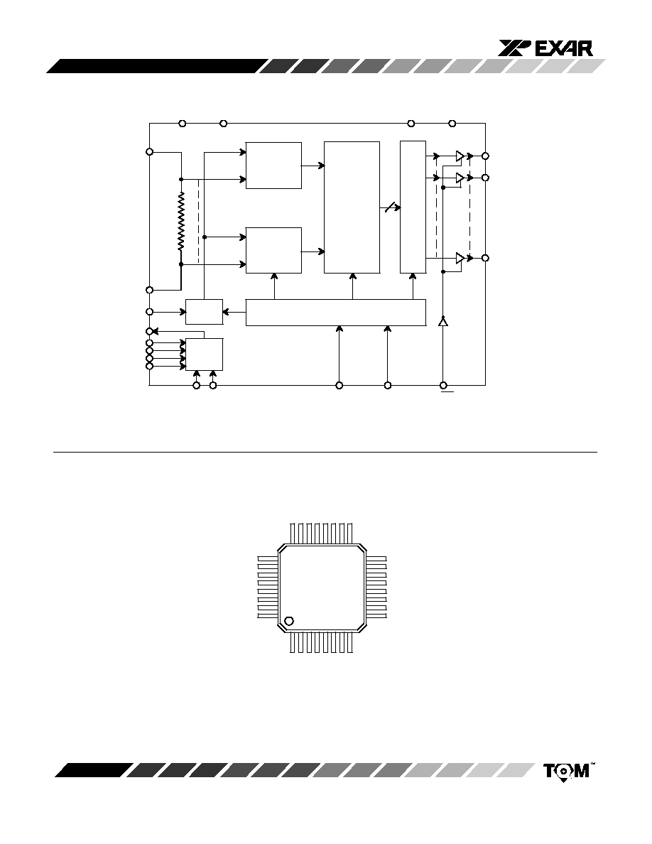
F/F
Clock and Control Logic
THA
Encoder
and
Error
Correction
V
RT
AV
DD
(3)
A1
AGND(3)
CLK
DB9 (MSB)
DB0 (LSB)
OE
Latched
MSB
Comparators
PD
11
A0
4:1
MUX
A
IN
1
A
OUT
V
IN
OFW
Latched
LSB
Comparators
V
RB
A
IN
2
A
IN
3
A
IN
4
R
L
DV
DD
DGND
Figure 1. Simplified Block Diagram
PIN CONFIGURATION
32 Lead TQFP (7 x 7 x 1.4 mm)
24
17
16
9
1
8
25
32
XRD6414
3
Rev. 1.00
PIN DESCRIPTION
Pin #
Symbol
Description
1
DB9
Data Output Bit 9 (MSB)
2
DGND
Ground (Digital Outputs)
3
AGND
Ground
4
A0
MUX Select Bit 0
5
A1
MUX Select Bit 1
6
AV
DD
Power Supply
7
CLK
Sampling Clock Input
8
OE
Output Enable Control
9
PD
Power Down Control
10
AV
DD
Power Supply
11
AGND
Ground
12
V
RT
Top of Reference Ladder
13
V
RB
Bottom of Reference Ladder
14
A
IN
4
MUX Analog Signal Input 4
15
A
IN
3
MUX Analog Signal Input 3
16
AGND
Ground
17
A
IN
2
MUX Analog Signal Input 2
18
A
IN
1
MUX Analog Signal Input 1
19
A
OUT
MUX Analog Signal Output
20
V
IN
Analog Input Voltage to ADC
21
AV
DD
Power Supply
22
DV
DD
Power Supply (Digital Outputs)
23
OFW
Overflow Output
24
DB0
Data Output Bit 0 (LSB)
25
DB1
Data Output Bit 1
26
DB2
Data Output Bit 2
27
DB3
Data Output Bit 3
28
DB4
Data Output Bit 4
29
DB5
Data Output Bit 5
30
DB6
Data Output Bit 6
31
DB7
Data Output Bit 7
32
DB8
Data Output Bit 8
XRD6414
4
Rev. 1.00
ELECTRICAL CHARACTERISTICS
Unless Otherwise Specified: AV
DD
= DV
DD
= 5.0V, F
S
= 15MHz (50% Duty Cycle),
V
RT
= 5.0V, V
RB
= 0.0V, T
A
= 25
∞
C
Symbol
Parameter
Min.
Typ.
Max.
Unit
Conditions
Key Features
n
Resolution
10
Bits
F
S
Maximum Sample Rate
20
15
MSPS
DC Accuracy
1
DNL
Differential Non-Linearity
≠0.8
0.6
1.0
LSB
INL
Integral Non-Linearity
≠2.5
1.5
2.5
LSB
Best Fit Line
(Max INL ≠ Min INL)/2
EZS
Zero Scale Error
0
20
40
mV
EFS
Full Scale Error
≠1.0
0.4
1.0
%
V
INPP
DC Input Range
AGND
AV
DD
V
V
IN
can swing from AGND to AV
DD
,
actual digitized range is set by V
RT
& V
RB.
Reference Voltages
V
RT
Top Reference Voltage
1.0
2.5
AV
DD
V
V
RB
Bottom Reference Voltage
AGND
0.5
AV
DD
≠1
V
V
REF
Differential Ref. Voltage
2
1.0
2
AV
DD
V
R
L
Ladder Resistance
350
500
650
Analog Input
3
Input Voltage Range
V
RB
V
RT
V
V
RB
min. = AGND
V
RT
max = AV
DD
BW
Input Bandwidth (≠1dB)
4
50
MHz
C
IN
Input Capacitance Sample
5
20
pF
CLK = low
C
IN
Input Capacitance Convert
5
7
pF
CLK = high
Analog Multiplexer
R
ON
Switch Impedance
60
120
R
OFF
Switch Impedance
10
5
M
T
SW
Switching Time
15
ns
X
t
Crosstalk
≠80
dB
f
IN
= 6MHz
Conversion Character
t
AP
Aperture Delay
6
ns
t
AJ
Aperture Jitter
30
ps
Dynamic
SNR
Signal-to-Noise Ratio
F
IN
= 1MHz
57
dB
F
S
= 10MSPS
SNDR
SNR and Distortion
F
IN
= 1MHz
56
dB
F
S
= 10MSPS
XRD6414
5
Rev. 1.00
ELECTRICAL CHARACTERISTICS
(CONT'D)
Symbol
Parameter
Min.
Typ.
Max.
Unit
Conditions
Digital Inputs
V
IH
Digital Input High Voltage
3.5
V
V
IL
Digital Input Low Voltage
1.5
V
I
IN
DC Leakage Currents
6
CLK, OE, PD, A0, A1
5
m
A
Between AGND and AV
DD
Input Capacitance
5
pF
Digital Outputs
V
OH
Output High Voltage
4.5
V
V
OL
Output Low Voltage
0.4
V
I
OZ
High-Z Leakage
≠10
10
m
A
OE = high, or PD = high
t
DL
Data Valid Delay
2
10
12
14
ns
t
DEN
Data Enable Delay
10
12
14
ns
t
DHZ
Data High-Z Delay
7
8
9
ns
Pipeline Delay (Latency)
3
cycles
Time delay between CLK and data
output
Power Supplies
I
DD
(PD)
Power Down (I
DD
)
0.3
0.5
mA
PD = high, excluding current
through reference ladder
AV
DD
Operating Voltage
7,8
4.5
5.0
5.5
V
DV
DD
Logic Power Supply
9
2.7
5.5
V
I
DD
Supply Current (I
DD
)
24
32
mA
PD = low
Notes
1
Tester measures code transitions by dithering the voltage of the analog input (V
IN
). The difference between the measured and the
ideal code width (V
REF
/1024) is the DNL error. The INL error is the maximum distance (in LSBs) from the best fit line to
any transition voltage. Accuracy is a function of the sampling rate (FS).
2
Specified values guarantee functionality. Refer to other parameters for accuracy.
3
Guaranteed. Not tested.
4
≠1 dB bandwidth is a measure of performance of the A/D input stage (S/H + amplifier). Refer to other parameters for accuracy
within the specified bandwidth.
5
See V
IN
equivalent circuit. Switched capacitor analog input requires driver with low output resistance.
6
All inputs have diodes to AV
DD
and AGND. Input DC currents will not exceed specified limits for any input voltage between AGND
and AV
DD
.
7
The GND pins are connected through the silicon substrate. Connect all GND pins together at the package and to the analog
ground plane. DGND and GND are connected through junction diodes. See logic output interface section.
8
The V
DD
pins should be tied together at the package.
9
See logic output interface section.
Specifications are subject to change without notice
XRD6414
6
Rev. 1.00
ABSOLUTE MAXIMUM RATINGS (T
A
= +25
∞
C unless otherwise noted)
1, 2, 3
V
DD
to GND
+7.0V
. . . . . . . . . . . . . . . . . . . . . . . . . . . . . .
V
RT
& V
RB
V
DD
+0.5 to GND ≠0.5V
. . . . . . . . . . . . . . . .
V
IN
V
DD
+0.5 to GND ≠0.5V
. . . . . . . . . . . . . . . . . . . . . .
All Inputs
V
DD
+0.5 to GND ≠0.5V
. . . . . . . . . . . . . . . . .
All Outputs
V
DD
+0.5 to GND ≠0.5V
. . . . . . . . . . . . . . .
Storage Temperature
≠65 to +150
∞
C
. . . . . . . . . . . . . .
Package Power Dissipation Rating to 75
∞
C
TQFP
1000mW
. . . . . . . . . . . . . . . . . . . . . . . . . . . . . . .
Derates above 75
∞
C
14mW/
∞
C
. . . . . . . . . . . . . . . . . . .
Lead Temperature (Soldering 10 seconds)
+300
∞
C
. .
NOTES:
1
Stresses above those listed under "Absolute Maximum Ratings" may cause permanent damage to the device. This is a
stress rating only and functional operation at or above this specification is not implied. Exposure to maximum rating
conditions for extended periods may affect device reliability.
2
Any input pin which can see a value outside the absolute maximum ratings
should be protected by Schottky diode clamps
(HP5082-2835) from input pin to the supplies.
All inputs have protection diodes which will protect the device from short
transients outside the supplies of less than 100mA for less than 100
µ
s.
3
V
DD
refers to AV
DD
and DV
DD
. GND refers to AGND and DGND.
CLK
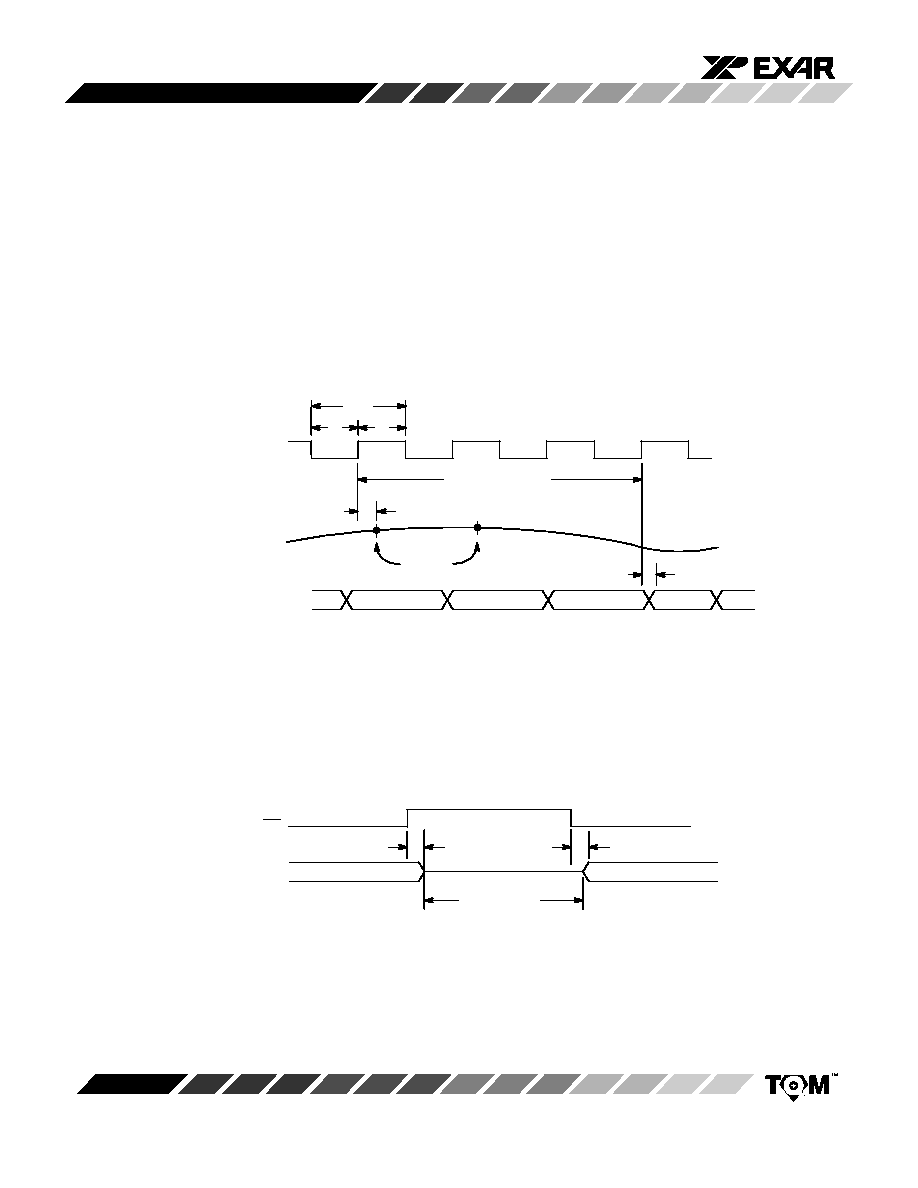
Pipeline Delay
N + 1
N + 2
N ≠ 3
N ≠ 2
N ≠ 1
DATA
(DB0-DB9 and OFW)
High
Impedance
OE
1/FS
t
PWH
Figure 2. XRD6414 Timing Diagram
Figure 3. 3-State Timing Diagram
t
DHZ
t
DEN
t
PWL
N
N+1
N
N+1
t
DL
Sampling
Points
t
AP
Analog
Input
V
IN
N
DATA
(DB0-DB9 and OFW)
XRD6414
7
Rev. 1.00
THEORY OF OPERATION
V
IN
Analog Input
This part has a switched capacitor type input circuit. The
input impedance changes with the phase of the input
clock. V
IN
is sampled at the low to high clock transition
and the digital data changes at the low to high clock
transition. The diagram
Figure 4. shows an equivalent
input circuit.
Figure 4. Equivalent Input Circuit
100
+
-
V
RT
+ V
RB
V
IN
AGND
100
18pF
1.5pF
AV
DD
CLK
C
L
CLK
5pF
2
OFW Overflow (Output)
This signal indicates when the Analog Input (V
IN
) goes
above V
RT
. The pin is normally at a low logic level. When
V
IN
> V
RT
, OFW will go high and the data bits (DB0 ≠ DB9)
will show full scale (i.e. all 1s).
OE Output Enable (Input)
This signal controls the 3-state drivers on the digital
outputs DB0 ≠ DB9 and OFW. During normal operation
OE should be held low so that all outputs are enabled.
When OE is driven high DB0 ≠ DB9 and OFW go into high
impedance mode. This control operates asynchronous to
the clock and will only control the output drivers. The
internal output register will get updated if the clock is
running while the outputs are in three-state mode.
OE
DBO-DB9
OFW
0
Enabled
Enabled
1
Three-Stated
Three-Stated
Table 1. Output Enable
Power Supply Sequencing
There are no power supply sequencing issues if DV
DD
and AV
DD
of the XRD6414 are driven from the same
supply. Best parametric results, however, are obtained
when DV
DD
and AV
DD
are driven from separate supplies.
When DV
DD
and AV
DD
are driven separately, AV
DD
must
come up at the same time or before DV
DD
, and go down at
the same time or after DV
DD
. If the power supply
sequencing in this case is not followed, then damage may
occur to the product due to current flow through the
source-body junction diodes between DV
DD
and AV
DD
. A
low threshold schottky diode placed locally between
DV
DD
and AV
DD
can prevent damage to the XRD6414.
Logic Output Interface
The digital output drive circuitry of the XRD6414 was
designed to operate separately from the analog supplies.
The DV
DD
pin of the XRD6414 is a separate power supply
dedicated to the logic output drivers. DV
DD
is not
connected internally with any of the other power supplies.
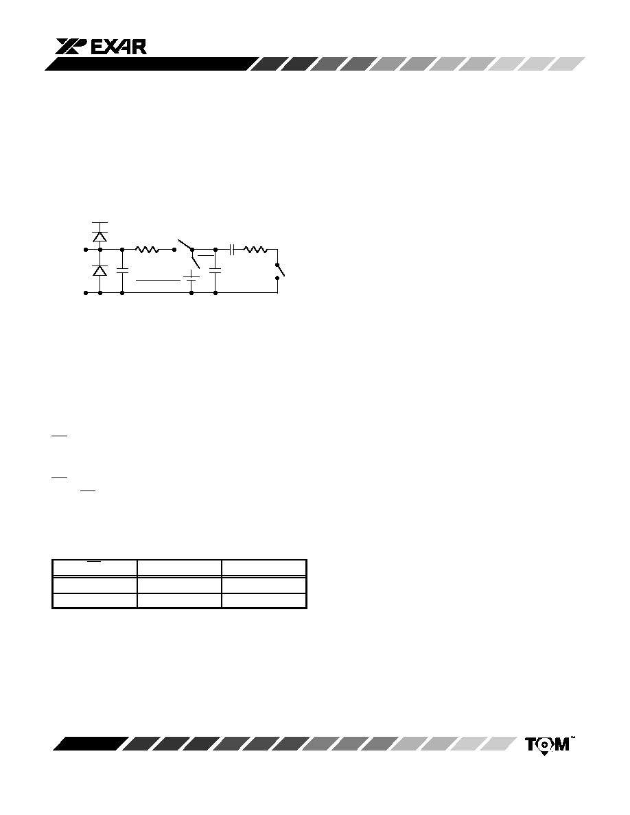
Figure 5. illustrates the power supply circuity of the
XRD6414.
DV
DD
and DGND connect directly to the digital logic
power of the user's system isolating the analog and digital
power supplies and grounds. DGND is not common to the
XRD6414 substrate. The XRD6414 substrate is common
only to the packages' AGND pins. Best spectral
performance is obtained when DV
DD
is lowered to 3.3V.
See the power supply sequencing section if AV
DD
and
DV
DD
are powered separately.

XRD6414
8
Rev. 1.00
FINAL DESIGN CONSIDERATIONS
The XRD6414 can be evaluated with the XRD6414AB
application board. Contact your distributor or sales
person for delivery. Using the XRD6414AB the following
final design considerations can be made.
1.
Be generous with analog and digital ground planes.
Mirror the ground plane with the supply planes. Use
a 5 mil power / ground plane separation if a four layer
board can be used. The XRD6414 substrate is com-
mon to the packages' AGND pins only. DGND and
DV
DD
are separate supplies dedicated to the output
logic drivers of the XRD6414. Connect DGND and
DV
DD
to the power planes of the system's digital log-
ic.
2.
Keep high frequency decoupling capacitors very
close to the A/D pins and minimize the loop area in-
cluded so less flux will induce less noise. Use de-
coupling capacitors in the same locations as on the
XRD6414AB.
3.
Coupling between logic signals and analog circuitry
can easily change a 10-bit system into an 8-bit sys-
tem or worse. Completely separate them. Watch for
coupling opportunities from other sources not im-
mediately associated with the A/D. Don't use switch-
ing power supplies in adjacent locations, for exam-
ple.
4.
The DC performance of the XRD6414 is optimized
with rise and fall times of CLK edges limited to great-
er than or equal to 10ns. A resistor in series with the
CLK input pin can combine with parasitic capaci-
tance to limit rise and fall times. Select a low jitter
clock with a 50% duty cycle for best spectral results.
5.
Use support devices equivalent to those used on the
evaluation board. Use the application board to verify
these devices up front, i.e. use very linear passive
components in the signal path.
6.
Select a driving op amp whose noise, speed, and lin-
earity fits the application. Use a resistor to decouple
the output of the driving op amp from the switching
input capacitance of the XRD6414.
7.
DNL and INL performance is optimized when the
V
RB
input of the XRD6414 is buffered. If V
RB
is con-
nected to the PCB ground plane it is subject to the
noise and ground bounce in that plane. For example
V
RB
could be buffered to 50mV above ground and
still have a wide reference voltage range set by con-
necting V
RT
to a voltage near AV
DD
.
8.
Use 50 or 100
resistors to isolate the XRD6414 dig-
ital output pins from a latch or bus connection. This
protects the output drivers and reduces the effects of
high speed switching logic signals from degrading
the ADC performance. Layout the latch or digital
buffers as close to the ADC as possible to minimize
trace length.
A/D Circuit
AV
DD
DV
DD
DGND
AGND
DB(0-9)
& OFW
Source≠body junction diode
between DV
DD
& AV
DD
Source≠body junction
diode between DGND
& AGND
Figure 5. XRD6414 ADC Power Supply
Circuit Allows Separate AV
DD
& DV
DD
and Separate AGND & DGND
XRD6414
9
Rev. 1.00
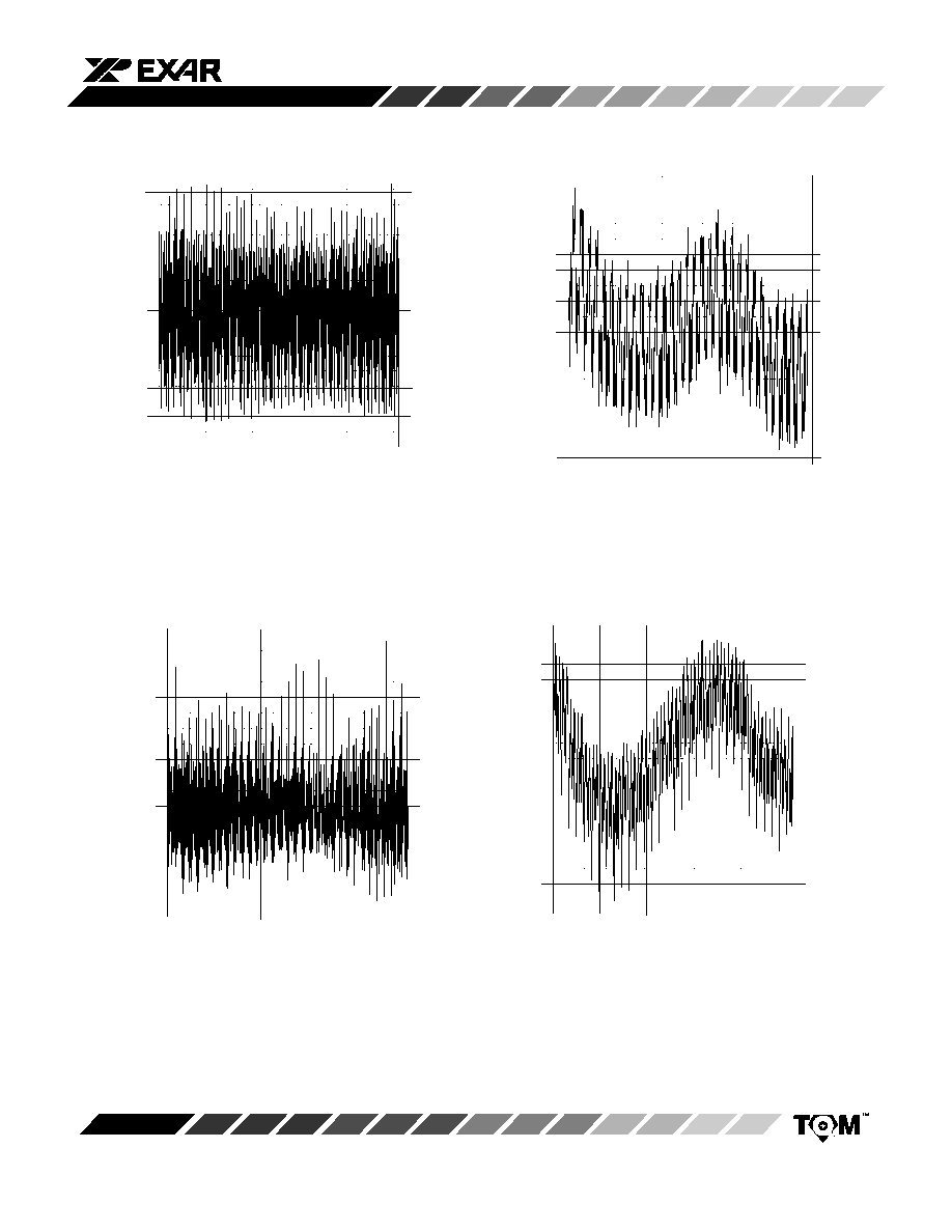
Figure 6. XRD6414, DNL @ 15MSPS
AV
DD
= 5V, V
RT
= 2.5V, V
RB
= 0.5V
Figure 7. XRD6414, INL @ 15MSPS
AV
DD
= 5V, V
RT
= 2.5V, V
RB
= 0.5V
Figure 8. XRD6414, DNL @ 15MSPS
AV
DD
= 5V, V
RT
= 5V, V
RB
= AGND
Figure 9. XRD6414, INL @ 15MSPS
AV
DD
= 5V, V
RT
= 5V, V
RB
= AGND
0.9
0.8
0.7
0.6
0.5
0.4
0.3
0.2
0.1
0.0
≠0.1
≠0.2
≠0.3
≠0.4
≠0.5
≠0.6
≠0.7
≠0.8
≠0.9
LSB
1.6
1.4
1.2
1.0
0.8
0.6
0.4
0.2
≠0.2
≠0.4
≠0.6
≠0.8
≠1.0
≠1.2
≠1.4
≠1.6
≠1.8
≠2.0
0.55
0.50
0.45
0.40
0.35
0.30
0.25
0.20
0.15
0.10
0.05
0.00
≠0.05
≠0.01
≠0.15
≠0.20
≠0.25
≠0.30
≠0.35
LSB
1.0
0.8
0.6
0.4
0.2
≠0.2
≠0.4
≠0.6
≠0.8
≠1.0
≠1.2
≠1.4
≠1.6
≠1.8
≠2.0
≠2.2
≠2.4
LSB
LSB
0
200
400
600
800
1000
0
200
400
600
800
1000
0
200
400
600
800
1000
0
200
400
600
800
1000
0.0
0.0
CODE
CODE
CODE
CODE
XRD6414
10
Rev. 1.00
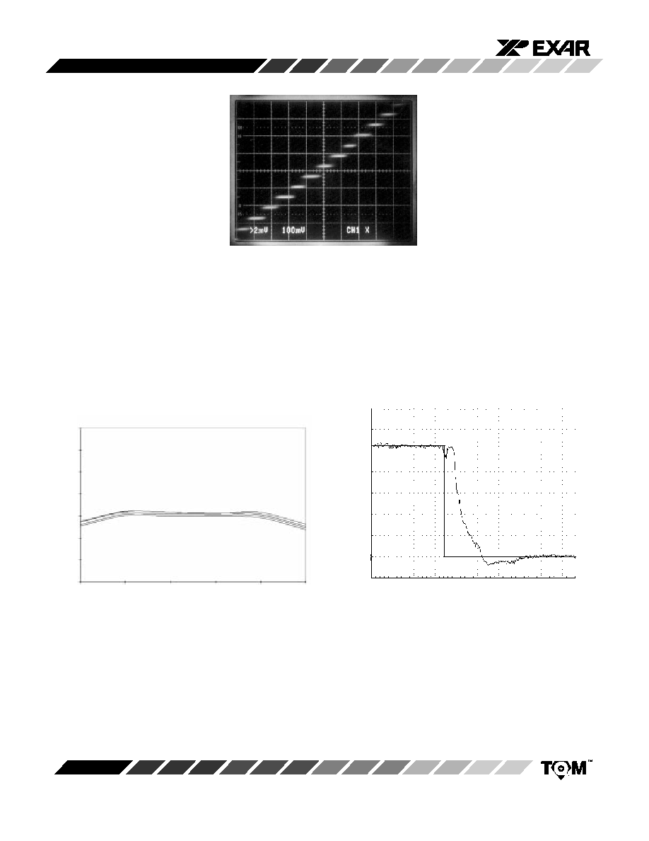
Figure 10. Crossplot Staircase Output
CLK = (15MSPS, t
rf
= 15ns), V
IN
= 3V,
V
REF
= 2V
Figure 11. Analog MUX R
ON
vs. Input Voltage
R
ON
vs. V
IN
R
ON
)
V
IN
(Volts)
(
140
120
100
80
60
40
20
0
0
1
2
3
4
5
AV
DD
= 5V
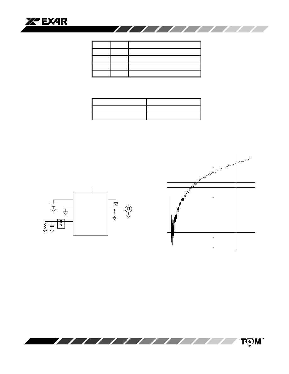
Figure 12. MUX Switching Time Waveform,
AV
DD
= 5V
6.0
5.0
4.0
3.0
2.0
1.0
0.0
≠1.0
t(ns)
0
10
A0
A
OUT
A
OUT
(V)
20
30
40
50
60
70
80
90
XRD6414
11
Rev. 1.00
A1
A0
Selected Analog Input
0
0
A
IN
1
0
1
A
IN
2
1
0
A
IN
3
1
1
A
IN
4
Table 2. Truth Table for Analog Input Selection
PD
Device Status
1
Off (Not Operating)
0
On (Operating)
Table 3. Power Down
Figure 13. MUX Switching Time Test Circuit
V
IN
XRD6414
A
IN1
A
IN2
A
OUT
26pF
10M
W
JP15
(2,3)
AV
DD
(5 V)
50
A1
A0
5V or
3V
AGND
Figure 14. XRD6414 Crosstalk,
AV
DD
= 5V and V
IN
= 8dBm
≠78
≠80
≠82
≠84
≠86
≠88
≠90
≠92
≠94
≠96
≠98
≠100
≠102
≠104
≠106
≠108
≠110
≠112
≠114
0.00
2.00
4.00
6.00
F
IN
(MHz)
Crosstalk (dB)
XRD6414
12
Rev. 1.00
60
59
58
57
56
55
54
53
10
100
1,000
Input Frequency (kHz)
40
30
20
10
0
≠10
≠20
≠30
≠40
≠50
≠60
≠70
≠80
≠90
≠100
≠110
58
10
100
1,000
57
56
55
54
53
52
51
50
49
Input Frequency (kHz)
0.1
0.2
0.3
0.4
0.5
0
A
IN3
XRD6414
A
IN1
V
OUT
50
5V
AV
DD
A
OUT
50
V
IN
VSOURCE
A0
A1
Figure 15. Crosstalk Test Circuit
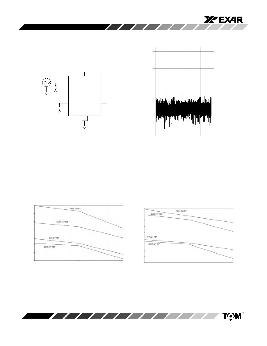
Figure 16. XRD6414 FFT V
REF
= AV
DD
= 5V,
DV
DD
= 3.3V, F
IN
= 100kHz, F
S
=
10MSPS,
C
IN
= 100pF
Figure 17. XRD6414 SNR & SNDR vs. F
IN
,
AV
DD
= 5V, DV
DD
= 3.3V, V
REF
= 5V & 2V,
F
S
= 10MSPS, C
IN
= 100pF
Figure 18. XRD6414 SNR & SNDR vs. F
IN
,
AV
DD
= 5V, DV
DD
= 3.3V, V
REF
= 5V & 2V,
F
S
= 15MSPS, C
IN
= 100pF
AGND
F
IN
/ F
S
dB
dB
dB

XRD6414
13
Rev. 1.00
A
0.055
0.063
1.40
1.60
A
1
0.002
0.006
0.05
0.15
A
2
0.053
0.057
1.35
1.45
B
0.012
0.018
0.30
0.45
C
0.004
0.008
0.09
0.20
D
0.346
0.362
8.80
9.20
D
1
0.272
0.280
6.90
7.10
e
0.0315 BSC
0.80 BSC
L
0.018
0.030
0.45
0.75
0
∞
7
∞
0
∞
7
∞
32 LEAD THIN QUAD FLAT PACK
(7 x 7 x 1.4 mm TQFP)
Rev. 2.00
SYMBOL
MIN
MAX
MIN
MAX
INCHES
MILLIMETERS
24
17
16
9
1
8
25
32
D
D
1
D
D
1
B
e
A
2
A
1
A
Seating Plane
Note: The control dimension is the millimeter column
L
C

XRD6414
14
Rev. 1.00
Notes

XRD6414
15
Rev. 1.00
Notes

XRD6414
16
Rev. 1.00
NOTICE
EXAR Corporation reserves the right to make changes to the products contained in this publication in order to im-
prove design, performance or reliability. EXAR Corporation assumes no responsibility for the use of any circuits de-
scribed herein, conveys no license under any patent or other right, and makes no representation that the circuits are
free of patent infringement. Charts and schedules contained here in are only for illustration purposes and may vary
depending upon a user's specific application. While the information in this publication has been carefully checked;
no responsibility, however, is assumed for inaccuracies.
EXAR Corporation does not recommend the use of any of its products in life support applications where the failure or
malfunction of the product can reasonably be expected to cause failure of the life support system or to significantly
affect its safety or effectiveness. Products are not authorized for use in such applications unless EXAR Corporation
receives, in writing, assurances to its satisfaction that: (a) the risk of injury or damage has been minimized; (b) the
user assumes all such risks; (c) potential liability of EXAR Corporation is adequately protected under the circum-
stances.
Copyright 1996 EXAR Corporation
Datasheet March 1997
Reproduction, in part or whole, without the prior written consent of EXAR Corporation is prohibited.