XRD9810/12
3-Channel 10/12-Bit Linear CCD & CIS
Sensor Signal Processors
Rev. 1.00
E
1999
EXAR Corporation, 48720 Kato Road, Fremont, CA 94538 z (510) 668-7000 z FAX (510) 668-7017
August 1999-1
FEATURES
D
Single 10/12-Bit 8 MSPS A/D Converter
D
Triple-Channel, 2.5 MSPS CCD Color Scan Mode
D
Single-Channel, 6 MSPS Monochrome Scan Mode
CCD or CIS
D
Triple Correlated Double Sampler
D
Triple Programmable Gain Amplifier
D
Serial Programming Interface
D
Differential or Single Ended Inputs
D
CDS for CCD or S/H Mode for CIS Images
D
Inverting or Non-Inverting Mode
D
Internal Voltage Reference
D
5V Operation and 3V I/O Compatibility
D
Low Power CMOS: 500mW @ 5V
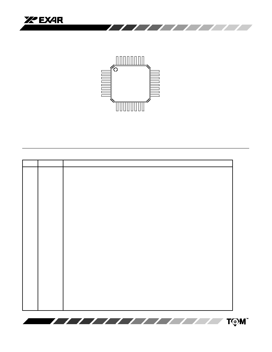
D
32-Pin TQFP Surface Mount Package
APPLICATIONS
D
CCD or CIS Color Scanners
D
Multifunction Products
D
Image Scanners
D
Film Scanners
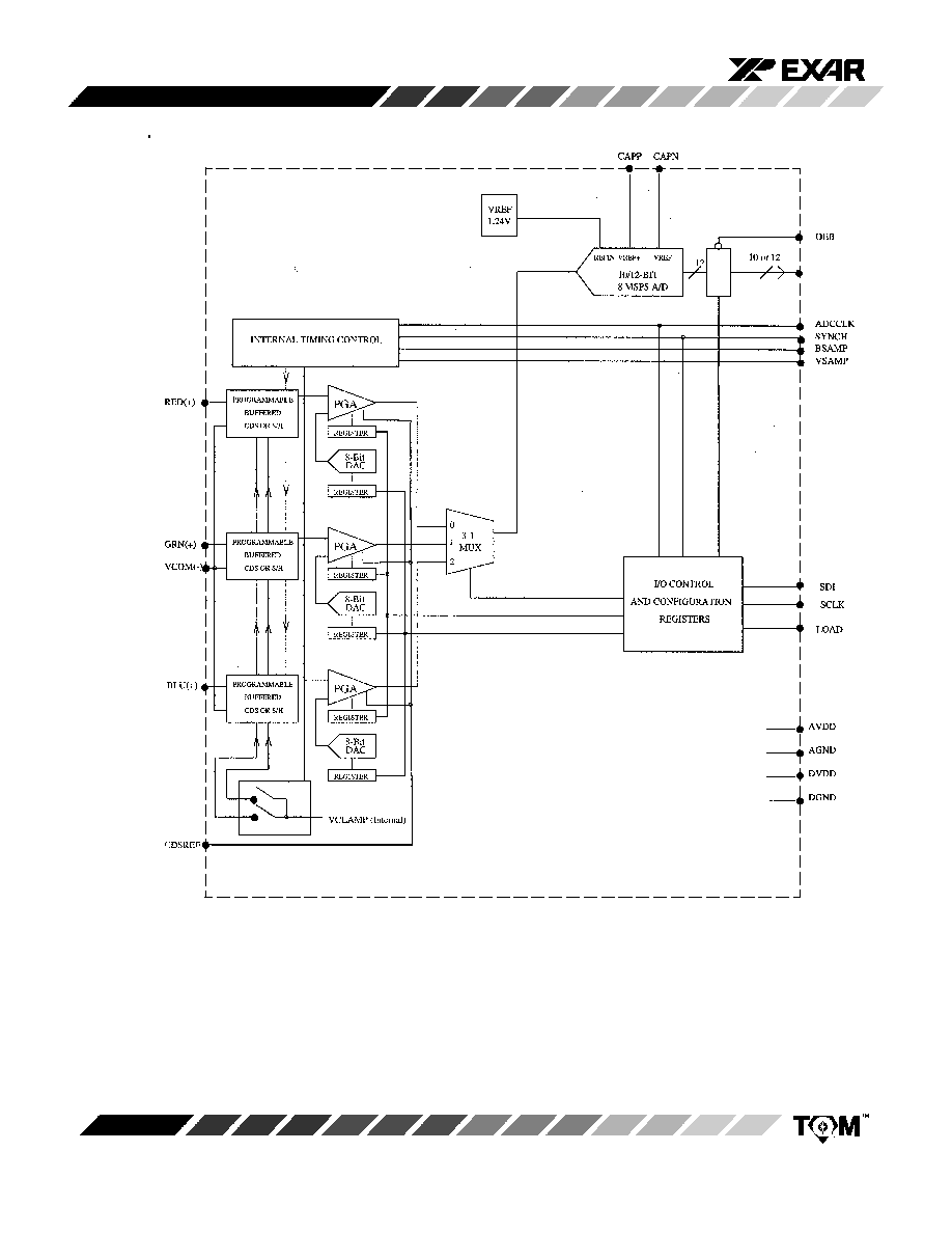
GENERAL DESCRIPTION
The XRD9810/12 is a fully integrated, high-performance
analog signal processor/digitizer specifically designed for
use in 3-channel linear CCD and CIS imaging
applications.
Each channel of the XRD9810/12 includes a Correlated
Double Sampler (CDS), Programmable Gain Amplifier
(PGA) and channel offset adjustment. After gain and
offset adjustment, the analog inputs are sequentially
sampled and digitized by an accurate 10-Bit (XRD9810)
or 12-Bit (XRD9812) A/D converter. The analog front-end
can be configured for inverting/ non-inverting input, CDS
or sample-hold (S/H) mode, or AC/DC coupling, making
the XRD9810/12 ideal for use in CCD, CIS and other data
acquisition applications. The CDS mode of operation
supports both line and pixel-clamp modes and can be
used to achieve significant reduction in system 1/f noise
and CCD reset clock feed-through.
PGA gain and channel offsets can be updated ona line by
line basis. Each channel can have a seperate offset and
gain setting.
The differential inputs reject common mode noise that
can accumulate in a scanner system due to lamp
switching and cabling.
In S/H mode the internal DC-restore voltage clamp can be
enabled or disabled to support AC-coupled or DC inputs.
Sampling mode, PGA gain, channel offset and input
signal polarity are all programmable through a serial
interface. PGA gain (1-10) and channel offset (-300mV to
300mV) are programmable in 256 linear steps. The A/D
Full-Scale Range (FSR) is programmable to 2V or 3V.
ORDERING INFORMATION
Part No.
Package
Operating
Temperature Range
XRD9810ACQ
32-Lead TQFP
0
�
C to +70
�
C
XRD9812ACQ
32-Lead TQFP
0
�
C to +70
�
C
XRD9810/12
3
Rev. 1.00
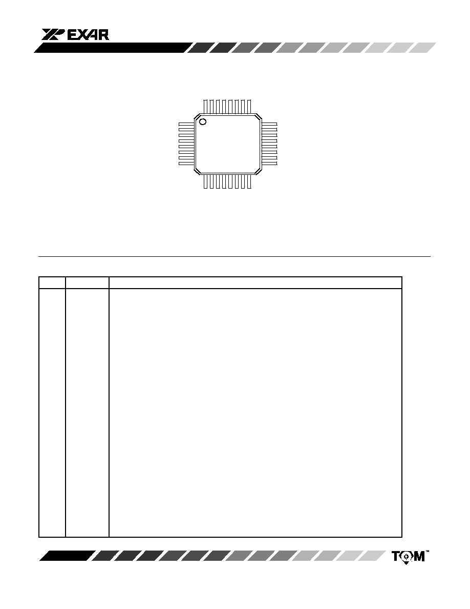
32 Lead TQFP (7 x 7 x 1.4 mm)
D
B
0
N
C
N
C
O
E
B
A
D
C
C
L
K
S
D
I
S
C
L
K
L
O
A
D
DB1
DB2
DB3
DB4
DGND
D
VDD
DB5
DB6
BSAMP
VSAMP
SYNCH
A
VDD2
AGND
CAPN
CAPP
CDSREF
XRD9810ACQ
D
B
7
D
B
8
D
B
9
A
V
D
D
1
R
E
D
(
+
)
V
C
O
M
(
-
-
)
G
R
N
(
+
)
B
L
U
(
+
)
PIN DESCRIPTION
Pin #
Symbol
Description
1
DB1
Data Output Bit 1
2
DB2
Data Output Bit 2
3
DB3
Data Output Bit 3
4
DB4
Data Output Bit 4
5
DGND
Ground (Output Drivers and Internal Decode Logic)
6
DV
DD
Digital Power Supply (Output Drivers and Internal Decode Logic)
7
DB5
Data Output Bit 5
8
DB6
Data Output Bit 6
9
DB7
Data Output Bit 7
10
DB8
Data Output Bit 8
11
DB9
Data Output Bit 9 (MSB)
12
AV
DD1
Analog Power Supply
13
RED(+)
Red Positive Analog Input
14
VCOM(--)
Common Negative Input for positive analog inputs (pins 13,15 and 16)
15
GRN(+)
Green Positive Analog Input
16
BLU(+)
Blue Positive Analog Input
17
CDSREF
Decoupling Cap for CDS Reference
18
CAPP
Decoupling Cap for Positive Reference
19
CAPN
Decoupling Cap for Negative Reference
20
AGND
Analog Ground (Substrate)
21
AV
DD2
Analog Power Supply
XRD9810/12
5
Rev. 1.00
32 Lead TQFP (7 x 7 x 1.4 mm)
D
B
9
D
B
1
0
D
B
1
1
A
V
D
D
1
R
E
D
(
+
)
V
C
O
M
(
-
-
)
G
R
N
(
+
)
B
L
U
(
+
)
BSAMP
VSAMP
SYNCH
AV
DD2
AGND
CAPN
CAPP
CDSREF
XRD9812ACQ
D
B
2
D
B
1
D
B
0
O
E
B
L
O
A
D
S
D
I
S
C
L
K
A
D
C
C
L
K
DB3
DB4
DB5
DB6
DGND
DV
DD
DB7
DB8
PIN DESCRIPTION
Pin #
Symbol
Description
1
DB3
Data Output Bit 3
2
DB4
Data Output Bit 4
3
DB5
Data Output Bit 5
4
DB6
Data Output Bit 6
5
DGND
Ground (Output Drivers and Internal Decode Logic)
6
DV
DD
Digital Power Supply (Output Drivers and Internal Decode Logic)
7
DB7
Data Output Bit 7
8
DB8
Data Output Bit 8
9
DB9
Data Output Bit 9
10
DB10
Data Output Bit 10
11
DB11
Data Output Bit 11 (MSB)
12
AV
DD1
Analog Power Supply
13
RED(+)
Red Positive Analog Input
14
VCOM(--)
Common Negative Input for positive analog inputs (pins 13,15 and 16)
15
GRN(+)
Green Positive Analog Input
16
BLU(+)
Blue Positive Analog Input
17
CDSREF
Decoupling Cap for CDS Reference
18
CAPP
Decoupling Cap for Positive Reference
19
CAPN
Decoupling Cap for Negative Reference
20
AGND
Analog Ground (Substrate)
21
AV
DD2
Analog Power Supply