EXAR Corporation, 48720 Kato Road, Fremont, CA 94538
∑
(510) 668-7000
∑
FAX (510) 668-7017
∑
www.exar.com
Rev. 1.00
XRD9814/XRD9816
3-Channel 14/16-Bit Linear
CCD/CIS Sensor Signal Processors
December 1999-2
FEATURES
∑
14-Bit (XRD9814) or 16-Bit (XRD9816)
A/D Converter
∑
No Missing Codes
∑
Triple-Channel, 2.5 MSPS Color Scan Mode
∑
Single-Channel, 6 MSPS Monochrome Scan
Mode
∑
Triple Correlated Double Sampler
∑
Triple 10-Bit Programmable Gain Amplifier
∑
Triple 10-Bit Offset Compensation DAC
∑
Fully Differential or Single-Ended Inputs
∑
CDS or S/H Mode
∑
Inverting or Non-Inverting Mode
∑
Internal Voltage Reference
∑
Serial Control: On Data Bus or Separate Pins
APPLICATIONS
∑
48-Bit Color Scanners (XRD9816)
∑
42-Bit Color Scanners (XRD9814)
∑
CCD or CIS Color Imagers
∑
Gray Scale Scanners
∑
Film Scanners
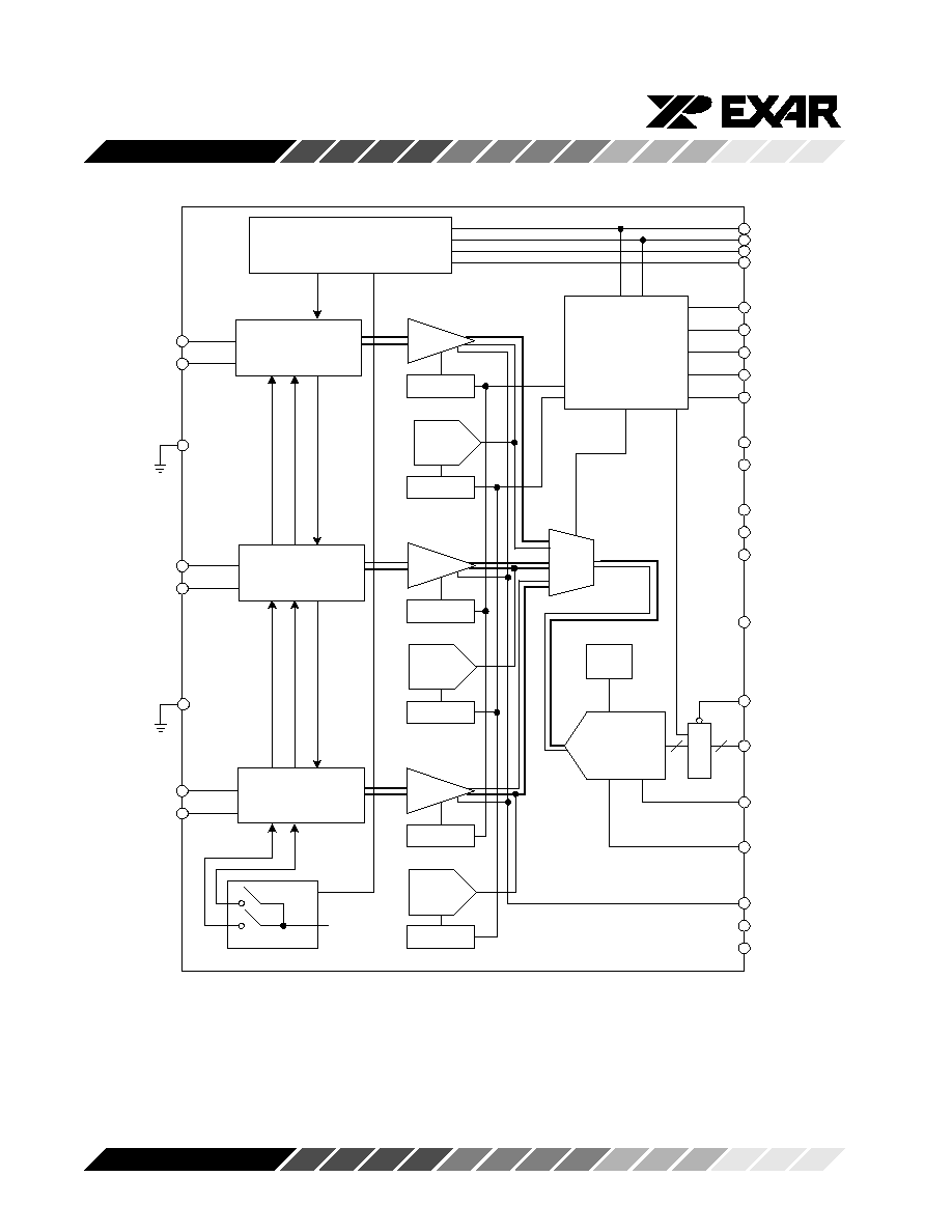
GENERAL DESCRIPTION
The XRD9814/9816 is a fully integrated, high-perfor-
mance analog signal processor/digitizer specifically
designed for use in 3-channel linear Charge Coupled
Device (CCD) and Contact Image Sensitive (CIS)
imaging applications.
Each channel of the XRD9814/9816 includes a Corre-
lated Double Sampler (CDS), Programmable Gain
Amplifier (PGA) and channel offset adjustment. After
gain and offset adjustment, the analog inputs are
sequentially sampled and digitized by an accurate 14/
16-bit A/D converter. The analog front-end can be
configured for inverting/non-inverting input, CDS or
sample-hold (S/H) mode, or AC/DC coupling,
making the XRD9814/9816 suitable for use in CCD,
CIS and other data acquisition applications.
∑
14-Bit or 8-Bit (Nibble) Parallel Data Output
(XRD9814)
∑
16-Bit or 8-Bit (Nibble) Parallel Data Output
(XRD9816)
∑
5V Operation and 3V I/O Compatibility
∑
Low Power CMOS: 500mW @ 5V
The CDS mode of operation supports both line and
pixel-clamp modes and can be used to achieve signifi-
cant reduction in system 1/f noise and CCD reset
clock feed-through. In S/H mode the internal DC-
restore voltage clamp can be enabled or disabled to
support AC-coupled or DC inputs. Sampling mode,
10-bit PGA gain (1024 linear steps), 8-bit fine offset
adjustment (256 linear steps), 2-bit gross offset adjust-
ment and input signal polarity are all programmable
through a serial interface. PGA gain range is 1 to 10,
and channel offset range is -300mV to 300mV for fine
adjustment and additional -400mV to +200mV for
gross offset adjustment. The A/D Full-Scale Range
(FSR) is programmable to 2V or 3V.
ORDERING INFORMATION
Part No.
Package Type
Temperature Range
XRD9814ACV
48-Lead TQFP
0∞C to +70∞C
XRD9816ACV
48-Lead TQFP
0∞C to +70∞C
XRD9814/9816
4
Rev. 1.00
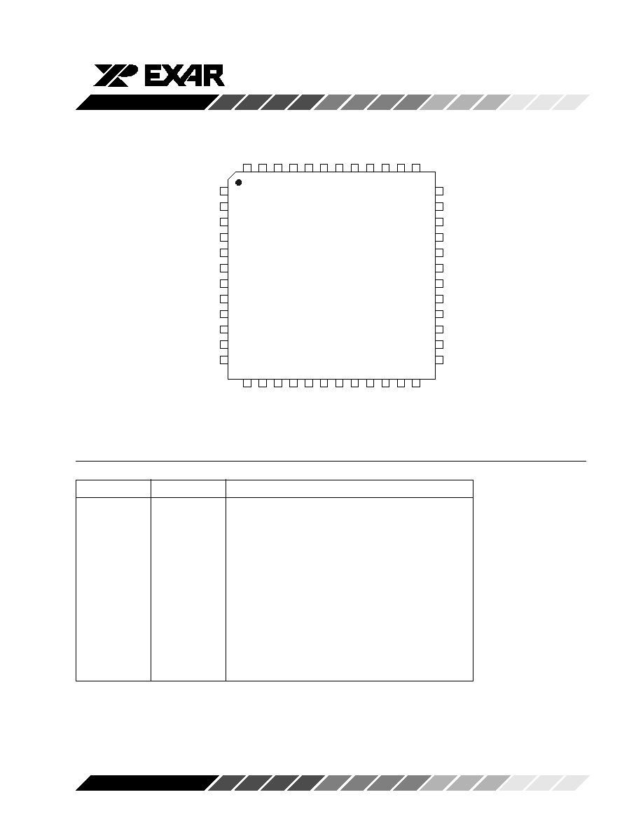
Note 1: INSEL=0 --> SCLK, SDI, and LOAD pins are active for serial programming; INSEL=1 --> SCLK and SDI pins
are inactive, and the serial programming is done through I/O pins DB12 and DB13 as described in Notes 3~4 with
LOAD tri-stating DB12 and DB13.
Note 2: OUTSEL=0 --> 14-bit parallel output mode select; OUTSEL=1 --> 8-bit nibble output mode select.
Note 3: For INSEL=1, DB12 becomes the SCLK input during serial programming.
Note 4: For INSEL=1, DB13 becomes the SDI input during serial programming.
Note 5: Pins 17, 20 and 23 may be connected to AGND2 to improve noise immunity.
PIN DESCRIPTION - XRD9814 (CONT'D)
Pin No.
Name
Description
16
RED(-)
Red Negative Analog Input
17
N/C
No Connect, (Note 5)
18
GRN(+)
Green Positive Analog Input
19
GRN(-)
Green Negative Analog Input
20
N/C
No Connect, (Note 5)
21
BLU(+)
Blue Positive Analog Input
22
BLU(-)
Blue Negative Analog Input
23
N/C
No Connect, (Note 5)
24
TEST1
Internal Use Only
25
TEST2
Internal Use Only
26
CREF
Decoupling Cap for CDS Reference
27
CAPP
Decoupling Cap for Positive Reference
28
CAPN
Decoupling Cap for Negative Reference
29
SGND
Substrate Gnd
30
AGND1
Analog Ground (Substrate)
31
AV
DD1
Analog Power Supply
32
LCLMP
Line Clamp Enable
33
VSAMP
Video Level Sampling Clock
34
BSAMP
Black Level Sampling Clock
35
ADCCLK
A/D Converter Clock
36
INSEL
Input Mode Select (Note 1)
37
OUTSEL
Output Mode Select (Note 2)
38
OEB
Data Output Enable
39
LOAD
Register Write Enable (Note 5)
40
SDI
Serial Data Input (Note 4)
41
SCLK
Serial Shift Clock (Note 3)
42
DGND
Ground (Output Drivers and Internal Decode Logic)
43
DV
DD
Digital Power Supply (Output Drivers and Internal Decode Logic)
44
DB13
Data I/O Bit 13 (Note 4)
45
DB12
Data I/O Bit 12 (Note 3)
46
DB11
Data Output Bit 11
47
DB10
Data Output Bit 10
48
DB9
Data Output Bit 9